AUO 1.2 inch Amoled Datasheet
•
1 like•295 views

Display Type:AMOLED Interface:SPI,MIPI Active Area(mm):30.42(H)×30.42(V) mm Luminance:350 cd/m² (Typ.) Color Depth:16.7M 101% (CIE1931) Learn More For 1.2 Amoled: https://www.panoxdisplay.com/html/products/amoled-31-1.html

Recommended
More Related Content
What's hot
What's hot (20)
Similar to AUO 1.2 inch Amoled Datasheet
Similar to AUO 1.2 inch Amoled Datasheet (20)
More from Panox Display
Recently uploaded
Recently uploaded (20)
AUO 1.2 inch Amoled Datasheet
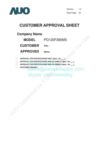
- 1. PO120F390MS Version: 1.2 Total Page: 23 CUSTOMER APPROVAL SHEET Company Name MODEL CUSTOMER APPROVED Title : Name : ˎġ APPROVAL FOR SPECIFICATIONS ONLY (Spec. Ver. ) ˎġ APPROVAL FOR SPECIFICATIONS AND ES SAMPLE (Spec. Ver. ) ˎġ APPROVAL FOR SPECIFICATIONS AND CS SAMPLE (Spec. Ver. ) ˎġ CUSTOMER REMARK : Panox Display sales@panoxdisplay.com skype: panoxwesley
- 2. MODEL NAME: PO120F390MS Version 1.2 Page: 1/23 1 ALL RIGHTS STRICTLY RESERVED. ANY PORTION OF THIS PAPER SHALL NOT BE REPRODUCED, COPIED, OR TRANSFORMED TO ANY OTHER FORMS WITHOUT PERMISSION FROM AU OPTRONICS CORP. Doc. version : 1.2 Total pages : 23 Date : 2017/3/7 Product Specification 1.20" Color AMOLED MP product P/N: < ˓ >Preliminary Specification < >Final Specification Note: The content of this specification is subject to change. © 2016 AU Optronics All Rights Reserved, Do Not Copy. Panox Display sales@panoxdisplay.com skype: panoxwesley
- 3. Version 1.2 Page: 2/23 2 ALL RIGHTS STRICTLY RESERVED. ANY PORTION OF THIS PAPER SHALL NOT BE REPRODUCED, COPIED, OR TRANSFORMED TO ANY OTHER FORMS WITHOUT PERMISSION FROM AU OPTRONICS CORP. Record of Revision Version Revise Date Page Content 0.0 2016-11-1 1~23 First Draft 0.1 2016-11-8 7 Update sleep in mode data 1.0 2016-11-18 4 Update interface information 4 Update pin assignment information 7 Update Display Current Consumption information 11 Update SPI Interface Characteristics 15 Update Power Structure & Power on/off Sequence 17 Update Boost Mode infomation 20 Update ESD criteria 23 Update 2D drawing 1.1 2017-1-17 4 Update outline Dimension 1.2 2017-3-7 23 Update packing information Panox Display sales@panoxdisplay.com skype: panoxwesley
- 4. Version 1.2 Page: 3/23 3 ALL RIGHTS STRICTLY RESERVED. ANY PORTION OF THIS PAPER SHALL NOT BE REPRODUCED, COPIED, OR TRANSFORMED TO ANY OTHER FORMS WITHOUT PERMISSION FROM AU OPTRONICS CORP. Contents A. General Specification ..................................................................................................................................4 1. Physical Specifications ......................................................................................................................4 2. Pin Assignment ...................................................................................................................................4 3. Absolute Maximum Ratings ...............................................................................................................5 B. DC Characteristics.......................................................................................................................................6 1. Typical Operating Conditions ............................................................................................................6 2. Display Current Consumption ...........................................................................................................7 C. AC Characteristics.......................................................................................................................................8 1. MIPI / SPI Interface Characteristics ...................................................................................................8 2. Display RESET Timing Characteristics.......................................................................................... 14 D. Display Coordinate ................................................................................................................................... 16 E. Optical Specification................................................................................................................................. 17 F. Reliability Test Items................................................................................................................................. 20 G. Precautions................................................................................................................................................ 21 H. Packing Information.................................................................................................................................. 22 I. Outline Dimension .................................................................................................................................... 23 Panox Display sales@panoxdisplay.com skype: panoxwesley
- 5. Version 1.2 Page: 4/23 4 ALL RIGHTS STRICTLY RESERVED. ANY PORTION OF THIS PAPER SHALL NOT BE REPRODUCED, COPIED, OR TRANSFORMED TO ANY OTHER FORMS WITHOUT PERMISSION FROM AU OPTRONICS CORP. A. General Specification 1. Physical Specifications NO Item unit Specification Remark 1 Screen Size inch 1.20” 2 Display Resolution -- 390 x 390 3 Outline Dimension mm 33.22 (H) × 34.72 (V) × 0.66(T) 4 Active Area mm 30.42 (H) × 30.42 (V) 5 Color Configuration -- Hyper R.G.B 6 Color Depth -- 16.7M 7 Display Mode -- AMOLED 8 Interface -- MIPI (command mode) + SPI 9 Display IC AUO W022 ASIC 2. Pin Assignment Main FPC Pin assignment — AMOLED Panel Input/Output Signal Interface FPCA recommended connector: BM28B0.6-24DP/2-0.35V(51) Main board recommended connector: BM28B0.6-24DS/2-0.35V(51) Pin location Pin assignment # Pin_name I/O Description 1 ELVSS Power AMOLED negative power supply (Power IC need to follow AUO’s suggestion) 2 ELVDD Power AMOLED positive power supply (Power IC need to follow AUO’s suggestion) 3 ELVSS Power AMOLED negative power supply (Power IC need to follow AUO’s suggestion) 4 ELVDD Power AMOLED positive power supply (Power IC need to follow AUO’s suggestion) Panox Display sales@panoxdisplay.com skype: panoxwesley
- 6. Version 1.2 Page: 5/23 5 ALL RIGHTS STRICTLY RESERVED. ANY PORTION OF THIS PAPER SHALL NOT BE REPRODUCED, COPIED, OR TRANSFORMED TO ANY OTHER FORMS WITHOUT PERMISSION FROM AU OPTRONICS CORP. 5 RESX I Device reset signal (0 : enable ; 1 : Disable) 6 SWIRE O SWIRE signal for PWR IC control 7 NC - Floating 8 GND Power Ground 9 TE I Vsync (vertical sync) signal output from panel to avoid tearing effect 10 DSI_D0N I/O MIPI negative data signal 11 CSX I SPI Enable Signal 12 DSI_D0P I/O MIPI positive data signal 13 SCL I SPI Clock signal 14 GND Power Ground 15 DCX I SPI CMD/Data selection signal 16 DSI_CLKN I MIPI negative clock signal 17 SDI I/O SPI data signal 18 DSI_CLKP I MIPI positive clock signal 19 SDO O SPI Output signal 20 GND Power Ground 21 VCI Power Driver analog power supply (Power IC need to follow AUO’s suggestion) 22 VDDIO Power Power supply for interface system except MIPI interface 23 VCI Power Driver analog power supply 24 VDDIO Power Power supply for interface system except MIPI interface 3. Absolute Maximum Ratings Item Symbol Min. Max. Unit Remark Digital Power Supply VDDIO -0.3 5.5 V Analog Power Supply VCI -0.3 5.5 V ELVDD power Supply ELVDD - 5.0 V ELVSS power Supply ELVSS -5.0 - V Note : If the module exceeds the absolute maximum ratings, it may be damaged permanently. Also, if the module operates with the absolute maximum ratings for a long time, the reliability may drop. Panox Display sales@panoxdisplay.com skype: panoxwesley
- 7. Version 1.2 Page: 6/23 6 ALL RIGHTS STRICTLY RESERVED. ANY PORTION OF THIS PAPER SHALL NOT BE REPRODUCED, COPIED, OR TRANSFORMED TO ANY OTHER FORMS WITHOUT PERMISSION FROM AU OPTRONICS CORP. B. DC Characteristics 1. Typical Operating Conditions Item Symbol Min. Typ. Max. Unit Remark Digital Power Supply VDDIO 1.65 1.8 1.95 V Note1 Analog power Voltage VCI 3.27 3.3 3.33 V Note1 ELVDD power Supply ELVDD 3.27 3.3 3.33 V Note1 ELVSS power Supply ELVSS -3.33 -3.3 -3.27 V Note1 Input Signal Voltage H Level VIH 0.8* VDDIO - VDDIO V Note1 L Level VIL 0 - 0.2* VDDIO V Output Signal Voltage H Level VOH 0.8* VDDIO - VDDIO V Note1 L Level VOL 0 - 0.2* VDDIO V Note1 Note 1: The operation is guaranteed under the recommended operating conditions only. The operation is not guaranteed if a quick voltage change occurs during the operation. To prevent the noise, a bypass capacitor must be inserted into the line closed to the power pin. Panox Display sales@panoxdisplay.com skype: panoxwesley
- 8. Version 1.2 Page: 7/23 7 ALL RIGHTS STRICTLY RESERVED. ANY PORTION OF THIS PAPER SHALL NOT BE REPRODUCED, COPIED, OR TRANSFORMED TO ANY OTHER FORMS WITHOUT PERMISSION FROM AU OPTRONICS CORP. 2. Display Current Consumption Item Symbol Condition Min. Typ. Max. Unit Remark Panel Power POLED ELVDD:3.3V ELVSS:-3.3V -- -- 128.7 mW Note1 IOLED -- -- 19.5 mA Note1 IC Normal PVCI VCI : 3.3V -- 5.3 -- mW Note2 IVCI -- 1.6 -- mA Note2 PVDDIO VDDIO :1.8V -- 3.5 -- mW Note2 IVDDIO -- 1.9 -- mA Note2 Idle PVCI VCI : 3.3V -- 4.5 -- mW Note3/4 IVCI -- 1.4 -- mA Note3/4 PVDDIO VDDIO :1.8V -- 2.4 -- mW Note3/4 IVDDIO -- 1.3 -- mA Note3/4 Sleep PVCI VCI : 3.3V -- 0.075< -- mW IVCI -- 22.6< -- uA PVDDIO VDDIO :1.8V -- 0.1< -- mW IVDDIO -- 55< -- uA Note 1: Based on L255 (350nits) full white pattern Note 2: Based on black pattern / command mode. Note 3: Based on black pattern / MIPI - command mode or SPI interface. Note 4: IVCI < 8mA at Idle mode. Panox Display sales@panoxdisplay.com skype: panoxwesley
- 9. Version 1.2 Page: 8/23 8 ALL RIGHTS STRICTLY RESERVED. ANY PORTION OF THIS PAPER SHALL NOT BE REPRODUCED, COPIED, OR TRANSFORMED TO ANY OTHER FORMS WITHOUT PERMISSION FROM AU OPTRONICS CORP. C. AC Characteristics 1. MIPI / SPI Interface Characteristics MIPI Interface Characteristics HS Data Transmission Burst HS clock transmission Panox Display sales@panoxdisplay.com skype: panoxwesley
- 10. Version 1.2 Page: 9/23 9 ALL RIGHTS STRICTLY RESERVED. ANY PORTION OF THIS PAPER SHALL NOT BE REPRODUCED, COPIED, OR TRANSFORMED TO ANY OTHER FORMS WITHOUT PERMISSION FROM AU OPTRONICS CORP. Turnaround Procedure Bus turnaround (BAT) from MPU to display module timing Timing Parameters Symbol Description Min Typ Max Unit TCLK-POST Time that the transmitter continues to send HS clock after the last associated Data Lane has transitioned to LP Mode. Interval is defined as the period from the end of THS- TRAIL to the beginning of TCLK-TRAIL . 60ns + 52*UI ns TCLK-TRAIL Time that the transmitter drives the HS-0 state after the last payload clock bit of a HS transmission burst. 60 ns THS-EXIT Time that the transmitter drives LP-11 following a HS burst. 300 ns TCLK-TERM-EN Time for the Clock Lane receiver to enable the HS line termination, starting from the time point when Dn crosses VIL,MAX . Time for Dn to reach VTERM- EN 38 ns TCLK-PREPARE Time that the transmitter drives the Clock Lane LP-00 Line state immediately before the HS-0 Line state starting the HS transmission. 38 95 ns TCLK-PRE Time that the HS clock shall be driven by the transmitter prior to any associated Data 8 UI Panox Display sales@panoxdisplay.com skype: panoxwesley
- 11. Version 1.2 Page: 10/23 10 ALL RIGHTS STRICTLY RESERVED. ANY PORTION OF THIS PAPER SHALL NOT BE REPRODUCED, COPIED, OR TRANSFORMED TO ANY OTHER FORMS WITHOUT PERMISSION FROM AU OPTRONICS CORP. Lane beginning the transition from LP to HS mode. TCLK-PREPARE + TCLK-ZERO TCLK-PREPARE + time that the transmitter drives the HS-0 state prior to starting the Clock. 300 ns TD-TERM-EN Time for the Data Lane receiver to enable the HS line termination, starting from the time point when Dn crosses VIL,MAX . Time for Dn to Reach VTERM- EN 35 ns +4*UI THS-PREPARE Time that the transmitter drives the Data Lane LP-00 Line state immediately before the HS-0 Line state starting the HS transmission 40ns + 4*UI 85 ns + 6*UI ns THS-PREPARE + THS-ZERO THS-PREPARE + time that the transmitter drives the HS-0 state prior to transmitting the Sync sequence. 145ns + 10*UI ns THS-TRAIL Time that the transmitter drives the flipped differential state after last payload data bit of a HS transmission burst 60ns + 4*UI ns TLPX(M) Transmitted length of any Low-Power state period of MCU to display module 50 150 ns TTA-SURE(M) Time that the display module waits after the LP-10 state before transmitting the Bridge state (LP-00) during a Link Turnaround. TLPX(M) 2*TLPX(M) ns TLPX(D) Transmitted length of any Low-Power state period of display module to MCU 50 150 ns TTA-GET(D) Time that the display module drives the Bridge state (LP-00) after accepting control during a Link Turnaround. 5*TLPX(D) ns TTA-GO(D) Time that the display module drives the Bridge state (LP-00) before releasing control during a Link Turnaround. 4*TLPX(D) ns TTA-SURE(D) Time that the MPU waits after the LP-10 state before transmitting the Bridge state (LP-00) during a Link Turnaround. TLPX(D) 2*TLPX(D) ns
- 12. Version 1.2 Page: 11/23 11 ALL RIGHTS STRICTLY RESERVED. ANY PORTION OF THIS PAPER SHALL NOT BE REPRODUCED, COPIED, OR TRANSFORMED TO ANY OTHER FORMS WITHOUT PERMISSION FROM AU OPTRONICS CORP. SPI Interface Characteristics Write Cycle in SPI I/F
- 13. Version 1.2 Page: 12/23 12 ALL RIGHTS STRICTLY RESERVED. ANY PORTION OF THIS PAPER SHALL NOT BE REPRODUCED, COPIED, OR TRANSFORMED TO ANY OTHER FORMS WITHOUT PERMISSION FROM AU OPTRONICS CORP. Read Cycle in SPI I/F
- 14. Version 1.2 Page: 13/23 13 ALL RIGHTS STRICTLY RESERVED. ANY PORTION OF THIS PAPER SHALL NOT BE REPRODUCED, COPIED, OR TRANSFORMED TO ANY OTHER FORMS WITHOUT PERMISSION FROM AU OPTRONICS CORP. Serial Interface Characteristics Note: Logic high and low levels are specified as 20% and 80% of VDDIO for Input signals. Note: Ta = -30 to 70 °C, VDDIO=1.65V to 3.3V, VCI=2.7V to 3.6V, GND=0V
- 15. Version 1.2 Page: 14/23 14 ALL RIGHTS STRICTLY RESERVED. ANY PORTION OF THIS PAPER SHALL NOT BE REPRODUCED, COPIED, OR TRANSFORMED TO ANY OTHER FORMS WITHOUT PERMISSION FROM AU OPTRONICS CORP. 2. Display RESET Timing Characteristics Reset input timing Timing Parameters Symbol Parameter Related Pins MIN TYP MAX Note Unit tRESW *1) Reset low pulse width RESX 10 - - - μs tREST *2) Reset complete time - - - 5 When reset applied during Sleep in mode ms - - 120 When reset applied during Sleep out mode ms Note 1. Spike due to an electrostatic discharge on RESX line does not cause irregular system reset according to the table below. RESX Pulse Action Shorter than 5μs Invalid Reset Longer than 10μs Valid Reset Between 5μs and 10μs Reset Initialigation Precedure Note 2. During the resetting period, the display will be blanked (The display is entering blanking sequence, which maximum time is 120 ms, when Reset Starts in Sleep Out –mode. The display remains the blank state in Sleep In –mode) and then return to Default condition for H/W reset. Note 3. During Reset Complete Time, data in OTP will be latched to internal register during this period. This loading is done every time when there is H/W reset complete time (tREST) within 5ms after a rising edge of RESX. Note 4. Spike Rejection also applies during a valid reset pulse as shown below: Note 5. It is necessary to wait 5msec after releasing RESX before sending commands. Also Sleep Out command cannot be sent for 120msec.
- 16. Version 1.2 Page: 15/23 15 ALL RIGHTS STRICTLY RESERVED. ANY PORTION OF THIS PAPER SHALL NOT BE REPRODUCED, COPIED, OR TRANSFORMED TO ANY OTHER FORMS WITHOUT PERMISSION FROM AU OPTRONICS CORP. Operating Sequence Power Structure VBAT PMIC OLED Power IC Host Driver IC Panel Module VDDIO = 1.8V (typ.) VCI = 3.3V (typ.) ELVDD = 3.3V (typ.) ELVSS = -3.3V (typ.) ELVDD ELVSS IOLED SWIRE VCI_EN Display Power on/off Sequence Power on sequence Power off sequence
- 17. Version 1.2 Page: 16/23 16 ALL RIGHTS STRICTLY RESERVED. ANY PORTION OF THIS PAPER SHALL NOT BE REPRODUCED, COPIED, OR TRANSFORMED TO ANY OTHER FORMS WITHOUT PERMISSION FROM AU OPTRONICS CORP. D. Display Coordinate Display scan direction Coordinate Panel Start Point = (0 , 0) Panel End Point = (389 , 389)
- 18. Version 1.2 Page: 17/23 17 ALL RIGHTS STRICTLY RESERVED. ANY PORTION OF THIS PAPER SHALL NOT BE REPRODUCED, COPIED, OR TRANSFORMED TO ANY OTHER FORMS WITHOUT PERMISSION FROM AU OPTRONICS CORP. E. Optical Specification Item Abbr. Min. Typ. Max. Unit Remark Optical Characteristic Brightness 300 350 -- nits Note 3 Contrast ratio @25deg 10000 -- -- Note 4 Brightness Uniformity 350nits 85 -- -- Note 5 Color Temp. T 7500 K Viewing angle CR>1600 Top 80° -- -- deg Note 6 Bottom 80° -- -- deg Left 80° -- -- deg Right 80° -- -- deg Color White CIE1931 x Note 7 White CIE1931 y Red CIE1931 x Red CIE1931 y Green CIE1931 x Green CIE1931 y Blue CIE1931 x Blue CIE1931 y NTSC CIE x , y 87 100 -- % Life time LT95 25°C 150 -- -- hrs Note 8 Flicker -- -- -30 db Note 9 Gamma 2.0 2.2 2.4 Note 10 Boost mode Brightness -- 500 -- Note 11 Note 1: Ambient temperature =25 ºC±2 ºC, measured by CA-310 Note 2: To be measured in the dark room. Note 3: The brightness measurement shall be done at the center of the display with a full white image. Note 4: Definition of contrast ratio: Contrast ratio is calculated with the following formula: Contrast ratio (CR)= Note 5: Uniformity. Refer to figure as below Photo detector output when OLED is at “White” state Photo detector output when OLED is at “Black
- 19. Version 1.2 Page: 18/23 18 ALL RIGHTS STRICTLY RESERVED. ANY PORTION OF THIS PAPER SHALL NOT BE REPRODUCED, COPIED, OR TRANSFORMED TO ANY OTHER FORMS WITHOUT PERMISSION FROM AU OPTRONICS CORP. The test condition at 25ɗ and measured on the surface of display module Measurement equipment: CS2000 or similar equipments ːBp = Bp (Min.) / Bp (Max.)×100 (%) Bp (Max.) = Maximum brightness in 5 measured spots Bp (Min.) = Minimum brightness in 5 measured spots. Note 6: Definition of viewing angle : The optical performance is specified as the driver IC located at =270°ˢ Note 7: The color chromaticity should be based on sample performance because new OLED material should be verified later. Note 8: Time to 95% Luminance To measure the burn-in effect, a test pattern with white background applied to the AMOLED display at 100% loading
- 20. Version 1.2 Page: 19/23 19 ALL RIGHTS STRICTLY RESERVED. ANY PORTION OF THIS PAPER SHALL NOT BE REPRODUCED, COPIED, OR TRANSFORMED TO ANY OTHER FORMS WITHOUT PERMISSION FROM AU OPTRONICS CORP. Note 9: Flicker The flicker level is defined using Fast Fourier Transformation (FTT) as follows: where fFFTC(n) is the nth FFT coefficient, and fFFTC(0) is the 0th FFT coefficient which is DC component. FS(Hz) is the flicker sensitivity as a function of frequency. The flicker level shall be measured with the test pattern in below. The gray leves of test pattern is 128. Note 10 : Gamma spec. is based on Gray level 255, 250, 244, 240, 232, 224, 206, 192, 160, 128, 95, 63, 47 & 31. Note 11 : Boost mode only guarantee the brightness.
- 21. Version 1.2 Page: 20/23 20 ALL RIGHTS STRICTLY RESERVED. ANY PORTION OF THIS PAPER SHALL NOT BE REPRODUCED, COPIED, OR TRANSFORMED TO ANY OTHER FORMS WITHOUT PERMISSION FROM AU OPTRONICS CORP. F. Reliability Test Items Category No. Test items Conditions Remark Reliability (Environment) 1 High Temp. Operation Ta= 70ºC 240 hrs Reliability (Environment) 2 High Temp. Storage Ta= 80 ºC 240 hrs 3 Low Temp. Operation Ta= -20 ºC 240 hrs 4 Low Temp. Storage Ta= -30 ºC 240 hrs 5 High Temp./Humi. Operation Ta= 60 ºC. 90% RH 120 hrs 6 High Temp./Humi. Storage Ta= 60 ºC. 90% RH 240 hrs 7 Thermal Shock -30 ºC ~70 ºC, Dwell for 30 min. 100 cycles Non-operation 8 ⊗ ⊘ ⊗ ⊘ Note 11 9 10 ⊭ ⊛ Judge Criteria: No functional defect. Note 11: ESD position refer to figure as below
- 22. Version 1.2 Page: 21/23 21 ALL RIGHTS STRICTLY RESERVED. ANY PORTION OF THIS PAPER SHALL NOT BE REPRODUCED, COPIED, OR TRANSFORMED TO ANY OTHER FORMS WITHOUT PERMISSION FROM AU OPTRONICS CORP. G. Precautions Please pay attention to the following items when you use the OLED Modules(Panel): 1. Do not twist or bend the module(panel) and prevent the unsuitable external force for display during assembly. 2. Adopt measures for good heat radiation. Be sure to use the module(panel) with in the specified temperature. 3. Avoid dust or oil mist during assembly. 4. Follow the correct power sequence while operating. Do not apply the invalid signal, otherwise, it will cause improper shut down and damage the module(panel). 5. Less EMI: it will be more safety and less noise. 6. Please operate module(panel) in suitable temperature. The response time & brightness will drift by different temperature. 7. Avoid to display the fixed pattern (exclude the white pattern) in a long period, otherwise, it will cause image sticking. 8. Please be sure to turn-off the power when connecting or disconnecting the circuit. 9. Polarizer scratches easily, please handle it carefully. 10. Display surface never likes dirt or stains. 11. A dew drop may lead to destruction. Please wipe off any moisture before using module(panel). 12. Sudden temperature changes cause condensation, and it will cause polarizer damaged. 13. High temperature and humidity may degrade performance. Please do not expose the module(panel) to the direct sunlight and so on. 14. Acetic acid or chlorine compounds are not friends with AMOLED display module(panel). 15. Static electricity will damage the module(panel), please do not touch the module(panel) without any grounded device. 16. Please avoid any static electricity damage (ESD) during producing and operating. 17. Do not disassemble and reassemble the module(panel) by self. 18. Be careful do not touch the rear side directly. 19. No strong vibration or shock. It will cause module(panel) broken. 20. Storage the modules(panel) in suitable environment with regular packing. 21. Be careful of injury from a broken display module(panel). 22. Please avoid the pressure adding to the surface (front or rear side) of modules(panel), because it will cause the display non-uniformity or other function issue.
- 23. Version 1.2 Page: 22/23 22 ALL RIGHTS STRICTLY RESERVED. ANY PORTION OF THIS PAPER SHALL NOT BE REPRODUCED, COPIED, OR TRANSFORMED TO ANY OTHER FORMS WITHOUT PERMISSION FROM AU OPTRONICS CORP. H. Packing Information