

Recommended
Recommended
More Related Content
What's hot
What's hot (20)
Viewers also liked
Viewers also liked (13)
Similar to 10. article azojete vol 11 114 119 dibal
Similar to 10. article azojete vol 11 114 119 dibal (20)
More from Oyeniyi Samuel
More from Oyeniyi Samuel (20)
Recently uploaded
Recently uploaded (20)
10. article azojete vol 11 114 119 dibal
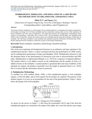
- 1. Arid Zone Journal of Engineering, Technology and Environment. August, 2015; Vol. 11: 114-119 Copyright© Faculty of Engineering, University of Maiduguri, Nigeria. Print ISSN: 1596-2490, Electronic ISSN: 2545-5818 www.azojete.com.ng HYBRID DESIGN, MODELLING, AND SIMULATION OF A 4-BIT BINARY MULTIPLIER USING VIVADO, SIMULINK, AND KINTEX-7 FPGA Dibal, P.Y*. and Ngene, C.U. (Department of Computer Engineering, University of Maiduguri, Maiduguri, Nigeria) Corresponding authors’ email address: yoksa77@gmail.com Abstract The design of binary multipliers is a critical aspect of any reliable hardware in computing and computer engineering. In this paper, the design of a 4 bit binary multiplier has been undertaken, starting with a review of the importance of binary multipliers and wide areas of application. The paper then presents the multiplication methodology which involves an accumulator, a full adder, and a control circuit. The accumulator and full adder were designed using VHDL in the Vivado IDE, whereas the control circuit was modelled using the powerful technique of State flow in Simulink. The 4 bit binary multiplier is then modelled and simulated using the combination of Simulink and VHDL. Results obtained from the simulation verified the accuracy of the design methodology. Keywords: Binary multiplier, simulation, hybrid design, Simulink modeling 1. Introduction One of the most important and fundamental functions in an arithmetic and logic operation is the multiplication function. There is a direct correlation between the performance of a DSP system, and its multiplication performance (Vaidya and Dandekar, 2010). Multiplication function is still the dominant factor in the determination of instruction cycle time in microcontrollers and DSP chips. Multiplication is implemented (Deepali et al., 2013) by a sequence of repeated additions. The number which is to be added is known as the multiplicand, and the number of times it is added is known as the multiplier. A partial product is generated after each step of addition. If the operands are integers, the product is generally twice the length of operands (Sunil et al., 2014); this is to ensure that the information content is protected. 2. Multiplication Methodology To multiply two 4-bit numbers (Roth, 1998), a 4-bit multiplicand register, a 4-bit multiplier register, a 4-bit full adder, and an 8-bit register for the product are required. The purpose of the product register is to serve as an accumulator for the sum of the partial products. Figure 1 below shows the design of the 4-bit multiplier. Figure 1: Design of a 4-bit multiplier As shown by the arrows in Figure 1, 4 bits from the accumulator (ACC) and 4 bits from the multiplicand register are connected to the inputs of the adder; the 4 sum bits and the carry output
- 2. Arid Zone Journal of Engineering, Technology and Environment. August, 2015; Vol. 11: 114-119 115 from the adder are connected back to the accumulator. The adder outputs are transferred to the accumulator when an add signal (Ad) is asserted thus causing the multiplicand to be added to the accumulator. An extra bit at the left end of the product register temporarily stores any carry bits that is generated when the multiplicand is added to the accumulator. When a Shift signal (Sh) occurs, all 9 bits of the ACC are shifted right by the clock pulse. Since the lower 4 bits of the product register are initially unused, we will store the multiplier in this location instead of in a separate register. As each multiplier bits is used, it is shifted out the right end of the register to make room for additional product bits. A shift signal (Sh) causes the contents of the product register to be shifted right one place when the next clock pulse occurs. The control circuit puts out the proper sequence of add and shift signals after a start signal (St = 1) has been received. If the current multiplier bit (M) is 1, the multiplicand is added to the accumulator followed by a right shift; if the multiplier bit is 0, the addition is skipped, and only the right shift occurs. This is demonstrated by the multiplication of (13 x 11) shown in Figure 2 below: 3. Design Methodology From Figure 2, it can be seen that 4 bit binary multiplier circuit is made of three sub-circuits, namely: the control circuit, product block, and the 4 bit adder. The design will be done such that the product block, and the 4 bit full adder will be designed using Vivado IDE (Vivado, 2014), whereas the control circuit will be designed in Simulink. Using the Xilinx Block Set (Simulink, 2014), the entire system will then be integrated to achieve the 4 bit multiplier. Figure 2: Multiplication of 13 x 11
- 3. Dibal and Ngene: Design of a Lock-in Amplifier Micro-Ohmmeter using Proteus VSM. AZOJETE, 11: 114-120 116 3.1 Control Circuit The control shown in Figure 3 is designed such that S0 is the reset state, and the network stays in S0 until a start signal (St = 1) is received. This generates a Load signal which causes the multiplier to be load into the lower 4 bits of the accumulator as shown in Figure 2. In state S1, the low-order bit of the multiplier (M) is tested. If M = 1, an add signal is generated, and if M = 0, a shift is generated. In states S3, S5, and S7, the current multiplier bit (M) is tested to decide whether to generate an add or shift signal. A shift is always generated at the next clock time following an add signal (states S2, S4, S6, and S8). After four shifts have been generated, the control network goes to S9, and a done signal is generated before returning to S0. Figure 3: Control Circuit Design 3.2 Product block and 4 bit Full Adder Design As stated in section 3.0, the design and realization of the product block and the 4 bit full adder will be achieved using the Vivado IDE. Due to space constraint, only a snippet of the code is shown in Figure 4: Figure 4: Code snippet for Product block and 4-bit full adder design
- 4. Arid Zone Journal of Engineering, Technology and Environment. August, 2015; Vol. 11: 114-119 117 3.3 System Integration Using the Xilinx block set family functions, the control circuit design using state flow in Simulink and the Product and 4 bit full adder design in Vivado IDE are integrated and shown in Figure 5: Figure 5: Integration of 4 bit binary multiplier using Xilinx block sets 4. Simulation and Results The design will be simulated using the multiplicand 1101 (which is 13), and the multiplier 1011 (which is 11). These values are inputted into the design as shown in Figure 6. Figure 7: Product of 4 bit binary multiplication operation. Figure 6: Multiplicand and Multiplier Input Upon simulation, the 4 bit multiplier multiplies the multiplicand 1101 by 1011. This gives the binary value of 10001111 which is then converted to the decimal equivalent, as shown in Figure 7.
- 5. Dibal and Ngene: Design of a Lock-in Amplifier Micro-Ohmmeter using Proteus VSM. AZOJETE, 11: 114-120 118 Figure 7: Product of 4 bit binary multiplication operation. Once the multiplication is accomplished, the binary multiplier asserts the Done signal, as shown in Figure 8. Figure 8: Done signal asserted The control signals that make an input to the VHDL entity description for the 4 bit binary multiplier implemented on the Kintex-7 FPGA are shown below in Figure 9. Figure 9: VHDL Control Signals The I/O Planning for the Kintex-7 FPGA is shown below in Figure 10. As can be seen, both the scalar and vector signals have been defined as either input or output, and their locations on the FPGA clearly assigned.
- 6. Arid Zone Journal of Engineering, Technology and Environment. August, 2015; Vol. 11: 114-119 119 Figure 10: Definition and location of scalar and vector signals on Kintex-7 FPGA. Conclusion This paper has been able to design a 4 bit binary multiplier. The design was split into two parts, in which the control circuit was designed using State flow in Simulink and the product block and 4 bit full adder were designed using VHDL in the Vivado IDE. Simulation was conducted and the results obtained as shown in Figure 7, verified the accuracy of the design. References Deepali, C., Gagan, K., Pranay, L., Vidhi, V., and Shailendra, S. 2013. Booth Multiplier: Ease of multiplication. International Journal of Emerging Technology and Advanced Engineering. 3(3): 326 – 330. Roth, CH. 1998. Digital Systems Design Using VHDL. Boston. PWS Publishing Simulink 2014. User Guide. A Publication of MathWorks Inc. Sunil, K., Vishakha, N., Eskinder, A., and Dhok, S. 2014. FPGA Implementation of Single Precision Floating Point Multiplier using High Speed Compressors. International Journal of Soft Computing and Engineering. 4(2): 18 – 23. Vaidya, S., and Dandekar, D. 2010. Delay-Power Performance Comparison of Multipliers in VLSI Circuit Design. International Journal of Computer Networks and Communications. 2(4): 47 – 56. Vivado, 2014. User Guide. A Publication of Xilinx Inc.