
Recommended
More Related Content
What's hot
What's hot (20)
Similar to Digital Clock Using Logic Gates
Similar to Digital Clock Using Logic Gates (20)
More from JalpaMaheshwari1
More from JalpaMaheshwari1 (10)
Recently uploaded
Recently uploaded (20)
Digital Clock Using Logic Gates
- 1. DIGITAL LOGIC DESIGN ME2302-L Final Project Report “DIGITAL CLOCK” CONTENTS Introduction:.........................................................................................................................................3
- 2. Working Logic of the Clock:...............................................................................................................3 Components Required:........................................................................................................................3 Component Description: .....................................................................................................................4 555 Timer IC: .......................................................................................................................................4 Pin Configuration:............................................................................................................................4 4-bit Binary Counter (IC 74LS93): ....................................................................................................4 Pin Configuration:............................................................................................................................4 BCD to Seven Segment Display Decoder (IC74LS47):.....................................................................7 Pin Configuration:............................................................................................................................7 Pin Description:................................................................................................................................7 Seven Segment Display:.......................................................................................................................8 7-Segment Display Format: ................................................................................................................8 Procedure:- ...........................................................................................................................................9 0 to 5 Counter Circuit Diagram: ......................................................................................................10 0 to 9 Counter Circuit Diagram: ......................................................................................................11 Truth Table for 0-9 Counter:............................................................................................................11 Truth Table for 0-5 Counter:............................................................................................................12 Conclusion: .........................................................................................................................................12 References:..........................................................................................................................................12
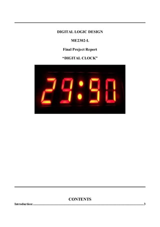
- 3. Introduction: A digital clock is a type of clock that displays the time digitally (i.e. in numerals or other symbols), as opposed to an analog clock, where the time is indicated by the positions of rotating hands. The times derived by analog clocks come from either a pendulum or a spring. Pendulums are unusable on moving platforms, such as a ship, and springs unwind more and more slowly as they release stored up tension. The use of sweep hands allowed these mechanical time bases to be presented in a mechanically driven display. With the perfecting of multivibrator chips, electrical circuits could be built that could accurately keep time under a wide range of conditions. As the time base had switched from mechanical to electrical, the time display had to follow suit. Display devices called 7 segment displays were designed to allow the time to be shown numerically. Working Logic of the Clock: The clock to be designed is something like MM : SS, which represents Minutes and seconds respectively. Now, SS can also be referred as S1 S0 and the same goes for MM. S0 counts from 0 to 9 and then S1 becomes 1 and S0 counts again. Seconds count from 0 - 59. So our S1 counter has to count only from 0-5 and S0 counts 0-9. Thus 0 - 59 will be obtained in the seconds. Now when seconds becomes 60, it is one minute. So every time SS reaches 60, M0 (minutes) should increase by 1. M1 and M0 essentially count the same way as seconds. So, a 1 second pulse given to S0 makes it count from 0 - 9. Whenever S0 reaches 10, a pulse (digital parlance - clock signal) has to be generated to make S0 zero again (digital parlance - reset) and to make S1 one. The process repeats to make S1 two and so on. Thus S1 and S0 will count from 0 - 59. Every time SS reaches 60 a pulse has to be generated to make M0 one and SS 00. For every 60 seconds, SS will go to 59 and back to 0, while MM is incremented. The MM counting is similar to SS but MM receives its clock (triggering pulse) from SS. Components Required: Now, here are the components we need to make the clock: 555 timer IC 7 segment displays 7493 IC 7447 IC Resistors: 10kΩ, 2.2kΩ, 220Ω. Capacitor: 100µF, 10nf. Jumper Wires Cutter Bread Boards 9v Battery
- 4. Vero Board Soldering iron Component Description: 555 Timer IC: Here is a 1Hz pulse/frequency generator using the popular timer IC 555 which is wired as an Astable Multi vibrator. An Astable Multi vibrator, often called a free-running Multi vibrator, is a rectangular- wave generating circuit. This circuit can be used in applications that require clock pulses. An Astable Multi vibrator can be produced by adding resistors and a capacitor to the basic timer IC 555.The timing during which the output is either high or low is determined by the externally connected two resistors and a capacitor. Formula to Calculate 555 timer Frequency: We can set the 555 timer to work at the desired frequency by selecting the right combination of resistances & capacitance. Pin Configuration: 4-bit Binary Counter (IC 74LS93): Pin Configuration:
- 5. Pin Symbol Description 1 CP1 clock input, 2nd, 3rd and 4th section (high-to-low edge-triggered) 2 MR1 asynchronous master reset 3 MR2 asynchronous master reset 4 NC no connection 5 Vcc supply voltage 6 NC no connection 7 NC no connection 8 Q2 counter output 9 Q1 counter output 10 GND ground 11 Q3 counter output 12 Q0 counter output 13 NC no connection 14 CP0 clock input, 1st section (high-to-low edge-triggered) The 7493 datasheet specifies that this counter contains four master-slave flip-flops and additional gating to provide a divide-by-two counter and a three-stage binary counter for which the count cycle length is divide-by-eight for the 7493A. All of these counters have a gated zero reset and the 7490A also has gated set-to-nine inputs for use in BCD nine’s complement applications. IC 7493 is used to make a 4-bit binary counter in the digital clock. If Q0 is connected to input B, we get a 4 bit T flip-flop- Trigger flip flop, (all J & K are internally connected to Vcc) asynchronous counter.
- 6. For a 0 - 9 counter, 1010 (10) should be used as the reset trigger. So Q3and Q1 are connected to R0(1) and R0(2) respectively and we get a 0 - 9 counter. R0(1) and R0(2) are internally connected to a NAND gate which is connected to the CLEAR of all the 4 flip flops. It has the 4 T flip flops and the NAND gate built-in. Input A is given the external clock connection from a 555 astable multi vibrator. Q0 is connected to Input CP1 to complete the asynchronous connection. For a 0 - 5 counter, we use 0110 (6) as the reset trigger. So again Qa is connected to input B to get our 4 bit asynchronous counter. Now Qb and Qc are connected to R0(1) and R0(2) respectively and we get a 0 - 5 counter. In IC 7493, there are only few connections necessary. External clock input from a 555 timer etc, to Input A (Terminal 14). Qa (terminal 12) connected to Input B (terminal 1). Qd, Qc, Qb, Qa of IC 7493 are given as inputs DCBA of the IC 7447 and the rest of the display connections are the same
- 7. with the current limiting resistors. The required resetting connections (which differ for 0-5 counter and 0 -9 counter) have to be made. BCD to Seven Segment Display Decoder (IC74LS47): Pin Configuration: Pin Description: Pin No Function Name 1 BCD Input 2 A1 2 BCD Input 3 A2 3 Display test; Active low LT 4 Ripple blanking output; Active low RBO 5 Ripple blanking input; Active low RBI 6 BCD Input 4 A3 7 BCD Input 1 A0 8 Ground (0V) Ground 9 Segment outputs; Active low e 10 d 11 c 12 b 13 a 14 g 15 f 16 Supply voltage; 5V (4.75V – 5.25V) Vcc The SN54/74LS47are Low Power Schottky BCD to 7-Segment Decoder/Drivers consisting of NAND gates, input buffers and seven AND-OR-INVERT gates. They offer active LOW, high sink current outputs for driving indicators directly. Seven NAND gates and one driver are connected in pairs to make BCD data and its complement available to the seven decoding AND-OR-INVERT gates.
- 8. The remaining NAND gate and three input buffers provide lamp test, blanking input/ripple-blanking output and ripple-blanking input. The circuit accepts 4-bit binary-coded-decimal (BCD) and, depending on the state of the auxiliary inputs, decodes this data to drive a 7-segment display indicator. Output configurations of the SN54/74LS47 are designed to withstand the relatively high voltages required for 7-segment indicators. These outputs will withstand 15 V with a maximum reverse current of 250 µA. Indicator segments requiring up to 24 mA of current may be driven directly from the SN74LS47 high performance output transistors. Display patterns for BCD input counts above nine are unique symbols to authenticate input conditions. The SN54/74LS47 incorporates automatic leading and/or trailing-edge zero-blanking control (RBI and RBO). Lamp test (LT) may be performed at any time which the BI/RBO node is a HIGH level. This device also contains an overriding blanking input (BI) which can be used to control the lamp intensity by varying the frequency and duty cycle of the BI input signal or to inhibit the outputs. Seven Segment Display: Seven-segment displays consist of seven individual colored LED’s (called the segments), within one single display package. In order to produce the required numbers or HEX characters from 0 to 9 and A to F respectively, on the display the correct combination of LED segments need to be illuminated and BCD to 7-segment Display Decoders such as the 74LS47 IC should be used. A standard 7-segment LED display generally has 8 input connections, one for each LED segment and one that acts as a common terminal or connection for all the internal display segments. The Common Cathode Display (CCD) – In the common cathode display, all the cathode connections of the LED’s are joined together to logic “0” or ground. The individual segments are illuminated by application of a “HIGH”, logic “1” signal to the individual Anode terminals. The Common Anode Display (CAD) – In the common anode display, all the anode connections of the LED’s are joined together to logic “1” and the individual segments are illuminated by connecting the individual Cathode terminals to a “LOW”, logic “0” signal. 7-Segment Display Format:
- 9. Procedure:- 1. At first we made the circuit of 555 timer, with the help of 555 timer IC and two resistors of values 10k and 2.2kΩ, and two capacitors of 100µFand 10nF. 2. Then 0-5 counter circuit was made with the help of 555 timer, IC 74LS93 (which is a 4-bit Binary counter IC) and IC 74LS47 (which is a BCD to seven segment display IC). 3. 1 Hz square wave was given as a clock from the 555 timer to the 4-bit binary counter (74LS93). 4. After making the internal connections of the IC 74LS93, we connected the Qa,Qb,Qc and Qd pins of the 7493 IC to give the four bit binary input to the 74LS47( BCD to seven segment decoder). 5. After making the internal connections of IC 74LS47, we connected the, a, b, c, d, e, f and g pins of 7447 to the corresponding pins of the Seven segment display. 6. The SSD used in this clock is Common anode, so its common pin was connected to the Vcc, and the pins were connected to the 7447 IC.
- 10. 0 to 5 Counter Circuit Diagram: 7. Then the 0-9 counter was made in the same manner ( some internal connections of the 7493 IC were different from the 0-5 counter circuit). 8. After making the individual 0-5 and 0-9 counters, the Vcc and ground pins of 0-9 and 0-5 counters were shorted with each other so that the two circuits would get power from the same source, and would work at the same time. 9. The resulting circuit was representing the seconds of digital clock at applying DC power of 9 volts. 10. The whole procedure was repeated for making the circuit for minutes of the digital clock. 11. After making the two individual circuits of 0-5 and 0-9 counters the ground and Vcc lines were shorted with each other. 12. The four individual circuits were connected to each other by three AND gates, to apply trigger so that the 0-9 counter of the seconds will trigger the 0-5 counter of the seconds. When the seconds will reach at 59, it will trigger the minutes to 01, and the cycle will be repeated until 59 minutes, and after then the clock will stop.
- 11. 0 to 9 Counter Circuit Diagram: Truth Table for 0-9 Counter: Inputs Outputs A B C D a b c d e F G 0 0 0 0 1 1 1 1 1 1 0 0 0 0 1 0 1 1 0 0 0 0 0 0 1 0 1 1 0 1 1 0 1 0 0 1 1 1 1 1 1 0 0 1 0 1 0 0 0 1 1 0 0 1 1 0 1 0 1 1 0 1 1 0 1 1 0 1 1 0 0 0 1 1 1 1 1 0 1 1 1 0 1 1 0 0 0 0 1 0 0 0 1 1 1 1 1 1 1 1 0 0 1 1 1 1 0 0 1 1 1 0 1 0 1 1 1 1 1 1 0
- 12. Truth Table for 0-5 Counter: Inputs Outputs A B C D a B c d e F G 0 0 0 0 1 1 1 1 1 1 0 0 0 0 1 0 1 1 0 0 0 0 0 0 1 0 1 1 0 1 1 0 1 0 0 1 1 1 1 1 1 0 0 1 0 1 0 0 0 1 1 0 0 1 1 0 1 0 1 1 0 1 1 0 1 1 0 1 1 0 1 1 1 1 1 1 0 Conclusion: The Digital clock made in this project is a simple Digital clock representing only minutes and seconds, it is a one hour clock and will stop working after one hour. The construction of this clock is very simple. References: http://electel.blogspot.com/2011/12/decoding-ic-74ls47-7-segment-led.html http://home.agh.edu.pl/~ostrowsk/teksty/74ls47.pdf http://www.engineersgarage.com/electronic-components/74ls47-datasheet http://forum.allaboutcircuits.com/threads/how-does-a-74ls47-works-basically.34081/