SlideShare a Scribd company logo
1 of 44
1
CHAPTER 1: INTRODUCTION
1.1 INTRODUCTION
In our minor project, we have shown the concept of AMR (Automatic Meter Reading)
which was purposed for remote monitoring and control of the domestic energy meter by
GSM NET-WORK. This system enables the Electricity Department to read the meter
reading regularly without the person visiting each house. It was achieved by the use of
microcontroller unit that continuously monitored and recorded the Energy Meter
reading in its permanent (non-volatile) memory location. This system also made use of
a GSM model for remote monitoring and control of Energy meter by sending live
reading to electricity department.
Now we have done the further extension of the project by adding the preventive
methods for electricity theft control. The main line theft can be done as shown figure
1.1.
Figure 1.1 Main Line Thefts
2
1.2 MOTIVATION
In India electricity theft leads to annual losses estimated at US$4.5 billion, about 1.5
percent of GDP.
The motivation of this project is to protect electricity from being theft from the various
methods like Tampering with meter seals, by-passing the meters, damaging or
removing meters, illegal tapping to bare wires and illegal taps to low side of the
transformer. The figure below shows the above methods of thefts in figure 1.2.
Figure 1.2 Thefts method
1.3 OBJECTIVE
This project presents detection of power theft in house and in industry for different
methods of theft. Electrical energy is very important for everyday life and is the spine
for the industry. In our daily life with increasing need of electricity the power theft is
also increasing, power theft is a problem that continues to plague power sector across
whole country the objective of this project is to design such a system, which will try to
reduce the illegal use of electricity and reduce the chances of theft. This project will
automatically collect the reading and detect the theft this model reduces manual
manipulation work and try to achieves theft control.
In this project, we use two current transformers to monitor the current status. One
current sensor is connected to the main line and second sensor is connected to the main
3
house after meter. Meter show the reading of home. At the same time main line meter
show the current status of different homes. If anybody hang the wires between pole and
before meter then pole reading is to be exceed automatically and make a big difference
between home reading and pole reading. If the difference is too much then circuit will
automatically send a sms to the control room with theft message.
1.4 CIRCUIT DIAGRAM
Figure 1.3 Circuit diagram of theft monitoring
Figure 1.3 shows the circuit diagram of theft monitoring. It includes energy, meter load, step
down transformer, reset circuitry, 89s52 microcontroller, GSM, LCD, MAX 232 IC, ADC, two
current transformers. ADC converts analog signals to digital signals so that data can be fed to
microcontroller. Microcontroller then analyse the data from both the current transformers and
the data then can be send to authority by GSM.
4
CHAPTER 2: COMPONENTS USED
2.1 Current Transformer (C.T) : The current transformer is a type of "instrument
transformer" that is designed to produce an alternating current in its secondary winding
which is proportional to the current being measured in its primary. Current
transformers reduce high voltage currents to a much lower value and provide a
convenient way of safely monitoring the actual electrical current flowing in an AC
transmission line using a standard ammeter. The principal of operation of a current
transformer is no different from that of an ordinary transformer. The types of current
transformer are shown in fig. 2.1.
Figure 2.1 Typical Current Transformers
Unlike the voltage or Power Transformer looked at previously, the current
transformer consists of only one or very few turns as its primary winding. This primary
winding can be of either a single flat turn, a coil of heavy duty wire wrapped around the
core or just a conductor or bus bar placed through a central hole as shown.
Due to this type of arrangement, the current transformer is often referred too as a
"series transformer" as the primary winding, which never has more than a very few
turns, is in series with the current carrying conductor.
The secondary winding may have a large number of coil turns wound on a laminated
core of low-loss magnetic material which has a large cross-sectional area so that the
magnetic flux density is low using much smaller cross-sectional area wire, depending
5
upon how much the current must be stepped down. This secondary winding is usually
rated at a standard 1 Ampere or 5 Amperes.
The construction of current transformer is shown in figure 2.2.
Figure 2.2 Constructions of current transformers
There are three basic types of current transformers: "wound", "toroidal" and "bar".
• Wound current transformers – The transformers primary winding is physically
connected in series with the conductor that carries the measured current flowing in the
circuit. The magnitude of the secondary current is dependent on the turns ratio of the
transformer.
• Toroidal current transformers – These do not contain a primary winding. Instead, the
line that carries the current flowing in the network is threaded through a window or
hole in the toroidal transformers. Some current transformers have a "split core" which
allows it to be opened, installed, and closed, without disconnecting the circuit to which
they are attached.
• Bar-type current transformers – This type of current transformer uses the actual cable
or bus-bar of the main circuit as the primary winding, which is equivalent to a single
turn. They are fully insulated from the high operating voltage of the system and are
usually bolted to the current carrying device.
Current transformers can reduce or "step-down" current levels from thousands of
amperes down to a standard output of a known ratio to either 5 Amps or 1 Amp for
normal operation. Thus, small and accurate instruments and control devices can be used
with CT's because they are insulated away from any high-voltage power lines. There
are a variety of metering applications and uses for current transformers such as with
6
wattmeter's, power factor meters, watt-hours, protective relays, or as trip coils in
magnetic circuit breakers, So for example, a current transformer with a relationship of
say, 300/5A can be converted to another of 150/5A or even 100/5A by passing the main
primary conductor through its interior window two or three times as shown. This allows
a higher value current transformer to provide the maximum output current for the
ammeter when used on smaller primary current lines.
Current Transformer Primary Turns Ratio
Figure 2.3 Turns ratio in C.T
Example No. 1
A bar-type current transformer which has 1 turn on its primary and 160 turns on its
secondary is to be used with a standard range of ammeters that have an internal
resistance of 0.2Ω's. The ammeter is required to give a full scale deflection when the
primary current is 800 Amps. Calculate the maximum secondary current and secondary
voltage across the ammeter.
Secondary Current:
Voltage across Ammeter:
We can see above that since the secondary of the current transformer is connected
across the ammeter, which has a very small resistance, the voltage drop across the
7
secondary winding is only 1.0 volts at full primary current. If the ammeter is removed,
the secondary winding becomes open-circuited and the transformer acts as a step-up
transformer resulting in a very high voltage equal to the ratio of: Vp(Ns/Np) being
developed across the secondary winding.
So for example, assume our current transformer from above is connected to a 480 volt
three-phase power line. Therefore:
2.2 89S52 MICROCONTROLLER
8051 is the name of a big family of microcontrollers. The device which we used in our
project was the 'AT89S52' which is a typical 8051 microcontroller manufactured by
Atmel™. The block diagram provided by Atmel™ in their datasheet that showed the
architecture of 89S52 device seemed a bit complicated. A simpler architecture can be
represented below.
The 89S52 has 4 different ports, each one having 8 Input/output lines providing a total
of 32 I/O lines. Those ports can be used to output DATA and orders do other devices,
or to read the state of a sensor, or a switch. Most of the ports of the 89S52 have 'dual
function' meaning that they can be used for two different functions.
The first one is to perform input/output operations and the second one is used to
implement special features of the microcontroller like counting external pulses,
interrupting the execution of the program according to external events, performing
serial data transfer or connecting the chip to a computer to update the software. Each
port has 8 pins, and will be treated from the software point of view as an 8-bit variable
called 'register', each bit being connected to a different Input/output pin. The pin
diagram is shown in fig. 2.4.
8
Figure 2.4 Pin Diagram of 8051 Microcontroller
The 8051 MICROCONTROLLER
The 8051 developed and launched in the early 80`s, is one of the most popular micro
controller in use today. It has a reasonably large amount of built in ROM and RAM. In
addition it has the ability to access external memory.
The generic term `8x51` is used to define the device. The value of x defining the kind
of ROM, i.e. x=0, indicates none, x=3, indicates mask ROM, x=7, indicates EPROM
and x=9 indicates EEPROM or Flash.
 About ROM
The early 8051, namely the 8031 was designed without any ROM. This device could
run only with external memory connected to it. Subsequent developments lead to the
development of the PROM or the programmable ROM. This type had the disadvantage
of being highly unreliable.
The next in line, was the EPROM or Erasable Programmable ROM. These devices used
ultraviolet light erasable memory cells. Thus a program could be loaded, tested and
erased using ultra violet rays. A new program could then be loaded again.
9
An improved EPROM was the EEPROM or the electrically erasable PROM. This does
not require ultra violet rays, and memory can be cleared using circuits within the chip
itself.
Finally there is the FLASH, which is an improvement over the EEPROM. While the
terms EEPROM and flash are sometimes used interchangeably, the difference lies in
the fact that flash erases the complete memory at one stroke, and not act on the
individual cells. This results in reducing the time for erasure.
 Architecture
Architecture is must to learn because before learning new machine it is necessary to
learn the capabilities of the machine. This is something like before learning about the
car you cannot become a good driver. The architecture of the 8051 is given below. The
architecture of 8051 microcontroller is shown in fig. 2.4.
 8-bit CPU (Consisting of the ‘A’ and ‘B’ registers)
Most of the transactions within the microcontroller are carried out through the ‘A’
register, also known as the Accumulator. In addition all arithmetic functions are carried
out generally in the ‘A’ register. There is another register known as the ‘B’ register,
which is used exclusively for multiplication and division. Thus an 8-bit notation would
indicate that the maximum value that can be input into these registers is ‘11111111’.
Puzzled?
The value is not decimal 111, 11,111! It represents a binary number, having an
equivalent value of ‘FF’ in Hexadecimal and a value of 255 in decimal.
Figure 2.5 Architecture of 8051 Microcontroller
10
 4K on-chip ROM
Once you have written out the instructions for the microcontroller, where do you put
these instructions.
Obviously you would like these instructions to be safe, and not get deleted or changed
during execution. Hence you would load it into the ‘ROM’.
The size of the program you write is bound to vary depending on the application, and
the number of lines. The 8051 microcontroller gives you space to load up to 4K of
program size into the internal ROM.4K, that’s all? Well just wait. You would be
surprised at the amount of stuff you can load in this 4K of space. Of course you could
always extend the space by connecting to 64K of external ROM if required.
 128 bytes on-chip RAM
This is the space provided for executing the program in terms of moving data, storing
data etc.
 32 I/O lines. (Four- 8 bit ports, labelled P0, P1, P2, P3)
In our bulb example, we used the notation p1.0. This means bit zero of port one. One
bit controls one bulb. Thus, port one would have 8 bits. There are a total of four ports
named p0, p1, p2, p3, giving a total of 32 lines. These lines can be used both as input or
output.
 Two 16 bit timers / counters.
A microcontroller normally executes one instruction at a time. However certain
applications would require that some event has to be tracked independent of the main
program. The manufacturers have provided a solution, by providing two timers. These
timers execute in the background independent of the main program. Once the required
time has been reached, (remember the time calculations described above?), they can
trigger a branch in the main program. These timers can also be used as counters, so that
they can count the number of events, and on reaching the required count, can cause a
branch in the main program.
 Full Duplex serial data receiver / transmitter.
The 8051 microcontroller is capable of communicating with external devices like the
PC etc. Here data is sent in the form of bytes, at predefined speeds, also known as baud
11
rates.
The transmission is serial, in the sense, one bit at a time
 5-Interrupt sources with two priority levels (Two external and three internal):
During the discussion on the timers, we had indicated that the timers can trigger a
branch in the main program. However, what would we do in case we would like the
microcontroller to take the branch, and then return back to the main program, without
having to constantly check whether the required time / count has been reached.
This is where the interrupts come into play. These can be set to either the timers, or
to some external events. Whenever the background program has reached the required
criteria in terms of time or count or an external event, the branch is taken, and on
completion of the branch, the control returns to the main program. Priority levels
indicate which interrupt is more important, and needs to be executed first in case two
interrupts occur at the same time.
 On-chip clock oscillator.
This represents the oscillator circuits within the microcontroller. Thus the hardware is
reduced to just simply connecting an external crystal, to achieve the required pulsing
rate.
SPECIFICATIONS:
 Core Processor: 8051
 Data Bus Width: 8 bit
 Maximum Clock Frequency: 33 MHz
 Program Memory Size: 8 KB
 Program Memory Type: Flash
 RAM Size: 256 B
 ADC: No
 Number of Programmable I/Os: 32
 Number of Timers: 3
 Supply Voltage Range: 4 V to 5.5 V
 Package: PDIP
12
2.3 Liquid crystal display
A liquid crystal display (LCD) is a thin, flat display device made up of any number of
color or monochrome pixels arrayed in front of a light source or reflector. It is prized by
engineers because it uses very small amounts of electric power, and is therefore suitable
for use in battery-powered electronic devices. The LCD is shown in fig. 2.5.
Fig. 2.6 Reflective twisted pneumatic liquid crystal display.
Descriptions of LCD as shown in Fig. 2.5 are as follows:
1. Vertical filter film to polarize the light as it enters.
2. Glass substrate with ITO electrodes. The shapes of these electrodes will
determine the dark shapes that will appear when the LCD is turned on or off. Vertical
ridges etched on the surface are smooth.
3. Twisted pneumatic liquid crystals.
4. Glass substrate with common electrode film (ITO) with horizontal ridges to line
up with the horizontal filter.
5. Horizontal filter film to block/allow through light.
6. Reflective surface to send light back to viewer.
2.3.1 Overview
Each pixel of an LCD consists of a layer of liquid crystal molecules aligned between
two transparent electrodes, and two polarizing filters, the axes of polarity of which are
perpendicular to each other. With no liquid crystal between the polarizing filters, light
passing through one filter would be blocked by the other.
The surfaces of the electrodes that are in contact with the liquid crystal material are
treated so as to align the liquid crystal molecules in a particular direction. This
treatment typically consists of a thin polymer layer that is unidirectional rubbed using a
13
cloth (the direction of the liquid crystal alignment is defined by the direction of
rubbing). The diagram below in figure 2.6 showed a sub pixel of a colour LCD.
Figure 2.7 A sub pixel of a color LCD
Before applying an electric field, the orientation of the liquid crystal molecules is
determined by the alignment at the surfaces. In a twisted pneumatic device (the most
common liquid crystal device), the surface alignment directions at the two electrodes
are perpendicular, and so the molecules arrange themselves in a helical structure, or
twist. Because the liquid crystal material is bi fringe (i.e. light of different polarizations
travels at different speeds through the material), light passing through one polarizing
filter is rotated by the liquid crystal helix as it passes through the liquid crystal layer,
allowing it to pass through the second polarized filter. Half of the light is absorbed by
the first polarizing filter, but otherwise the entire assembly is transparent.
When a voltage is applied across the electrodes, a torque acts to align the liquid crystal
molecules parallel to the electric field, distorting the helical structure (this is resisted by
elastic forces since the molecules are constrained at the surfaces). This reduces the
rotation of the polarization of the incident light, and the device appears gray. If the
applied voltage is large enough, the liquid crystal molecules are completely untwisted
and the polarization of the incident light is not rotated at all as it passes through the
liquid crystal layer. This light will then be polarized perpendicular to the second filter,
and thus be completely blocked and the pixel will appear black. By controlling the
voltage applied across the liquid crystal layer in each pixel, light can be allowed to pass
through in varying amounts, correspondingly illuminating the pixel. With a twisted
pneumatic liquid crystal device it is usual to operate the device between crossed
14
polarizer’s, such that it appears bright with no applied voltage. With this setup, the dark
voltage-on state is uniform. The device can be operated between parallel polarizer’s, in
which case the bright and dark states are reversed (in this configuration, the dark state
appears blotchy).
Both the liquid crystal material and the alignment layer material contain ionic
compounds. If an electric field of one particular polarity is applied for a long period of
time, this ionic material is attracted to the surfaces and degrades the device
performance. This is avoided by applying either an alternating current, or by reversing
the polarity of the electric field as the device is addressed (the response of the liquid
crystal layer is identical, regardless of the polarity of the applied field).
When a large number of pixels is required in a display, it is not feasible to drive each
directly since then each pixel would require independent electrodes. Instead, the display
is multiplexed. In a multiplexed display, electrodes on one side of the display are
grouped and wired together (typically in columns), and each group gets its own voltage
source. On the other side, the electrodes are also grouped (typically in rows), with each
group getting a voltage sink. The groups are designed so each pixel has a unique,
unshared combination of source and sink. The electronics or the software driving the
electronics then turns on sinks in sequence, and drives sources for the pixels of each
sink.
Important factors to consider when evaluating an LCD monitor include resolution,
viewable size, response time (sync rate), matrix type (passive or active), viewing angle,
color support, brightness and contrast ratio, aspect ratio, and input ports (e.g. DVI or
VGA).
2.3.2 Colour display
In colour LCDs each individual pixel is divided into three cells, or sub pixels, which are
colour red, green, and blue, respectively, by additional filters (pigment filters, dye
filters and metal oxide filters). Each sub pixel can be controlled independently to yield
thousands or millions of possible colours for each pixel. Older CRT monitors employ a
similar method.
Colour components may be arrayed in various pixel geometries, depending on the
monitor's usage. If software knows which type of geometry is being used in a given
15
LCD, this can be used to increase the apparent resolution of the monitor through sub
pixel rendering. This technique is especially useful for text anti-aliasing. A general
purpose alphanumeric LCD, with two lines of 16 characters.
LCDs with a small number of segments, such as those used in digital watches and
pocket calculators, have a single electrical contact for each segment. An external
dedicated circuit supplies an electric charge to control each segment. This display
structure is unwieldy for more than a few display elements. Small monochrome
displays such as those found in personal organizers, or older laptop screens have a
passive-matrix structure employing supertwist pneumatic (STN) or double-layer STN
(DSTN) technology (DSTN corrects a colour-shifting problem with STN). Each row or
column of the display has a single electrical circuit. The pixels are addressed one at a
time by row and column addresses. This type of display is called a passive matrix
because the pixel must retain its state between refreshes without the benefit of a steady
electrical charge. As the number of pixels (and, correspondingly, columns and rows)
increases, this type of display becomes less feasible. Very slow response times and poor
contrast are typical of passive-matrix LCDs.
High-resolution color displays such as modern LCD computer monitors and televisions
use an active matrix structure. A matrix of thin-film transistors (TFTs) is added to the
polarizing and color filters. Each pixel has its own dedicated transistor, allowing each
column line to access one pixel. When a row line is activated, all of the column lines
are connected to a row of pixels and the correct voltage is driven onto all of the column
lines. The row line is then deactivated and the next row line is activated. All of the row
lines are activated in sequence during a refresh operation. Active-matrix displays are
much brighter and sharper than passive-matrix displays of the same size, and generally
have quicker response times, producing much better images.
2.3.3 LCD DETAIL
Frequently, an 8051 program must interact with the outside world using input and
output devices that communicate directly with a human being. One of the most
common devices attached to an 8051 is an LCD display. Some of the most common
LCDs connected to the 8051 are 16x2 and 20x2 displays. This means 16 characters per
line by 2 lines and 20 characters per line by 2 lines, respectively.
16
Fortunately, a very popular standard exists which allows us to communicate with the
vast majority of LCDs regardless of their manufacturer. The standard is referred to as
HD44780U, which refers to the controller chip which receives data from an external
source (in this case, the 8051) and communicates directly with the LCD.
44780 BACKGROUNDS
The 44780 standard requires 3 control lines as well as either 4 or 8 I/O lines for the data
bus. The user may select whether the LCD is to operate with a 4-bit data bus or an 8-bit
data bus. If a 4-bit data bus is used, the LCD will require a total of 7 data lines (3
control lines plus the 4 lines for the data bus). If an 8-bit data bus is used, the LCD will
require a total of 11 data lines (3 control lines plus the 8 lines for the data bus).
The three control lines are referred to as EN, RS, and RW.
The EN line is called "Enable." This control line is used to tell the LCD that you are
sending it data. To send data to the LCD, your program should first set this line high (1)
and then set the other two control lines and/or put data on the data bus. When the other
lines are completely ready, bring EN low (0) again. The 1-0 transition tells the 44780 to
take the data currently found on the other control lines and on the data bus and to treat
it as a command.
The RS line is the "Register Select" line. When RS is low (0), the data is to be treated
as a command or special instruction (such as clear screen, position cursor, etc.). When
RS is high (1), the data being sent is text data which should be displayed on the screen.
For example, to display the letter "T" on the screen you would set RS high. The typical
LCD is shown in figure 2.7.
Figure 2.8 A typical LCD
The RW line is the "Read/Write" control line. When RW is low (0), the information on
the data bus is being written to the LCD. When RW is high (1), the program is
17
effectively querying (or reading) the LCD. Only one instruction ("Get LCD status") is a
read command. All others are write commands--so RW will almost always be low.
Finally, the data bus consists of 4 or 8 lines (depending on the mode of operation
selected by the user). In the case of an 8-bit data bus, the lines are referred to as DB0,
DB1, DB2, DB3, DB4, DB5, DB6, and DB7.
2.4 GSM
GSM is a mobile communication modem; it is stands for global system for mobile
communication (GSM). The idea of GSM was developed at Bell Laboratories in 1970.
It is widely used mobile communication system in the world. GSM is an open and
digital cellular technology used for transmitting mobile voice and data services operates
at the 850MHz, 900MHz, 1800MHz and 1900MHz frequency bands.
GSM system was developed as a digital system using time division multiple access
(TDMA) technique for communication purpose. A GSM digitizes and reduces the data,
then sends it down through a channel with two different streams of client data, each in
its own particular time slot. The digital system has an ability to carry 64 kbps to 120
Mbps of data rates. The GSM SIM 900 is shown in figure 2.9.
Figure 2.9 GSM SIM900
2.4.1 GSM Modem
A GSM modem is a device which can be either a mobile phone or a modem device
which can be used to make a computer or any other processor communicate over a
network. A GSM modem requires a SIM card to be operated and operates over a
network range subscribed by the network operator. It can be connected to a computer
through serial, USB or Bluetooth connection.
18
A GSM modem can also be a standard GSM mobile phone with the appropriate cable
and software driver to connect to a serial port or USB port on your computer. GSM
modem is usually preferable to a GSM mobile phone. The GSM modem has wide range
of applications in transaction terminals, supply chain management, security
applications, weather stations and GPRS mode remote data logging.
There are various cell sizes in a GSM system such as macro, micro, pico and umbrella
cells. Each cell varies as per the implementation domain. There are five different cell
sizes in a GSM network macro, micro, pico and umbrella cells. The coverage area of
each cell varies according to the implementation environment.
Time Division Multiple Access
TDMA technique relies on assigning different time slots to each user on the same
frequency. It can easily adapt to data transmission and voice communication and can
carry 64kbps to 120Mbps of data rate.
2.4.2 GSM Architecture
A GSM network consists of the following components:
 A Mobile Station: It is the mobile phone which consists of the transceiver,
the display and the processor and is controlled by a SIM card operating over the
network.
 Base Station Subsystem: It acts as an interface between the mobile station and
the network subsystem. It consists of the Base Transceiver Station which contains the
radio transceivers and handles the protocols for communication with mobiles. It also
consists of the Base Station Controller which controls the Base Transceiver station and
acts as a interface between the mobile station and mobile switching centre.
 Network Subsystem: It provides the basic network connection to the mobile
stations. The basic part of the Network Subsystem is the Mobile Service Switching
Centre which provides access to different networks like ISDN, PSTN etc. It also
consists of the Home Location Register and the Visitor Location Register which
provides the call routing and roaming capabilities of GSM. It also contains the
Equipment Identity Register which maintains an account of all the mobile equipments
19
wherein each mobile is identified by its own IMEI number. IMEI stands for
International Mobile Equipment Identity.
Features of GSM Module:
 Improved spectrum efficiency
 Compatibility with integrated services digital network (ISDN)
 SIM phonebook management
 Fixed dialing number (FDN)
 Real time clock with alarm management
 High-quality speech
 Uses encryption to make phone calls more secure
 Short message service (SMS)
The security strategies standardized for the GSM system make it the most
secure telecommunications standard currently accessible. Although the confidentiality
of a call and secrecy of the GSM subscriber is just ensured on the radio channel, this is
a major step in achieving end-to- end security.
2.5 Step-Down Transformer
Step down transformer from 220 volt Ac to 9-0-9 AC. We use step down transformer to
step down the voltage from 220 to 9 volt ac. This AC is further connected to the
rectifier circuit for AC to DC conversion. Transformer current rating is 750 mA. The
symbol of step down transformer is shown in fig.2.10.
Figure 2.10 Step-down transformer
20
2.6 Reset Circuitry
Pin no 9 of the controller is connected to the reset circuit. On the circuit we connect one
resistor and capacitor circuit to provide a reset option when power is on. As soon as you
give the power supply the 8051 doesn’t start. You need to restart for the microcontroller
to start. Restarting the microcontroller is nothing but giving a Logic 1 to the reset pin at
least for the 2 clock pulses. So it is good to go for a small circuit which can provide the
2 clock pulses as soon as the microcontroller is powered. We are just using a capacitor
to charge the microcontroller and again discharging via resistor. The reset circuitry is
shown in fig. 2.11.
Figure 2.11 Reset Circuitry
2.7 Diode
In this project we use IN 4007 diode as a rectifier. IN 4007 is special diode to convert
the AC into DC In this project we use two diode as a rectifier. Here we use full wave
rectifier. Output of rectifier is pulsating DC. To convert the pulsating dc into smooth dc
we use Electrolytic capacitor as a main filter. Capacitor converts the pulsating dc into
smooth dc and this DC is connected to the Regulator circuit for Regulated 5 volt DC.
The diode and regulated IC is shown in fig. 2.12.
Fig. 2.12 Regulated IC 7805(left side) and diode (right side)
21
Fig. 2.13 Connection of full wave rectifier circuit
Pin no 40 of the controller is connected to the positive supply. Pin no 20 is connected to
the ground. Pin no 9 is connected to external resistor capacitor to provide an automatic
reset option when power is on. In fig.2.13 we can see connection of crystal oscillators.
Figure 2.14 Connection of IC 89s51 to crystal oscillator.
2.8 Crystal Oscillator
Pin no 18 and 19 is connected to external crystal oscillator to provide a clock to the
circuit.
Crystals provide the synchronization of the internal function and to the peripherals.
Whenever ever we are using crystals we need to put the capacitor behind it to make it
free from noises. It is good to go for a 33pf capacitor. The crystal oscillator is shown in
fig. 2.15.
22
Fig. 2.15 Crystal oscillator
We can also resonators instead of costly crystal which are low cost and external
capacitor can be avoided. But the frequency of the resonators varies a lot. And it is
strictly not advised when used for communications projects.
Calculation time required.
The speed with which a microcontroller executes instructions is determined by what is
known as the crystal speed. A crystal is a component connected externally to the
microcontroller. The crystal has different values, and some of the used values are
6MHZ, 10MHZ, and 11.059 MHz etc. Thus a 10MHZ crystal would pulse at the rate of
10,000,000 times per second. The time is calculated using the formula
No of cycles per second = Crystal frequency in HZ / 12.
For a 10MHZ crystal the number of cycles would be,
10,000,000/12=833333.33333 cycles.
This means that in one second, the microcontroller would execute 833333.33333
cycles.
23
CHAPTER 3: INFRARED ALARM FOR METER TAMPERING
3.1 INFRA RED ALARM
Infra red intruder alarm is a very good project to demonstrate the working of the burglar
alarm. In this project when anybody interrupt the light then alarm is automatic on. For
this purpose we use one infra red transmitter L.E.D and one infra red receiver diode as
a receiver component.
All this components is connected to the IC 555. IC 555 is an 8 pin IC. Pin no 4 and 8 is
connected to the positive supply. Pin no 1 is connected to the negative voltage. Pin no 3
is a output pin. Pin no 2 is input trigger pin. Photodiode is connected to the pin no 2.
One buzzer is connected to the pin no 3 via NPN transistor circuit. When light from the
infra red led is focus on the photodiode then photodiode gives a low resistance and so
that pin no 2 is become more positive. When pin no. 2 is become more positive then
output is negative and so that buzzer is off at that time. When anybody interrupts the
light then photodiode is in high resistance and photodiode is off at that time and pin no
2 is become more negative. Now at that time pin no 3 is on high voltage on base of the
transistor and due to this NPN transistor switch on the buzzer circuit
Pin no 6 and 7 of this IC is a time control pin. In this circuit there is no use of timer, so
we connect very small value resistance and one capacitor to pin no 6 and 7.The PIN
diagram of IC 555 is shown here in figure 3.1.
Figure 3.1 IC 555
24
3.2 COMPONENT USED.
3.2.1 IC 555 AND 8 PIN BASE.
 The 555 timer IC is an integral part of electronics projects. Be it a simple
project involving a single 8 bit micro-controller and some peripherals or a complex one
involving system on chips (SoCs), 555 timers working is involved. These provide time
delays, as an oscillator and as a flip-flop element among other applications.
 Introduced in 1971 by the American company Signetics, the 555 is still in
widespread use due to its low price, ease of use and stability. It is made by many
companies in the original bipolar and low-power CMOS types. According to an
estimate, a billion units were manufactured back in the year 2003 alone. (That time,
only 555 i knew was a cough syrup).
 Depending on the manufacturer, the standard 555 package includes 25
transistors, 2 diodes and 15 resistors on a silicon chip installed in an 8-pin mini dual-in-
line package (DIP-8). Variants consist of combining multiple chips on one board.
However 555 are still the most popular.
Some important features of the 555 timer:
555 are used in almost every electronic circuit today. For a 555 timer working as a flip
flop or as a multi-vibrator, it has a particular set of configurations. Some of the major
features of the 555 would be
 It operates from a wide range of power ranging from +5 Volts to +18 Volts
supply voltage.
 Sinking or sourcing 200 mA of load current.
 The external components should be selected properly so that the timing intervals
can be made into several minutes along with the frequencies exceeding several hundred
kilo hertz.
 The output of a 555 timer can drive transistor-transistor logic (TTL) due to its
high current output.
 It has a temperature stability of 50 parts per million (ppm) per degree Celsius
change in temperature which is equivalent to 0.005 % per °C.
25
3.2.2 INFRA RED L.E.D.
An Infrared light emitting diode (IR LED) is a special purpose LED emitting infrared
rays ranging 700 nm to 1 mm wavelength. Different IR LEDs may produce infrared
light of differing wavelengths, just like different LEDs produce light of different colors.
IR LEDs are usually made of gallium arsenide or aluminum gallium arsenide. In
complement with IR receivers, these are commonly used as sensors.
The appearance of IR LED is same as a common LED. Since the human eye cannot see
the infrared radiations, it is not possible for a person to identify if an IR LED is
working. A camera on a cell phone camera solves this problem. The IR rays from the
IR LED in the circuit are shown in the camera.
Figure 3.2 Infrared sensor
3.2.3 CAPACITOR--- 470 mfd, 0.1 mfd and RESISTANCE-1K OHM, 10K OHM,
470 OHM.
3.2.4 PHOTODIODE
A photodiode is a semiconductor device that converts light into an electrical
current. The current is generated when photons are absorbed in the
photodiode. Photodiodes may contain optical filters, built-in lenses, and may have
large or small surface areas.
Figure 3.3 Photo diode symbol
26
3.2.5 NPN TRANSISTOR BC 548
The BC548 is a general-purpose NPN bipolar junction transistor commonly used in
European and American electronic equipment. It is notably often the first type of
bipolar transistor hobbyist’s encounter and is often featured in designs in hobby
electronics magazines where a general-purpose transistor is required.
The BC548 is a part of a family of NPN and PNP epitaxial silicon transistors that
originated with the metal-cased BC108 family of transistors. The BC548 is the modern
plastic-packaged BC108: the BC548 article at the Radio museum website describes the
BC548 as a successor to the BC238 and differing from the BC108 in only the shape of
the package. Datasheets for the BC548 give specifications that are identical to, or
exceed, those of the BC108, BC148 and BC238 predecessors. Thus the BC548 (or
BC546 to 550) is a valid substitute in any circuit designed for the older BC108 (or
BC148), which includes many Mullard and Philips published designs.
3.3 CIRCUIT DIAGRAM
Figure 3.4 INFRARED SENSOR
27
CHAPTER 4: THEFT CONTROL SYSTEM
4.1 INTRODUCTION – Theft Control
In this project we use two current transformers for load measurement. For current
measurement we use CT coil. We use 3200 turns ct coil. This coil is readily available in
the market. In this ct coil there is two wires. These two wires are connected to the
rectifier circuit. We use 4148 diode as a rectifier; we choose 4148 diode for specific
reason. Forward bias voltage drop of the 4148 is approx .3 volts which is less then
silicon diode. Output of the 4148 diode is further connected to the small electrolytic
capacitor for smoothing. Capacitor converts the pulsating dc into smooth dc. Output of
the rectifier is connected to the ADC circuit via variable resistor.
Here we use 0809 ADC for analogue to digital conversion. We choose ADC 0809 for
specific purpose. ADC 0809 has a 8 channel inputs with three address select pins. Pin
no 26, 27 is here use for inputs. Three address pins are 23, 24, 25 which is connected to
pin no 1, 2, 3 of the controller. ADC 0809 provides a parallel output with 8 bit
resolution. Output from the ADC is from pin no 17, 14, 15, 8, 18, 19, 20, and 21. These
8 pins provide a output signal on ADC. This signal is further connected to the port 2
(pin no 21 to 28).
Microcontroller gets the signal and converts into ASCII code. ASCII code is connected
to the LCD display via port 0. We use 2 by 16 LCD. Pin no 2 of the LCD is connected
to the positive 5 volt supply. Pin no 1, 16 of the LCD is connected to ground. Pin no 15
Figure 4.1 LCD connection
28
is connected to the positive 5 volt via series diode. Data from the controller is
connected to the LCD data pin in parallel. Pin no 4, 5, 6 is control pin of the LCD. The
LCD connection is shown below in figure 4.1.
4.2 STEALING
The metering of electric energy meter is mainly according to the relationship with
voltage, electric current and power factor angle. The behaviour of electricity stealing
not only makes the power industry suffering huge financial losses but also threatens the
main power supply security and reliability. According to the analysis, there are many
electricity stealing trick about electric energy meter, the methods could be
approximately divided into under voltage, under current, phase shifted and difference
expansion to their principle. Some common tricks: Un-hooking technology will
electricity stealing. Secretly destroy the lead sealing of electric energy meter, open
voltage hook of terminal in junction box and make no electric current through all using
quantity of electricity steal. One fire-one ground technology. Take the ground. Wire as
naught line, generally take the water pipe or cal duct as ground wire, the risk is bigger
(most dangerous). Violated wire connection. Loop of short electric current, which
makes the electric energy meter shift slow. Cross meter to connect wire, added bypass
to reel across electric energy meter, which makes no or less electric current through,
stall or rear measurement. Exchange fire wire and zero wire. Reverse the in and out of
fire. Make electric meter reverse by using external supply. Adopt hand generator with
voltage and current output or inverter power supply to join into the electric meter, make
the electric energy meter reverse rapidly (rarely used technique and dangerous) As in
fig 7, Due to the kind of electricity stealing and actual demand of preventing electricity
stealing, based on that equipment of electricity stealing with remote monitoring is
designed, which not only monitors the time electricity stealing occur but also offers the
electricity stealing quantity and sends SMS to the local field man to catch the thief with
positive proof to handle lawbreakers with the behaviour of electricity stealing.
4.3 ANALOG TO DIGITAL CONVERTER
From the name itself it is clear that it is a converter which converts the analog
(continuously variable) signal to digital signal. This is really an electronic integrated
circuit which directly converts the continuous form of signal to discrete form. It can be
expressed as A/D or A-to-D or A-D or ADC. The input (analog) to this system can have
29
any value in a range and are directly measured. But for output (digital) of an N-bit A/D
converter, it should have only 2N discrete values. This A/D converter is a linkage
between the analog (linear) world of transducers and discreet world of processing the
signal and handling the data. The digital to analog converter (DAC) carry out the
inverse function of the ADC. The schematic representation of ADC is shown below IN
FIG. 4.2.
Figure 4.2 schematic representation of ADC
ADC Process
There are mainly two steps involves in the process of conversion. They are:-
 Sampling and Holding
 Quantizing and Encoding
The whole ADC conversion process is shown in figure 4.3.
Figure 4.3 ADC conversion process
Sampling and Holding
In the process of Sample and hold (S/H), the continuous signal will gets sampled and
freeze (hold) the value at a steady level for a particular least period of time. It is done to
remove variations in input signal which can alter the conversion process and thereby
30
increases the accuracy. The minimum sampling rate has to be two times the maximum
data frequency of the input signal.
Quantizing and Encoding
For understanding quantizing, we can first go through the term Resolution used in
ADC. It is the smallest variation in analog signal that will result in a variation in the
digital output. This actually represents the quantization error.
V → Reference voltage range 2N → Number of states N → Number of
bits in digital output Quantizing: It is the process in which the reference signal is
partitioned into several discrete quanta and then the input signal is matched with the
correct quantum. Encoding: Here; for each quantum, a unique digital code will be
assigned and after that the input signal is allocated with this digital code. The process of
quantizing and encoding is demonstrated in the table below.
Table 4.1 analog to digital data
From the above table we can observe that only one digital value is used to represent the
whole range of voltage in an interval. Thus, an error will occur and it is called
quantization error. This is the noise introduced by the process of quantization. Here the
maximum quantization error is
Improvement of Accuracy in ADC
Two important methods are used for improving the accuracy in ADC. They are by
increasing the resolution and by increasing the sampling rate. This is shown in figure
below fig. 4.4.
31
Figure 4.4 sampling
Types of Analog to Digital Converter
 Successive Approximation ADC: This converter compares the input signal with the
output of an internal DAC at each successive step. It is the most expensive type.
 Dual Slope ADC: It have high accuracy but very slow in operation.
 Pipeline ADC: It is same as that of two step Flash ADC.
 Delta-Sigma ADC: It has high resolution but slow due to over sampling.
 Flash ADC: It is the fastest ADC but very expensive.
 Other: Staircase ramp, Voltage-to-Frequency, Switched capacitor, tracking, Charge
balancing, and resolver.
Application of ADC
 Used together with the transducer.
 Used in computer to convert the analog signal to digital signal.
 Used in cell phones.
 Used in microcontrollers.
 Used in digital signal processing.
 Used in digital storage oscilloscopes.
 Used in scientific instruments.
 Used in music reproduction technology etc.
32
4.3.1 Circuit diagram
Figure 4.5 ADC pin diagram
4.4 MAX 232
The MAX232 is an integrated circuit first created in 1987 by Maxim Integrated
Products that converts signals from a TIA-232 (RS-232) serial port to signals suitable
for use in TTL-compatible digital logic circuits. The MAX232 is a dual transmitter /
dual receiver that typically is used to convert the RX, TX, CTS, RTS signals.
The drivers provide TIA-232 voltage level outputs (about ±7.5 volts) from a single 5-
volt supply by on-chip charge pumps and external capacitors. This makes it useful for
implementing TIA-232 in devices that otherwise do not need any other voltages.
The receivers reduce TIA-232 inputs, which may be as high as ±25 volts, to standard 5
volt TTL levels. These receivers have a typical threshold of 1.3 volts and a
typical hysteresis of 0.5 volts.
The MAX232 replaced an older pair of chips MC1488 and MC1489 that performed
similar RS-232 translation. The MC1488 quad transmitter chip required 12 volt and -12
volt power,[1] and MC1489 quad receiver chip required 5 volt power.[2] The main
disadvantages of this older solution was the +/- 12 volt power requirement, only
supported 5 volt digital logic, and two chips instead of one.
Controller output is connected to the GSM modem serially via MAS232 IC. We use
max232 IC is convert TTL data to RS232. Here we use sim300/sim900 GSM modem at
the baud rate of 9600.
33
Figure 4.6 RS MAX 232
4.4.1 VOLTAGE LEVELS
The MAX232 translates a TTL logic 0 input to between +3 and +15 V, and
changes TTL logic 1 input to between −3 and −15 V, and vice versa for
converting from TIA-232 to TTL.
Table 4.2: Voltage Level Description of MAX RS 232
TIA-232 line type and
logic level
TIA-232
voltage
TTL voltage
to/from
MAX232
Data transmission (Rx/Tx)
logic 0
+3 V to
+15 V
0 V
Data transmission (Rx/Tx)
logic 1
−3 V to
−15 V
5 V
Control signals
(RTS/CTS/DTR/DSR)
logic 0
−3 V to
−15 V
5 V
Control signals
(RTS/CTS/DTR/DSR)
logic 1
+3 V to
+15 V
0 V
34
4.4.2 Applications
The MAX232 (A) has two receivers that convert from RS-232 to TTL voltage levels,
and two drivers that convert from TTL logic to RS-232 voltage levels. As a result, only
two out of all RS-232 signals can be converted in each direction. Typically, the first
driver/receiver pair of the MAX232 is used for TX and RX signals, and the second one
for CTS and RTS signals.
There are not enough drivers/receivers in the MAX232 to also connect the DTR, DSR,
and DCD signals. Usually, these signals can be omitted when, for example,
communicating with a PC's serial interface, or when special cables render them
unnecessary. If the DTE requires these signals, a second MAX232 or some other IC
from the MAX232 family can be used.
Figure 4.7 max RS 232
35
CHAPTER 5: RESULT AND DISCUSSION
Advanced metering systems can provide benefits for utilities, retail providers and customers.
Benefits will be recognized by the utilities with increased efficiencies, outage detection, tamper
notification and reduced labour cost as a result of automating reads, connections and
disconnects. Retail providers will be able to offer new innovative products in addition to
customizing packages for their customers. In addition, with the meter data being readily
available, more flexible billing cycles would be available to their customers instead of
following the standard utility read cycles. With timely usage information available to the
customer, benefits will be seen through opportunities to manage their energy consumption and
change from one REP to another with actual meter data. Because of these benefits, many
utilities are moving towards implementing some types of AMR solutions.
The government saves money by the control of theft in energy meter and also more beneficial
for customer side and the government side. The metering IC ensures the accurate and reliable
measurement of power consumed. Cost wise low when compared to other energy meter
without automatic meter reading and theft control.
The benefits of smart metering for the utility
 Accurate meter reading, no more estimates
 Improved billing
 Accurate profile classes and measurement classes, true costs applied
 Improved security and tamper detection for equipment.
Disadvantages of automatic meter reading
 Utility can possibly control amount allocated to users.
 Risk of loss of privacy - details of use reveal information about user activities.
 Greater potential for monitoring by other/unauthorized third parties.
36
CHAPTER 6: CONCLUSION
We have studied RF based automatic meter used in different places. We got that this
technology is very useful in present and future demand. AMR served well for commercial and
industrial accounts. The AMR enable us to save million of dollar every year in meter reading
cost and also provide our customer with better information about electricity, more accurate
billing and keep rates as low as we can. The project model reduces the manual manipulation
work and electricity theft .Use of GSM in our system provides the numerous advantages of
wireless network systems. The government can save money by the control of theft in energy
meter and more beneficial for customer side and the government side. The metering IC ensures
the accurate and reliable measurement of power consumed. What was once needed for monthly
data became a need for daily and even hourly reading of the meter. AMR as a way of
improving customer service while reducing the cost of reading meter. Cost wise low when
compared to other energy meter without automatic meter reading and theft control.
The development of GSM based energy meter demonstrates the concept and implementation of
new power metering system. GSM based AMR have low infrastructure cost, low operating
costs, more data security and less man power required. It not only solve the problem of manual
meter reading but also provide additional feature such as power disconnect, power connect ,
power cut alert and tempering alert customer can also pay bill via online login on authenticated
web. Data base server can stored the current month data and also all previous month data for
future use. So it saves a lot amount of time and energy.
37
REFERENCES
[1] Netlab.cs.iitm.ernet.in/cs648/2009/tpf/cs09s022.pdf.
[2] (Online resources-basic electronics), https://electronicsforu.com/resources/learn-
electronics/ , electronics for you (monthly magazine).
[3] Smart and Intelligent GSM based Automatic MeterReading System, International
Journal of Engineering Research & Technology (IJERT),Vol. 1 Issue 3, ISSN: 2278-
0181, May – 2012.
[4] International Journal of Computer Applications (0975 – 8887) Volume 116 – No. 18,
April 2015.
[5] Bharat Kulkarni,”GSM Based Automatic Meter Reading System Using ARM
Controller”,International Journal of Emerging Technology and Advanced Engineering,
ISSN 2250-2459, Volume 2, Issue 5, pp.446-448,May 2012.
[6] PLC (Power Line Communication) Introduction,
www.eetimes.com/document.asp?doc_id=1279014
[7] http://www.itnews.com.au/News/160398,auditor-general-slams-victorian-smart-
meters.aspx
[8] https://en.wikipedia.org/wiki/Automatic_meter_reading#See_also
[9] Amin S. Mehmood, T. Choudhry, M.A. Hanif, “A Reviewing the Technical Issues for
the Effective Construction of Automatic Meter Reading System” in International
Conference on Microelectronics, 2005 IEEE
38
APPENDIX
AN EXAMPLE HARDWARE CONFIGURATION
As we've mentioned, the LCD requires either 8 or 11 I/O lines to communicate with. For the
sake of this tutorial, we are going to use an 8-bit data bus--so we'll be using 11 of the 8051's
I/O pins to interface with the LCD.
Figure 1 LCD connection
As you can see, we've established a 1-to-1 relation between a pin on the 8051 and a line on the
44780 LCD. Thus as we write our assembly program to access the LCD, we are going to
equate constants to the 8051 ports so that we can refer to the lines by their 44780 name as
opposed to P0.1, P0.2, etc. Let's go ahead and write our initial equates:
DB0 EQU P1.0
DB1 EQU P1.1
DB2 EQU P1.2
DB3 EQU P1.3
DB4 EQU P1.4
DB5 EQU P1.5
DB6 EQU P1.6
DB7 EQU P1.7
EN EQU P3.7
RS EQU P3.6
39
RW EQU P3.5
DATA EQU P1
Having established the above equates, we may now refer to our I/O lines by their 44780 name.
For example, to set the RW line high (1), we can execute the following insutrction:
SETB RW
HANDLING THE EN CONTROL LINE
As we mentioned above, the EN line is used to tell the LCD that you are ready for it to execute
an instruction that you've prepared on the data bus and on the other control lines. Note that the
EN line must be raised/lowered before/after each instruction sent to the LCD regardless of
whether that instruction is read or write, text or instruction. In short, you must always
manipulate EN when communicating with the LCD. EN is the LCD's way of knowing that you
are talking to it. If you don't raise/lower EN, the LCD doesn't know you're talking to it on the
other lines.
Thus, before we interact in any way with the LCD we will always bring the EN line high with
the following instruction:
SETB EN
And once we've finished setting up our instruction with the other control lines and data bus
lines, we'll always bring this line back low:
CLR EN
CHECKING THE BUSY STATUS OF THE LCD
As previously mentioned, it takes a certain amount of time for each instruction to be executed
by the LCD. The delay varies depending on the frequency of the crystal attached to the
oscillator input of the 44780 as well as the instruction which is being executed.
While it is possible to write code that waits for a specific amount of time to allow the LCD to
execute instructions, this method of "waiting" is not very flexible. If the crystal frequency is
changed, the software will need to be modified. Additionally, if the LCD itself is changed for
another LCD which, although 44780 compatible, requires more time to perform its operations,
the program will not work until it is properly modified.
40
A more robust method of programming is to use the "Get LCD Status" command to determine
whether the LCD is still busy executing the last instruction received.
The "Get LCD Status" command will return to us two tidbits of information; the information
that is useful to us right now is found in DB7. In summary, when we issue the "Get LCD
Status" command the LCD will immediately raise DB7 if it's still busy executing a command
or lower DB7 to indicate that the LCD is no longer occupied. Thus our program can query the
LCD until DB7 goes low, indicating the LCD is no longer busy. At that point we are free to
continue and send the next command.
Since we will use this code every time we send an instruction to the LCD, it is useful to make it
a subroutine. Let's write the code:
WAIT_LCD:
SETB EN :- Start LCD command
CLR RS :- It's a command
SETB RW :- It's a read command
MOV DATA,#0FFh :-Set all pins to FF initially
MOV A,DATA :- Read the return value
JB ACC.7,WAIT_LCD :- If bit 7 high, LCD still busy
CLR EN :- Finish the command
CLR RW :- Turn off RW for future commands
RET
Thus, our standard practice will be to send an instruction to the LCD and then call our
WAIT_LCD routine to wait until the instruction is completely executed by the LCD. This will
assure that our program gives the LCD the time it needs to execute instructions and also makes
our program compatible with any LCD, regardless of how fast or slow it is.
INITIALIZING THE LCD
Before you may really use the LCD, you must initialize and configure it. This is accomplished
by sending a number of initialization instructions to the LCD.
The first instruction we send must tell the LCD whether we'll be communicating with it with an
8-bit or 4-bit data bus. We also select a 5x8 dot character font. These two options are selected
by sending the command 38h to the LCD as a command. As you will recall from the last
41
section, we mentioned that the RS line must be low if we are sending a command to the LCD.
Thus, to send this 38h command to the LCD we must execute the following 8051 instructions:
SETB EN
CLR RS
MOV DATA,#38h
CLR EN
LCALL WAIT_LCD
We've now sent the first byte of the initialization sequence. The second byte of the
initialization sequence is the instruction 0Eh. Thus we must repeat the initialization code from
above, but now with the instruction. Thus the next code segment is:
SETB EN
CLR RS
MOV DATA,#0Eh
CLR EN
LCALL WAIT_LCD
The last byte we need to send is used to configure additional operational parameters of the
LCD. We must send the value 06h.
SETB EN
CLR RS
MOV DATA,#06h
CLR EN
LCALL WAIT_LCD
INIT_LCD:
SETB EN
CLR RS
MOV DATA,#38h
CLR EN
LCALL WAIT_LCD
SETB EN
CLR RS
MOV DATA,#0Eh
42
CLR EN
LCALL WAIT_LCD
SETB EN
CLR RS
MOV DATA,#06h
CLR EN
LCALL WAIT_LCD
RET
Having executed this code the LCD will be fully initialized and ready for us to send display
data to it.
CLEARING THE DISPLAY
When the LCD is first initialized, the screen should automatically be cleared by the 44780
controller. However, it's always a good idea to do things yourself so that you can be completely
sure that the display is the way you want it. Thus, it's not a bad idea to clear the screen as the
very first opreation after the LCD has been initialized.
An LCD command exists to accomplish this function. Not suprisingly, it is the command 01h.
Since clearing the screen is a function we very likely will wish to call more than once, it's a
good idea to make it a subroutine:
CLEAR_LCD:
SETB EN
CLR RS
MOV DATA,#01h
CLR EN
LCALL WAIT_LCD
RET
How that we've written a "Clear Screen" routine, we may clear the LCD at any time by simply
executing an LCALL CLEAR_LCD.
WRITING TEXT TO THE LCD
Once again, writing text to the LCD is something we'll almost certainly want to do over and
over--so let's make it a subroutine.
43
WRITE_TEXT:
SETB EN
SETB RS
MOV DATA,A
CLR EN
LCALL WAIT_LCD
RET
The WRITE_TEXT routine that we just wrote will send the character in the accumulator to
the LCD which will, in turn, display it. Thus to display text on the LCD all we need to do is
load the accumulator with the byte to display and make a call to this routine. Pretty easy, huh?
A "HELLO WORLD" PROGRAM
Now that we have all the component subroutines written, writing the classic "Hello World"
program--which displays the text "Hello World" on the LCD is a relatively trivial matter.
Consider:
LCALL INIT_LCD
LCALL CLEAR_LCD
MOV A,#'H'
LCALL WRITE_TEXT
MOV A,#'E'
LCALL WRITE_TEXT
MOV A,#'L'
LCALL WRITE_TEXT
MOV A,#'L'
LCALL WRITE_TEXT
MOV A,#'O'
LCALL WRITE_TEXT
MOV A,#' '
LCALL WRITE_TEXT
MOV A,#'W'
LCALL WRITE_TEXT
MOV A,#'O'
LCALL WRITE_TEXT
44
MOV A,#'R'
LCALL WRITE_TEXT
MOV A,#'L'
LCALL WRITE_TEXT
MOV A,#'D'
LCALL WRITE_TEXT
The above "Hello World" program should, when executed, initialize the LCD, clear the LCD
screen, and display "Hello World" in the upper left-hand corner of the display.
PIN WISE DETAIL OF LCD
1. Vss GROUND
2. Vcc +5VOLT SUPPLY
3 Vee POWER SUPPLY TO CONTROL CONTRAST
4. RS RS = 0 TO SELECT COMMAND REGISTER
RS = 1 TO SELECT DATA REGISTER
5. R/W R/W = 0 FOR WRITE
R/W = 1 FOR READ
6 E ENABLE
7 DB0
8 DB1
9. DB2
10. DB3
11. DB4
12. DB5
13. DB6
14. DB7
15, 16 FOR BACK LIGHT DISPLAY

More Related Content

What's hot

A project report on Remote Monitoring of a Power Station using GSM and Arduino
A project report on Remote Monitoring of a Power Station using GSM and ArduinoA project report on Remote Monitoring of a Power Station using GSM and Arduino
A project report on Remote Monitoring of a Power Station using GSM and ArduinoJawwad Sadiq Ayon
 
Dc motor speed and direction contrlling using IR remote
Dc motor speed and direction contrlling using IR remote Dc motor speed and direction contrlling using IR remote
Dc motor speed and direction contrlling using IR remote Nikhil sai
 
power grid synchronization failure detection
power grid synchronization failure detectionpower grid synchronization failure detection
power grid synchronization failure detectionJay Hind
 
IRJET- Real Time Transformer Health Monitoring System using GSM and IoT
IRJET-  	  Real Time Transformer Health Monitoring System using GSM and IoTIRJET-  	  Real Time Transformer Health Monitoring System using GSM and IoT
IRJET- Real Time Transformer Health Monitoring System using GSM and IoTIRJET Journal
 
IRJET- Automatic HF Antenna Tuner
IRJET-  	  Automatic HF Antenna TunerIRJET-  	  Automatic HF Antenna Tuner
IRJET- Automatic HF Antenna TunerIRJET Journal
 
Substation monitoring system for maintaining a data log.ppt
Substation monitoring system for maintaining a data log.pptSubstation monitoring system for maintaining a data log.ppt
Substation monitoring system for maintaining a data log.pptSAI SREE
 
Grid synchronisation
Grid synchronisationGrid synchronisation
Grid synchronisationmanogna gwen
 
Microcontroller based-substation-monitoring-and-controlling-system
Microcontroller based-substation-monitoring-and-controlling-systemMicrocontroller based-substation-monitoring-and-controlling-system
Microcontroller based-substation-monitoring-and-controlling-systemMahmud Hasan Uday
 
SELF SWITCHING POWER SUPLLY
SELF SWITCHING POWER SUPLLYSELF SWITCHING POWER SUPLLY
SELF SWITCHING POWER SUPLLYshiv kapil
 
Lec 8,9,10 (interfacing)
Lec 8,9,10 (interfacing)Lec 8,9,10 (interfacing)
Lec 8,9,10 (interfacing)Mohamed Atef
 
Digital phase selector
Digital phase selectorDigital phase selector
Digital phase selectorSashank G
 
Power Grid Control System
Power Grid Control SystemPower Grid Control System
Power Grid Control SystemJigyasa Singh
 
SEMINAR TOPIC- 3 PHASE SELETOR AND PREVENTER FOR INDUSTRIAL APPS. 2007.ppt
SEMINAR TOPIC- 3 PHASE SELETOR AND PREVENTER FOR INDUSTRIAL APPS. 2007.pptSEMINAR TOPIC- 3 PHASE SELETOR AND PREVENTER FOR INDUSTRIAL APPS. 2007.ppt
SEMINAR TOPIC- 3 PHASE SELETOR AND PREVENTER FOR INDUSTRIAL APPS. 2007.pptSUJAY RAVI KALE
 
programmble logical control
programmble logical controlprogrammble logical control
programmble logical controlBig Apple Cafe
 
overview of grid structure and synchronization for distributed power generati...
overview of grid structure and synchronization for distributed power generati...overview of grid structure and synchronization for distributed power generati...
overview of grid structure and synchronization for distributed power generati...Shivani Kumari
 
POSITION ANALYSIS OF DIGITAL SYSTEM
POSITION ANALYSIS OF DIGITAL SYSTEMPOSITION ANALYSIS OF DIGITAL SYSTEM
POSITION ANALYSIS OF DIGITAL SYSTEMKEVSER CARPET
 
IRJET- PIC Microcontroller based AC Voltage Stabilizer using Power Electr...
IRJET-  	  PIC Microcontroller based AC Voltage Stabilizer using Power Electr...IRJET-  	  PIC Microcontroller based AC Voltage Stabilizer using Power Electr...
IRJET- PIC Microcontroller based AC Voltage Stabilizer using Power Electr...IRJET Journal
 

What's hot (20)

A project report on Remote Monitoring of a Power Station using GSM and Arduino
A project report on Remote Monitoring of a Power Station using GSM and ArduinoA project report on Remote Monitoring of a Power Station using GSM and Arduino
A project report on Remote Monitoring of a Power Station using GSM and Arduino
 
Dc motor speed and direction contrlling using IR remote
Dc motor speed and direction contrlling using IR remote Dc motor speed and direction contrlling using IR remote
Dc motor speed and direction contrlling using IR remote
 
power grid synchronization failure detection
power grid synchronization failure detectionpower grid synchronization failure detection
power grid synchronization failure detection
 
IRJET- Real Time Transformer Health Monitoring System using GSM and IoT
IRJET-  	  Real Time Transformer Health Monitoring System using GSM and IoTIRJET-  	  Real Time Transformer Health Monitoring System using GSM and IoT
IRJET- Real Time Transformer Health Monitoring System using GSM and IoT
 
IRJET- Automatic HF Antenna Tuner
IRJET-  	  Automatic HF Antenna TunerIRJET-  	  Automatic HF Antenna Tuner
IRJET- Automatic HF Antenna Tuner
 
Self Switching Power Supply
Self Switching Power SupplySelf Switching Power Supply
Self Switching Power Supply
 
Substation monitoring system for maintaining a data log.ppt
Substation monitoring system for maintaining a data log.pptSubstation monitoring system for maintaining a data log.ppt
Substation monitoring system for maintaining a data log.ppt
 
Grid synchronisation
Grid synchronisationGrid synchronisation
Grid synchronisation
 
Microcontroller based-substation-monitoring-and-controlling-system
Microcontroller based-substation-monitoring-and-controlling-systemMicrocontroller based-substation-monitoring-and-controlling-system
Microcontroller based-substation-monitoring-and-controlling-system
 
SELF SWITCHING POWER SUPLLY
SELF SWITCHING POWER SUPLLYSELF SWITCHING POWER SUPLLY
SELF SWITCHING POWER SUPLLY
 
Lec 8,9,10 (interfacing)
Lec 8,9,10 (interfacing)Lec 8,9,10 (interfacing)
Lec 8,9,10 (interfacing)
 
Digital phase selector
Digital phase selectorDigital phase selector
Digital phase selector
 
Power Grid Control System
Power Grid Control SystemPower Grid Control System
Power Grid Control System
 
SEMINAR TOPIC- 3 PHASE SELETOR AND PREVENTER FOR INDUSTRIAL APPS. 2007.ppt
SEMINAR TOPIC- 3 PHASE SELETOR AND PREVENTER FOR INDUSTRIAL APPS. 2007.pptSEMINAR TOPIC- 3 PHASE SELETOR AND PREVENTER FOR INDUSTRIAL APPS. 2007.ppt
SEMINAR TOPIC- 3 PHASE SELETOR AND PREVENTER FOR INDUSTRIAL APPS. 2007.ppt
 
programmble logical control
programmble logical controlprogrammble logical control
programmble logical control
 
overview of grid structure and synchronization for distributed power generati...
overview of grid structure and synchronization for distributed power generati...overview of grid structure and synchronization for distributed power generati...
overview of grid structure and synchronization for distributed power generati...
 
POSITION ANALYSIS OF DIGITAL SYSTEM
POSITION ANALYSIS OF DIGITAL SYSTEMPOSITION ANALYSIS OF DIGITAL SYSTEM
POSITION ANALYSIS OF DIGITAL SYSTEM
 
IRJET- PIC Microcontroller based AC Voltage Stabilizer using Power Electr...
IRJET-  	  PIC Microcontroller based AC Voltage Stabilizer using Power Electr...IRJET-  	  PIC Microcontroller based AC Voltage Stabilizer using Power Electr...
IRJET- PIC Microcontroller based AC Voltage Stabilizer using Power Electr...
 
Abhishek seminar
Abhishek seminarAbhishek seminar
Abhishek seminar
 
AUTOMATIC METHOD OF PROTECTING TRANSFORMER USING PIC MICROCONTROLLER AS AN AL...
AUTOMATIC METHOD OF PROTECTING TRANSFORMER USING PIC MICROCONTROLLER AS AN AL...AUTOMATIC METHOD OF PROTECTING TRANSFORMER USING PIC MICROCONTROLLER AS AN AL...
AUTOMATIC METHOD OF PROTECTING TRANSFORMER USING PIC MICROCONTROLLER AS AN AL...
 

Similar to Amr

Research paper amr
Research paper amrResearch paper amr
Research paper amrJai kumar
 
Proposal on Power Theft
Proposal on Power TheftProposal on Power Theft
Proposal on Power TheftAneel-k Suthar
 
FUNDAMENTAL OF VOLTAGE AND CURRENT
FUNDAMENTAL OF VOLTAGE AND CURRENTFUNDAMENTAL OF VOLTAGE AND CURRENT
FUNDAMENTAL OF VOLTAGE AND CURRENTAmolD8
 
Basic knowledge of ldo voltage regulators
Basic knowledge of ldo voltage regulatorsBasic knowledge of ldo voltage regulators
Basic knowledge of ldo voltage regulatorsĐức Hữu
 
Report on Industrial Visit at Pahartali Textile and Hosiery Mills of M.M. Isp...
Report on Industrial Visit at Pahartali Textile and Hosiery Mills of M.M. Isp...Report on Industrial Visit at Pahartali Textile and Hosiery Mills of M.M. Isp...
Report on Industrial Visit at Pahartali Textile and Hosiery Mills of M.M. Isp...Ekram Bin Mamun
 
Microcontroller based multifunction_relay
Microcontroller based multifunction_relayMicrocontroller based multifunction_relay
Microcontroller based multifunction_relayRajeev Kumar
 
Report On Industrial Tour At Khulshi Grid Sub-Station
Report On Industrial Tour At Khulshi Grid Sub-StationReport On Industrial Tour At Khulshi Grid Sub-Station
Report On Industrial Tour At Khulshi Grid Sub-StationEkram Bin Mamun
 
Prepaid energy meter with theft detection
Prepaid energy meter with theft detectionPrepaid energy meter with theft detection
Prepaid energy meter with theft detectionAmanVerma443
 
“Microcontroller Based Substation Monitoring system with gsm modem”.
“Microcontroller Based Substation Monitoring system with gsm modem”.“Microcontroller Based Substation Monitoring system with gsm modem”.
“Microcontroller Based Substation Monitoring system with gsm modem”.Priya Rachakonda
 
Joseph Staniowski - Design Project
Joseph Staniowski - Design ProjectJoseph Staniowski - Design Project
Joseph Staniowski - Design ProjectJoseph Staniowski
 
sms based speed change of motor or fan
sms based speed change of motor or fansms based speed change of motor or fan
sms based speed change of motor or fanRahul Gupta
 
BHH POWER PLANT ppt.pptx
BHH POWER PLANT ppt.pptxBHH POWER PLANT ppt.pptx
BHH POWER PLANT ppt.pptxAnil764767
 
Intelligent Electric Power Management Using Zigbee with Advanced Metering Inf...
Intelligent Electric Power Management Using Zigbee with Advanced Metering Inf...Intelligent Electric Power Management Using Zigbee with Advanced Metering Inf...
Intelligent Electric Power Management Using Zigbee with Advanced Metering Inf...Akbar Badusha
 
eIisrt arutselvi (electrical)
eIisrt arutselvi (electrical)eIisrt arutselvi (electrical)
eIisrt arutselvi (electrical)IISRT
 
IRJET- Transformer Monitoring and Protection System using AVR Atmega16 Mi...
IRJET-  	  Transformer Monitoring and Protection System using AVR Atmega16 Mi...IRJET-  	  Transformer Monitoring and Protection System using AVR Atmega16 Mi...
IRJET- Transformer Monitoring and Protection System using AVR Atmega16 Mi...IRJET Journal
 
IRJET- Wireless Power Theft Monitoring System using Zigbee
IRJET- Wireless Power Theft Monitoring System using ZigbeeIRJET- Wireless Power Theft Monitoring System using Zigbee
IRJET- Wireless Power Theft Monitoring System using ZigbeeIRJET Journal
 
Automatic load sharing of transformer using microcontroller
Automatic load sharing of transformer using microcontrollerAutomatic load sharing of transformer using microcontroller
Automatic load sharing of transformer using microcontrollerPrakhar Anand
 
IRJET- Automatic Load Sharing of Transformer
IRJET- Automatic Load Sharing of TransformerIRJET- Automatic Load Sharing of Transformer
IRJET- Automatic Load Sharing of TransformerIRJET Journal
 

Similar to Amr (20)

Research paper amr
Research paper amrResearch paper amr
Research paper amr
 
Proposal on Power Theft
Proposal on Power TheftProposal on Power Theft
Proposal on Power Theft
 
FUNDAMENTAL OF VOLTAGE AND CURRENT
FUNDAMENTAL OF VOLTAGE AND CURRENTFUNDAMENTAL OF VOLTAGE AND CURRENT
FUNDAMENTAL OF VOLTAGE AND CURRENT
 
Basic knowledge of ldo voltage regulators
Basic knowledge of ldo voltage regulatorsBasic knowledge of ldo voltage regulators
Basic knowledge of ldo voltage regulators
 
Report on Industrial Visit at Pahartali Textile and Hosiery Mills of M.M. Isp...
Report on Industrial Visit at Pahartali Textile and Hosiery Mills of M.M. Isp...Report on Industrial Visit at Pahartali Textile and Hosiery Mills of M.M. Isp...
Report on Industrial Visit at Pahartali Textile and Hosiery Mills of M.M. Isp...
 
Microcontroller based multifunction_relay
Microcontroller based multifunction_relayMicrocontroller based multifunction_relay
Microcontroller based multifunction_relay
 
Report On Industrial Tour At Khulshi Grid Sub-Station
Report On Industrial Tour At Khulshi Grid Sub-StationReport On Industrial Tour At Khulshi Grid Sub-Station
Report On Industrial Tour At Khulshi Grid Sub-Station
 
Prepaid energy meter with theft detection
Prepaid energy meter with theft detectionPrepaid energy meter with theft detection
Prepaid energy meter with theft detection
 
1232d
1232d1232d
1232d
 
“Microcontroller Based Substation Monitoring system with gsm modem”.
“Microcontroller Based Substation Monitoring system with gsm modem”.“Microcontroller Based Substation Monitoring system with gsm modem”.
“Microcontroller Based Substation Monitoring system with gsm modem”.
 
Joseph Staniowski - Design Project
Joseph Staniowski - Design ProjectJoseph Staniowski - Design Project
Joseph Staniowski - Design Project
 
sms based speed change of motor or fan
sms based speed change of motor or fansms based speed change of motor or fan
sms based speed change of motor or fan
 
BHH POWER PLANT ppt.pptx
BHH POWER PLANT ppt.pptxBHH POWER PLANT ppt.pptx
BHH POWER PLANT ppt.pptx
 
Intelligent Electric Power Management Using Zigbee with Advanced Metering Inf...
Intelligent Electric Power Management Using Zigbee with Advanced Metering Inf...Intelligent Electric Power Management Using Zigbee with Advanced Metering Inf...
Intelligent Electric Power Management Using Zigbee with Advanced Metering Inf...
 
eIisrt arutselvi (electrical)
eIisrt arutselvi (electrical)eIisrt arutselvi (electrical)
eIisrt arutselvi (electrical)
 
IRJET- Transformer Monitoring and Protection System using AVR Atmega16 Mi...
IRJET-  	  Transformer Monitoring and Protection System using AVR Atmega16 Mi...IRJET-  	  Transformer Monitoring and Protection System using AVR Atmega16 Mi...
IRJET- Transformer Monitoring and Protection System using AVR Atmega16 Mi...
 
IRJET- Wireless Power Theft Monitoring System using Zigbee
IRJET- Wireless Power Theft Monitoring System using ZigbeeIRJET- Wireless Power Theft Monitoring System using Zigbee
IRJET- Wireless Power Theft Monitoring System using Zigbee
 
Automatic load sharing of transformer using microcontroller
Automatic load sharing of transformer using microcontrollerAutomatic load sharing of transformer using microcontroller
Automatic load sharing of transformer using microcontroller
 
IRJET- Automatic Load Sharing of Transformer
IRJET- Automatic Load Sharing of TransformerIRJET- Automatic Load Sharing of Transformer
IRJET- Automatic Load Sharing of Transformer
 
Tech seminar
Tech seminarTech seminar
Tech seminar
 

Recently uploaded

mini mental status format.docx
mini    mental       status     format.docxmini    mental       status     format.docx
mini mental status format.docxPoojaSen20
 
Solving Puzzles Benefits Everyone (English).pptx
Solving Puzzles Benefits Everyone (English).pptxSolving Puzzles Benefits Everyone (English).pptx
Solving Puzzles Benefits Everyone (English).pptxOH TEIK BIN
 
A Critique of the Proposed National Education Policy Reform
A Critique of the Proposed National Education Policy ReformA Critique of the Proposed National Education Policy Reform
A Critique of the Proposed National Education Policy ReformChameera Dedduwage
 
microwave assisted reaction. General introduction
microwave assisted reaction. General introductionmicrowave assisted reaction. General introduction
microwave assisted reaction. General introductionMaksud Ahmed
 
Micromeritics - Fundamental and Derived Properties of Powders
Micromeritics - Fundamental and Derived Properties of PowdersMicromeritics - Fundamental and Derived Properties of Powders
Micromeritics - Fundamental and Derived Properties of PowdersChitralekhaTherkar
 
Concept of Vouching. B.Com(Hons) /B.Compdf
Concept of Vouching. B.Com(Hons) /B.CompdfConcept of Vouching. B.Com(Hons) /B.Compdf
Concept of Vouching. B.Com(Hons) /B.CompdfUmakantAnnand
 
Paris 2024 Olympic Geographies - an activity
Paris 2024 Olympic Geographies - an activityParis 2024 Olympic Geographies - an activity
Paris 2024 Olympic Geographies - an activityGeoBlogs
 
PSYCHIATRIC History collection FORMAT.pptx
PSYCHIATRIC   History collection FORMAT.pptxPSYCHIATRIC   History collection FORMAT.pptx
PSYCHIATRIC History collection FORMAT.pptxPoojaSen20
 
CARE OF CHILD IN INCUBATOR..........pptx
CARE OF CHILD IN INCUBATOR..........pptxCARE OF CHILD IN INCUBATOR..........pptx
CARE OF CHILD IN INCUBATOR..........pptxGaneshChakor2
 
Incoming and Outgoing Shipments in 1 STEP Using Odoo 17
Incoming and Outgoing Shipments in 1 STEP Using Odoo 17Incoming and Outgoing Shipments in 1 STEP Using Odoo 17
Incoming and Outgoing Shipments in 1 STEP Using Odoo 17Celine George
 
URLs and Routing in the Odoo 17 Website App
URLs and Routing in the Odoo 17 Website AppURLs and Routing in the Odoo 17 Website App
URLs and Routing in the Odoo 17 Website AppCeline George
 
Accessible design: Minimum effort, maximum impact
Accessible design: Minimum effort, maximum impactAccessible design: Minimum effort, maximum impact
Accessible design: Minimum effort, maximum impactdawncurless
 
Kisan Call Centre - To harness potential of ICT in Agriculture by answer farm...
Kisan Call Centre - To harness potential of ICT in Agriculture by answer farm...Kisan Call Centre - To harness potential of ICT in Agriculture by answer farm...
Kisan Call Centre - To harness potential of ICT in Agriculture by answer farm...Krashi Coaching
 
Introduction to ArtificiaI Intelligence in Higher Education
Introduction to ArtificiaI Intelligence in Higher EducationIntroduction to ArtificiaI Intelligence in Higher Education
Introduction to ArtificiaI Intelligence in Higher Educationpboyjonauth
 
Presentation by Andreas Schleicher Tackling the School Absenteeism Crisis 30 ...
Presentation by Andreas Schleicher Tackling the School Absenteeism Crisis 30 ...Presentation by Andreas Schleicher Tackling the School Absenteeism Crisis 30 ...
Presentation by Andreas Schleicher Tackling the School Absenteeism Crisis 30 ...EduSkills OECD
 
Hybridoma Technology ( Production , Purification , and Application )
Hybridoma Technology  ( Production , Purification , and Application  ) Hybridoma Technology  ( Production , Purification , and Application  )
Hybridoma Technology ( Production , Purification , and Application ) Sakshi Ghasle
 
BASLIQ CURRENT LOOKBOOK LOOKBOOK(1) (1).pdf
BASLIQ CURRENT LOOKBOOK  LOOKBOOK(1) (1).pdfBASLIQ CURRENT LOOKBOOK  LOOKBOOK(1) (1).pdf
BASLIQ CURRENT LOOKBOOK LOOKBOOK(1) (1).pdfSoniaTolstoy
 
Mastering the Unannounced Regulatory Inspection
Mastering the Unannounced Regulatory InspectionMastering the Unannounced Regulatory Inspection
Mastering the Unannounced Regulatory InspectionSafetyChain Software
 

Recently uploaded (20)

mini mental status format.docx
mini    mental       status     format.docxmini    mental       status     format.docx
mini mental status format.docx
 
Solving Puzzles Benefits Everyone (English).pptx
Solving Puzzles Benefits Everyone (English).pptxSolving Puzzles Benefits Everyone (English).pptx
Solving Puzzles Benefits Everyone (English).pptx
 
A Critique of the Proposed National Education Policy Reform
A Critique of the Proposed National Education Policy ReformA Critique of the Proposed National Education Policy Reform
A Critique of the Proposed National Education Policy Reform
 
microwave assisted reaction. General introduction
microwave assisted reaction. General introductionmicrowave assisted reaction. General introduction
microwave assisted reaction. General introduction
 
Micromeritics - Fundamental and Derived Properties of Powders
Micromeritics - Fundamental and Derived Properties of PowdersMicromeritics - Fundamental and Derived Properties of Powders
Micromeritics - Fundamental and Derived Properties of Powders
 
Staff of Color (SOC) Retention Efforts DDSD
Staff of Color (SOC) Retention Efforts DDSDStaff of Color (SOC) Retention Efforts DDSD
Staff of Color (SOC) Retention Efforts DDSD
 
Concept of Vouching. B.Com(Hons) /B.Compdf
Concept of Vouching. B.Com(Hons) /B.CompdfConcept of Vouching. B.Com(Hons) /B.Compdf
Concept of Vouching. B.Com(Hons) /B.Compdf
 
Paris 2024 Olympic Geographies - an activity
Paris 2024 Olympic Geographies - an activityParis 2024 Olympic Geographies - an activity
Paris 2024 Olympic Geographies - an activity
 
PSYCHIATRIC History collection FORMAT.pptx
PSYCHIATRIC   History collection FORMAT.pptxPSYCHIATRIC   History collection FORMAT.pptx
PSYCHIATRIC History collection FORMAT.pptx
 
CARE OF CHILD IN INCUBATOR..........pptx
CARE OF CHILD IN INCUBATOR..........pptxCARE OF CHILD IN INCUBATOR..........pptx
CARE OF CHILD IN INCUBATOR..........pptx
 
Incoming and Outgoing Shipments in 1 STEP Using Odoo 17
Incoming and Outgoing Shipments in 1 STEP Using Odoo 17Incoming and Outgoing Shipments in 1 STEP Using Odoo 17
Incoming and Outgoing Shipments in 1 STEP Using Odoo 17
 
URLs and Routing in the Odoo 17 Website App
URLs and Routing in the Odoo 17 Website AppURLs and Routing in the Odoo 17 Website App
URLs and Routing in the Odoo 17 Website App
 
Accessible design: Minimum effort, maximum impact
Accessible design: Minimum effort, maximum impactAccessible design: Minimum effort, maximum impact
Accessible design: Minimum effort, maximum impact
 
Kisan Call Centre - To harness potential of ICT in Agriculture by answer farm...
Kisan Call Centre - To harness potential of ICT in Agriculture by answer farm...Kisan Call Centre - To harness potential of ICT in Agriculture by answer farm...
Kisan Call Centre - To harness potential of ICT in Agriculture by answer farm...
 
Introduction to ArtificiaI Intelligence in Higher Education
Introduction to ArtificiaI Intelligence in Higher EducationIntroduction to ArtificiaI Intelligence in Higher Education
Introduction to ArtificiaI Intelligence in Higher Education
 
Presentation by Andreas Schleicher Tackling the School Absenteeism Crisis 30 ...
Presentation by Andreas Schleicher Tackling the School Absenteeism Crisis 30 ...Presentation by Andreas Schleicher Tackling the School Absenteeism Crisis 30 ...
Presentation by Andreas Schleicher Tackling the School Absenteeism Crisis 30 ...
 
Hybridoma Technology ( Production , Purification , and Application )
Hybridoma Technology  ( Production , Purification , and Application  ) Hybridoma Technology  ( Production , Purification , and Application  )
Hybridoma Technology ( Production , Purification , and Application )
 
BASLIQ CURRENT LOOKBOOK LOOKBOOK(1) (1).pdf
BASLIQ CURRENT LOOKBOOK  LOOKBOOK(1) (1).pdfBASLIQ CURRENT LOOKBOOK  LOOKBOOK(1) (1).pdf
BASLIQ CURRENT LOOKBOOK LOOKBOOK(1) (1).pdf
 
Model Call Girl in Bikash Puri Delhi reach out to us at 🔝9953056974🔝
Model Call Girl in Bikash Puri  Delhi reach out to us at 🔝9953056974🔝Model Call Girl in Bikash Puri  Delhi reach out to us at 🔝9953056974🔝
Model Call Girl in Bikash Puri Delhi reach out to us at 🔝9953056974🔝
 
Mastering the Unannounced Regulatory Inspection
Mastering the Unannounced Regulatory InspectionMastering the Unannounced Regulatory Inspection
Mastering the Unannounced Regulatory Inspection
 

Amr

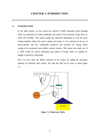
  • 1. 1 CHAPTER 1: INTRODUCTION 1.1 INTRODUCTION In our minor project, we have shown the concept of AMR (Automatic Meter Reading) which was purposed for remote monitoring and control of the domestic energy meter by GSM NET-WORK. This system enables the Electricity Department to read the meter reading regularly without the person visiting each house. It was achieved by the use of microcontroller unit that continuously monitored and recorded the Energy Meter reading in its permanent (non-volatile) memory location. This system also made use of a GSM model for remote monitoring and control of Energy meter by sending live reading to electricity department. Now we have done the further extension of the project by adding the preventive methods for electricity theft control. The main line theft can be done as shown figure 1.1. Figure 1.1 Main Line Thefts
  • 2. 2 1.2 MOTIVATION In India electricity theft leads to annual losses estimated at US$4.5 billion, about 1.5 percent of GDP. The motivation of this project is to protect electricity from being theft from the various methods like Tampering with meter seals, by-passing the meters, damaging or removing meters, illegal tapping to bare wires and illegal taps to low side of the transformer. The figure below shows the above methods of thefts in figure 1.2. Figure 1.2 Thefts method 1.3 OBJECTIVE This project presents detection of power theft in house and in industry for different methods of theft. Electrical energy is very important for everyday life and is the spine for the industry. In our daily life with increasing need of electricity the power theft is also increasing, power theft is a problem that continues to plague power sector across whole country the objective of this project is to design such a system, which will try to reduce the illegal use of electricity and reduce the chances of theft. This project will automatically collect the reading and detect the theft this model reduces manual manipulation work and try to achieves theft control. In this project, we use two current transformers to monitor the current status. One current sensor is connected to the main line and second sensor is connected to the main
  • 3. 3 house after meter. Meter show the reading of home. At the same time main line meter show the current status of different homes. If anybody hang the wires between pole and before meter then pole reading is to be exceed automatically and make a big difference between home reading and pole reading. If the difference is too much then circuit will automatically send a sms to the control room with theft message. 1.4 CIRCUIT DIAGRAM Figure 1.3 Circuit diagram of theft monitoring Figure 1.3 shows the circuit diagram of theft monitoring. It includes energy, meter load, step down transformer, reset circuitry, 89s52 microcontroller, GSM, LCD, MAX 232 IC, ADC, two current transformers. ADC converts analog signals to digital signals so that data can be fed to microcontroller. Microcontroller then analyse the data from both the current transformers and the data then can be send to authority by GSM.
  • 4. 4 CHAPTER 2: COMPONENTS USED 2.1 Current Transformer (C.T) : The current transformer is a type of "instrument transformer" that is designed to produce an alternating current in its secondary winding which is proportional to the current being measured in its primary. Current transformers reduce high voltage currents to a much lower value and provide a convenient way of safely monitoring the actual electrical current flowing in an AC transmission line using a standard ammeter. The principal of operation of a current transformer is no different from that of an ordinary transformer. The types of current transformer are shown in fig. 2.1. Figure 2.1 Typical Current Transformers Unlike the voltage or Power Transformer looked at previously, the current transformer consists of only one or very few turns as its primary winding. This primary winding can be of either a single flat turn, a coil of heavy duty wire wrapped around the core or just a conductor or bus bar placed through a central hole as shown. Due to this type of arrangement, the current transformer is often referred too as a "series transformer" as the primary winding, which never has more than a very few turns, is in series with the current carrying conductor. The secondary winding may have a large number of coil turns wound on a laminated core of low-loss magnetic material which has a large cross-sectional area so that the magnetic flux density is low using much smaller cross-sectional area wire, depending
  • 5. 5 upon how much the current must be stepped down. This secondary winding is usually rated at a standard 1 Ampere or 5 Amperes. The construction of current transformer is shown in figure 2.2. Figure 2.2 Constructions of current transformers There are three basic types of current transformers: "wound", "toroidal" and "bar". • Wound current transformers – The transformers primary winding is physically connected in series with the conductor that carries the measured current flowing in the circuit. The magnitude of the secondary current is dependent on the turns ratio of the transformer. • Toroidal current transformers – These do not contain a primary winding. Instead, the line that carries the current flowing in the network is threaded through a window or hole in the toroidal transformers. Some current transformers have a "split core" which allows it to be opened, installed, and closed, without disconnecting the circuit to which they are attached. • Bar-type current transformers – This type of current transformer uses the actual cable or bus-bar of the main circuit as the primary winding, which is equivalent to a single turn. They are fully insulated from the high operating voltage of the system and are usually bolted to the current carrying device. Current transformers can reduce or "step-down" current levels from thousands of amperes down to a standard output of a known ratio to either 5 Amps or 1 Amp for normal operation. Thus, small and accurate instruments and control devices can be used with CT's because they are insulated away from any high-voltage power lines. There are a variety of metering applications and uses for current transformers such as with
  • 6. 6 wattmeter's, power factor meters, watt-hours, protective relays, or as trip coils in magnetic circuit breakers, So for example, a current transformer with a relationship of say, 300/5A can be converted to another of 150/5A or even 100/5A by passing the main primary conductor through its interior window two or three times as shown. This allows a higher value current transformer to provide the maximum output current for the ammeter when used on smaller primary current lines. Current Transformer Primary Turns Ratio Figure 2.3 Turns ratio in C.T Example No. 1 A bar-type current transformer which has 1 turn on its primary and 160 turns on its secondary is to be used with a standard range of ammeters that have an internal resistance of 0.2Ω's. The ammeter is required to give a full scale deflection when the primary current is 800 Amps. Calculate the maximum secondary current and secondary voltage across the ammeter. Secondary Current: Voltage across Ammeter: We can see above that since the secondary of the current transformer is connected across the ammeter, which has a very small resistance, the voltage drop across the
  • 7. 7 secondary winding is only 1.0 volts at full primary current. If the ammeter is removed, the secondary winding becomes open-circuited and the transformer acts as a step-up transformer resulting in a very high voltage equal to the ratio of: Vp(Ns/Np) being developed across the secondary winding. So for example, assume our current transformer from above is connected to a 480 volt three-phase power line. Therefore: 2.2 89S52 MICROCONTROLLER 8051 is the name of a big family of microcontrollers. The device which we used in our project was the 'AT89S52' which is a typical 8051 microcontroller manufactured by Atmel™. The block diagram provided by Atmel™ in their datasheet that showed the architecture of 89S52 device seemed a bit complicated. A simpler architecture can be represented below. The 89S52 has 4 different ports, each one having 8 Input/output lines providing a total of 32 I/O lines. Those ports can be used to output DATA and orders do other devices, or to read the state of a sensor, or a switch. Most of the ports of the 89S52 have 'dual function' meaning that they can be used for two different functions. The first one is to perform input/output operations and the second one is used to implement special features of the microcontroller like counting external pulses, interrupting the execution of the program according to external events, performing serial data transfer or connecting the chip to a computer to update the software. Each port has 8 pins, and will be treated from the software point of view as an 8-bit variable called 'register', each bit being connected to a different Input/output pin. The pin diagram is shown in fig. 2.4.
  • 8. 8 Figure 2.4 Pin Diagram of 8051 Microcontroller The 8051 MICROCONTROLLER The 8051 developed and launched in the early 80`s, is one of the most popular micro controller in use today. It has a reasonably large amount of built in ROM and RAM. In addition it has the ability to access external memory. The generic term `8x51` is used to define the device. The value of x defining the kind of ROM, i.e. x=0, indicates none, x=3, indicates mask ROM, x=7, indicates EPROM and x=9 indicates EEPROM or Flash.  About ROM The early 8051, namely the 8031 was designed without any ROM. This device could run only with external memory connected to it. Subsequent developments lead to the development of the PROM or the programmable ROM. This type had the disadvantage of being highly unreliable. The next in line, was the EPROM or Erasable Programmable ROM. These devices used ultraviolet light erasable memory cells. Thus a program could be loaded, tested and erased using ultra violet rays. A new program could then be loaded again.
  • 9. 9 An improved EPROM was the EEPROM or the electrically erasable PROM. This does not require ultra violet rays, and memory can be cleared using circuits within the chip itself. Finally there is the FLASH, which is an improvement over the EEPROM. While the terms EEPROM and flash are sometimes used interchangeably, the difference lies in the fact that flash erases the complete memory at one stroke, and not act on the individual cells. This results in reducing the time for erasure.  Architecture Architecture is must to learn because before learning new machine it is necessary to learn the capabilities of the machine. This is something like before learning about the car you cannot become a good driver. The architecture of the 8051 is given below. The architecture of 8051 microcontroller is shown in fig. 2.4.  8-bit CPU (Consisting of the ‘A’ and ‘B’ registers) Most of the transactions within the microcontroller are carried out through the ‘A’ register, also known as the Accumulator. In addition all arithmetic functions are carried out generally in the ‘A’ register. There is another register known as the ‘B’ register, which is used exclusively for multiplication and division. Thus an 8-bit notation would indicate that the maximum value that can be input into these registers is ‘11111111’. Puzzled? The value is not decimal 111, 11,111! It represents a binary number, having an equivalent value of ‘FF’ in Hexadecimal and a value of 255 in decimal. Figure 2.5 Architecture of 8051 Microcontroller
  • 10. 10  4K on-chip ROM Once you have written out the instructions for the microcontroller, where do you put these instructions. Obviously you would like these instructions to be safe, and not get deleted or changed during execution. Hence you would load it into the ‘ROM’. The size of the program you write is bound to vary depending on the application, and the number of lines. The 8051 microcontroller gives you space to load up to 4K of program size into the internal ROM.4K, that’s all? Well just wait. You would be surprised at the amount of stuff you can load in this 4K of space. Of course you could always extend the space by connecting to 64K of external ROM if required.  128 bytes on-chip RAM This is the space provided for executing the program in terms of moving data, storing data etc.  32 I/O lines. (Four- 8 bit ports, labelled P0, P1, P2, P3) In our bulb example, we used the notation p1.0. This means bit zero of port one. One bit controls one bulb. Thus, port one would have 8 bits. There are a total of four ports named p0, p1, p2, p3, giving a total of 32 lines. These lines can be used both as input or output.  Two 16 bit timers / counters. A microcontroller normally executes one instruction at a time. However certain applications would require that some event has to be tracked independent of the main program. The manufacturers have provided a solution, by providing two timers. These timers execute in the background independent of the main program. Once the required time has been reached, (remember the time calculations described above?), they can trigger a branch in the main program. These timers can also be used as counters, so that they can count the number of events, and on reaching the required count, can cause a branch in the main program.  Full Duplex serial data receiver / transmitter. The 8051 microcontroller is capable of communicating with external devices like the PC etc. Here data is sent in the form of bytes, at predefined speeds, also known as baud
  • 11. 11 rates. The transmission is serial, in the sense, one bit at a time  5-Interrupt sources with two priority levels (Two external and three internal): During the discussion on the timers, we had indicated that the timers can trigger a branch in the main program. However, what would we do in case we would like the microcontroller to take the branch, and then return back to the main program, without having to constantly check whether the required time / count has been reached. This is where the interrupts come into play. These can be set to either the timers, or to some external events. Whenever the background program has reached the required criteria in terms of time or count or an external event, the branch is taken, and on completion of the branch, the control returns to the main program. Priority levels indicate which interrupt is more important, and needs to be executed first in case two interrupts occur at the same time.  On-chip clock oscillator. This represents the oscillator circuits within the microcontroller. Thus the hardware is reduced to just simply connecting an external crystal, to achieve the required pulsing rate. SPECIFICATIONS:  Core Processor: 8051  Data Bus Width: 8 bit  Maximum Clock Frequency: 33 MHz  Program Memory Size: 8 KB  Program Memory Type: Flash  RAM Size: 256 B  ADC: No  Number of Programmable I/Os: 32  Number of Timers: 3  Supply Voltage Range: 4 V to 5.5 V  Package: PDIP
  • 12. 12 2.3 Liquid crystal display A liquid crystal display (LCD) is a thin, flat display device made up of any number of color or monochrome pixels arrayed in front of a light source or reflector. It is prized by engineers because it uses very small amounts of electric power, and is therefore suitable for use in battery-powered electronic devices. The LCD is shown in fig. 2.5. Fig. 2.6 Reflective twisted pneumatic liquid crystal display. Descriptions of LCD as shown in Fig. 2.5 are as follows: 1. Vertical filter film to polarize the light as it enters. 2. Glass substrate with ITO electrodes. The shapes of these electrodes will determine the dark shapes that will appear when the LCD is turned on or off. Vertical ridges etched on the surface are smooth. 3. Twisted pneumatic liquid crystals. 4. Glass substrate with common electrode film (ITO) with horizontal ridges to line up with the horizontal filter. 5. Horizontal filter film to block/allow through light. 6. Reflective surface to send light back to viewer. 2.3.1 Overview Each pixel of an LCD consists of a layer of liquid crystal molecules aligned between two transparent electrodes, and two polarizing filters, the axes of polarity of which are perpendicular to each other. With no liquid crystal between the polarizing filters, light passing through one filter would be blocked by the other. The surfaces of the electrodes that are in contact with the liquid crystal material are treated so as to align the liquid crystal molecules in a particular direction. This treatment typically consists of a thin polymer layer that is unidirectional rubbed using a
  • 13. 13 cloth (the direction of the liquid crystal alignment is defined by the direction of rubbing). The diagram below in figure 2.6 showed a sub pixel of a colour LCD. Figure 2.7 A sub pixel of a color LCD Before applying an electric field, the orientation of the liquid crystal molecules is determined by the alignment at the surfaces. In a twisted pneumatic device (the most common liquid crystal device), the surface alignment directions at the two electrodes are perpendicular, and so the molecules arrange themselves in a helical structure, or twist. Because the liquid crystal material is bi fringe (i.e. light of different polarizations travels at different speeds through the material), light passing through one polarizing filter is rotated by the liquid crystal helix as it passes through the liquid crystal layer, allowing it to pass through the second polarized filter. Half of the light is absorbed by the first polarizing filter, but otherwise the entire assembly is transparent. When a voltage is applied across the electrodes, a torque acts to align the liquid crystal molecules parallel to the electric field, distorting the helical structure (this is resisted by elastic forces since the molecules are constrained at the surfaces). This reduces the rotation of the polarization of the incident light, and the device appears gray. If the applied voltage is large enough, the liquid crystal molecules are completely untwisted and the polarization of the incident light is not rotated at all as it passes through the liquid crystal layer. This light will then be polarized perpendicular to the second filter, and thus be completely blocked and the pixel will appear black. By controlling the voltage applied across the liquid crystal layer in each pixel, light can be allowed to pass through in varying amounts, correspondingly illuminating the pixel. With a twisted pneumatic liquid crystal device it is usual to operate the device between crossed
  • 14. 14 polarizer’s, such that it appears bright with no applied voltage. With this setup, the dark voltage-on state is uniform. The device can be operated between parallel polarizer’s, in which case the bright and dark states are reversed (in this configuration, the dark state appears blotchy). Both the liquid crystal material and the alignment layer material contain ionic compounds. If an electric field of one particular polarity is applied for a long period of time, this ionic material is attracted to the surfaces and degrades the device performance. This is avoided by applying either an alternating current, or by reversing the polarity of the electric field as the device is addressed (the response of the liquid crystal layer is identical, regardless of the polarity of the applied field). When a large number of pixels is required in a display, it is not feasible to drive each directly since then each pixel would require independent electrodes. Instead, the display is multiplexed. In a multiplexed display, electrodes on one side of the display are grouped and wired together (typically in columns), and each group gets its own voltage source. On the other side, the electrodes are also grouped (typically in rows), with each group getting a voltage sink. The groups are designed so each pixel has a unique, unshared combination of source and sink. The electronics or the software driving the electronics then turns on sinks in sequence, and drives sources for the pixels of each sink. Important factors to consider when evaluating an LCD monitor include resolution, viewable size, response time (sync rate), matrix type (passive or active), viewing angle, color support, brightness and contrast ratio, aspect ratio, and input ports (e.g. DVI or VGA). 2.3.2 Colour display In colour LCDs each individual pixel is divided into three cells, or sub pixels, which are colour red, green, and blue, respectively, by additional filters (pigment filters, dye filters and metal oxide filters). Each sub pixel can be controlled independently to yield thousands or millions of possible colours for each pixel. Older CRT monitors employ a similar method. Colour components may be arrayed in various pixel geometries, depending on the monitor's usage. If software knows which type of geometry is being used in a given
  • 15. 15 LCD, this can be used to increase the apparent resolution of the monitor through sub pixel rendering. This technique is especially useful for text anti-aliasing. A general purpose alphanumeric LCD, with two lines of 16 characters. LCDs with a small number of segments, such as those used in digital watches and pocket calculators, have a single electrical contact for each segment. An external dedicated circuit supplies an electric charge to control each segment. This display structure is unwieldy for more than a few display elements. Small monochrome displays such as those found in personal organizers, or older laptop screens have a passive-matrix structure employing supertwist pneumatic (STN) or double-layer STN (DSTN) technology (DSTN corrects a colour-shifting problem with STN). Each row or column of the display has a single electrical circuit. The pixels are addressed one at a time by row and column addresses. This type of display is called a passive matrix because the pixel must retain its state between refreshes without the benefit of a steady electrical charge. As the number of pixels (and, correspondingly, columns and rows) increases, this type of display becomes less feasible. Very slow response times and poor contrast are typical of passive-matrix LCDs. High-resolution color displays such as modern LCD computer monitors and televisions use an active matrix structure. A matrix of thin-film transistors (TFTs) is added to the polarizing and color filters. Each pixel has its own dedicated transistor, allowing each column line to access one pixel. When a row line is activated, all of the column lines are connected to a row of pixels and the correct voltage is driven onto all of the column lines. The row line is then deactivated and the next row line is activated. All of the row lines are activated in sequence during a refresh operation. Active-matrix displays are much brighter and sharper than passive-matrix displays of the same size, and generally have quicker response times, producing much better images. 2.3.3 LCD DETAIL Frequently, an 8051 program must interact with the outside world using input and output devices that communicate directly with a human being. One of the most common devices attached to an 8051 is an LCD display. Some of the most common LCDs connected to the 8051 are 16x2 and 20x2 displays. This means 16 characters per line by 2 lines and 20 characters per line by 2 lines, respectively.
  • 16. 16 Fortunately, a very popular standard exists which allows us to communicate with the vast majority of LCDs regardless of their manufacturer. The standard is referred to as HD44780U, which refers to the controller chip which receives data from an external source (in this case, the 8051) and communicates directly with the LCD. 44780 BACKGROUNDS The 44780 standard requires 3 control lines as well as either 4 or 8 I/O lines for the data bus. The user may select whether the LCD is to operate with a 4-bit data bus or an 8-bit data bus. If a 4-bit data bus is used, the LCD will require a total of 7 data lines (3 control lines plus the 4 lines for the data bus). If an 8-bit data bus is used, the LCD will require a total of 11 data lines (3 control lines plus the 8 lines for the data bus). The three control lines are referred to as EN, RS, and RW. The EN line is called "Enable." This control line is used to tell the LCD that you are sending it data. To send data to the LCD, your program should first set this line high (1) and then set the other two control lines and/or put data on the data bus. When the other lines are completely ready, bring EN low (0) again. The 1-0 transition tells the 44780 to take the data currently found on the other control lines and on the data bus and to treat it as a command. The RS line is the "Register Select" line. When RS is low (0), the data is to be treated as a command or special instruction (such as clear screen, position cursor, etc.). When RS is high (1), the data being sent is text data which should be displayed on the screen. For example, to display the letter "T" on the screen you would set RS high. The typical LCD is shown in figure 2.7. Figure 2.8 A typical LCD The RW line is the "Read/Write" control line. When RW is low (0), the information on the data bus is being written to the LCD. When RW is high (1), the program is
  • 17. 17 effectively querying (or reading) the LCD. Only one instruction ("Get LCD status") is a read command. All others are write commands--so RW will almost always be low. Finally, the data bus consists of 4 or 8 lines (depending on the mode of operation selected by the user). In the case of an 8-bit data bus, the lines are referred to as DB0, DB1, DB2, DB3, DB4, DB5, DB6, and DB7. 2.4 GSM GSM is a mobile communication modem; it is stands for global system for mobile communication (GSM). The idea of GSM was developed at Bell Laboratories in 1970. It is widely used mobile communication system in the world. GSM is an open and digital cellular technology used for transmitting mobile voice and data services operates at the 850MHz, 900MHz, 1800MHz and 1900MHz frequency bands. GSM system was developed as a digital system using time division multiple access (TDMA) technique for communication purpose. A GSM digitizes and reduces the data, then sends it down through a channel with two different streams of client data, each in its own particular time slot. The digital system has an ability to carry 64 kbps to 120 Mbps of data rates. The GSM SIM 900 is shown in figure 2.9. Figure 2.9 GSM SIM900 2.4.1 GSM Modem A GSM modem is a device which can be either a mobile phone or a modem device which can be used to make a computer or any other processor communicate over a network. A GSM modem requires a SIM card to be operated and operates over a network range subscribed by the network operator. It can be connected to a computer through serial, USB or Bluetooth connection.
  • 18. 18 A GSM modem can also be a standard GSM mobile phone with the appropriate cable and software driver to connect to a serial port or USB port on your computer. GSM modem is usually preferable to a GSM mobile phone. The GSM modem has wide range of applications in transaction terminals, supply chain management, security applications, weather stations and GPRS mode remote data logging. There are various cell sizes in a GSM system such as macro, micro, pico and umbrella cells. Each cell varies as per the implementation domain. There are five different cell sizes in a GSM network macro, micro, pico and umbrella cells. The coverage area of each cell varies according to the implementation environment. Time Division Multiple Access TDMA technique relies on assigning different time slots to each user on the same frequency. It can easily adapt to data transmission and voice communication and can carry 64kbps to 120Mbps of data rate. 2.4.2 GSM Architecture A GSM network consists of the following components:  A Mobile Station: It is the mobile phone which consists of the transceiver, the display and the processor and is controlled by a SIM card operating over the network.  Base Station Subsystem: It acts as an interface between the mobile station and the network subsystem. It consists of the Base Transceiver Station which contains the radio transceivers and handles the protocols for communication with mobiles. It also consists of the Base Station Controller which controls the Base Transceiver station and acts as a interface between the mobile station and mobile switching centre.  Network Subsystem: It provides the basic network connection to the mobile stations. The basic part of the Network Subsystem is the Mobile Service Switching Centre which provides access to different networks like ISDN, PSTN etc. It also consists of the Home Location Register and the Visitor Location Register which provides the call routing and roaming capabilities of GSM. It also contains the Equipment Identity Register which maintains an account of all the mobile equipments
  • 19. 19 wherein each mobile is identified by its own IMEI number. IMEI stands for International Mobile Equipment Identity. Features of GSM Module:  Improved spectrum efficiency  Compatibility with integrated services digital network (ISDN)  SIM phonebook management  Fixed dialing number (FDN)  Real time clock with alarm management  High-quality speech  Uses encryption to make phone calls more secure  Short message service (SMS) The security strategies standardized for the GSM system make it the most secure telecommunications standard currently accessible. Although the confidentiality of a call and secrecy of the GSM subscriber is just ensured on the radio channel, this is a major step in achieving end-to- end security. 2.5 Step-Down Transformer Step down transformer from 220 volt Ac to 9-0-9 AC. We use step down transformer to step down the voltage from 220 to 9 volt ac. This AC is further connected to the rectifier circuit for AC to DC conversion. Transformer current rating is 750 mA. The symbol of step down transformer is shown in fig.2.10. Figure 2.10 Step-down transformer
  • 20. 20 2.6 Reset Circuitry Pin no 9 of the controller is connected to the reset circuit. On the circuit we connect one resistor and capacitor circuit to provide a reset option when power is on. As soon as you give the power supply the 8051 doesn’t start. You need to restart for the microcontroller to start. Restarting the microcontroller is nothing but giving a Logic 1 to the reset pin at least for the 2 clock pulses. So it is good to go for a small circuit which can provide the 2 clock pulses as soon as the microcontroller is powered. We are just using a capacitor to charge the microcontroller and again discharging via resistor. The reset circuitry is shown in fig. 2.11. Figure 2.11 Reset Circuitry 2.7 Diode In this project we use IN 4007 diode as a rectifier. IN 4007 is special diode to convert the AC into DC In this project we use two diode as a rectifier. Here we use full wave rectifier. Output of rectifier is pulsating DC. To convert the pulsating dc into smooth dc we use Electrolytic capacitor as a main filter. Capacitor converts the pulsating dc into smooth dc and this DC is connected to the Regulator circuit for Regulated 5 volt DC. The diode and regulated IC is shown in fig. 2.12. Fig. 2.12 Regulated IC 7805(left side) and diode (right side)
  • 21. 21 Fig. 2.13 Connection of full wave rectifier circuit Pin no 40 of the controller is connected to the positive supply. Pin no 20 is connected to the ground. Pin no 9 is connected to external resistor capacitor to provide an automatic reset option when power is on. In fig.2.13 we can see connection of crystal oscillators. Figure 2.14 Connection of IC 89s51 to crystal oscillator. 2.8 Crystal Oscillator Pin no 18 and 19 is connected to external crystal oscillator to provide a clock to the circuit. Crystals provide the synchronization of the internal function and to the peripherals. Whenever ever we are using crystals we need to put the capacitor behind it to make it free from noises. It is good to go for a 33pf capacitor. The crystal oscillator is shown in fig. 2.15.
  • 22. 22 Fig. 2.15 Crystal oscillator We can also resonators instead of costly crystal which are low cost and external capacitor can be avoided. But the frequency of the resonators varies a lot. And it is strictly not advised when used for communications projects. Calculation time required. The speed with which a microcontroller executes instructions is determined by what is known as the crystal speed. A crystal is a component connected externally to the microcontroller. The crystal has different values, and some of the used values are 6MHZ, 10MHZ, and 11.059 MHz etc. Thus a 10MHZ crystal would pulse at the rate of 10,000,000 times per second. The time is calculated using the formula No of cycles per second = Crystal frequency in HZ / 12. For a 10MHZ crystal the number of cycles would be, 10,000,000/12=833333.33333 cycles. This means that in one second, the microcontroller would execute 833333.33333 cycles.
  • 23. 23 CHAPTER 3: INFRARED ALARM FOR METER TAMPERING 3.1 INFRA RED ALARM Infra red intruder alarm is a very good project to demonstrate the working of the burglar alarm. In this project when anybody interrupt the light then alarm is automatic on. For this purpose we use one infra red transmitter L.E.D and one infra red receiver diode as a receiver component. All this components is connected to the IC 555. IC 555 is an 8 pin IC. Pin no 4 and 8 is connected to the positive supply. Pin no 1 is connected to the negative voltage. Pin no 3 is a output pin. Pin no 2 is input trigger pin. Photodiode is connected to the pin no 2. One buzzer is connected to the pin no 3 via NPN transistor circuit. When light from the infra red led is focus on the photodiode then photodiode gives a low resistance and so that pin no 2 is become more positive. When pin no. 2 is become more positive then output is negative and so that buzzer is off at that time. When anybody interrupts the light then photodiode is in high resistance and photodiode is off at that time and pin no 2 is become more negative. Now at that time pin no 3 is on high voltage on base of the transistor and due to this NPN transistor switch on the buzzer circuit Pin no 6 and 7 of this IC is a time control pin. In this circuit there is no use of timer, so we connect very small value resistance and one capacitor to pin no 6 and 7.The PIN diagram of IC 555 is shown here in figure 3.1. Figure 3.1 IC 555
  • 24. 24 3.2 COMPONENT USED. 3.2.1 IC 555 AND 8 PIN BASE.  The 555 timer IC is an integral part of electronics projects. Be it a simple project involving a single 8 bit micro-controller and some peripherals or a complex one involving system on chips (SoCs), 555 timers working is involved. These provide time delays, as an oscillator and as a flip-flop element among other applications.  Introduced in 1971 by the American company Signetics, the 555 is still in widespread use due to its low price, ease of use and stability. It is made by many companies in the original bipolar and low-power CMOS types. According to an estimate, a billion units were manufactured back in the year 2003 alone. (That time, only 555 i knew was a cough syrup).  Depending on the manufacturer, the standard 555 package includes 25 transistors, 2 diodes and 15 resistors on a silicon chip installed in an 8-pin mini dual-in- line package (DIP-8). Variants consist of combining multiple chips on one board. However 555 are still the most popular. Some important features of the 555 timer: 555 are used in almost every electronic circuit today. For a 555 timer working as a flip flop or as a multi-vibrator, it has a particular set of configurations. Some of the major features of the 555 would be  It operates from a wide range of power ranging from +5 Volts to +18 Volts supply voltage.  Sinking or sourcing 200 mA of load current.  The external components should be selected properly so that the timing intervals can be made into several minutes along with the frequencies exceeding several hundred kilo hertz.  The output of a 555 timer can drive transistor-transistor logic (TTL) due to its high current output.  It has a temperature stability of 50 parts per million (ppm) per degree Celsius change in temperature which is equivalent to 0.005 % per °C.
  • 25. 25 3.2.2 INFRA RED L.E.D. An Infrared light emitting diode (IR LED) is a special purpose LED emitting infrared rays ranging 700 nm to 1 mm wavelength. Different IR LEDs may produce infrared light of differing wavelengths, just like different LEDs produce light of different colors. IR LEDs are usually made of gallium arsenide or aluminum gallium arsenide. In complement with IR receivers, these are commonly used as sensors. The appearance of IR LED is same as a common LED. Since the human eye cannot see the infrared radiations, it is not possible for a person to identify if an IR LED is working. A camera on a cell phone camera solves this problem. The IR rays from the IR LED in the circuit are shown in the camera. Figure 3.2 Infrared sensor 3.2.3 CAPACITOR--- 470 mfd, 0.1 mfd and RESISTANCE-1K OHM, 10K OHM, 470 OHM. 3.2.4 PHOTODIODE A photodiode is a semiconductor device that converts light into an electrical current. The current is generated when photons are absorbed in the photodiode. Photodiodes may contain optical filters, built-in lenses, and may have large or small surface areas. Figure 3.3 Photo diode symbol
  • 26. 26 3.2.5 NPN TRANSISTOR BC 548 The BC548 is a general-purpose NPN bipolar junction transistor commonly used in European and American electronic equipment. It is notably often the first type of bipolar transistor hobbyist’s encounter and is often featured in designs in hobby electronics magazines where a general-purpose transistor is required. The BC548 is a part of a family of NPN and PNP epitaxial silicon transistors that originated with the metal-cased BC108 family of transistors. The BC548 is the modern plastic-packaged BC108: the BC548 article at the Radio museum website describes the BC548 as a successor to the BC238 and differing from the BC108 in only the shape of the package. Datasheets for the BC548 give specifications that are identical to, or exceed, those of the BC108, BC148 and BC238 predecessors. Thus the BC548 (or BC546 to 550) is a valid substitute in any circuit designed for the older BC108 (or BC148), which includes many Mullard and Philips published designs. 3.3 CIRCUIT DIAGRAM Figure 3.4 INFRARED SENSOR
  • 27. 27 CHAPTER 4: THEFT CONTROL SYSTEM 4.1 INTRODUCTION – Theft Control In this project we use two current transformers for load measurement. For current measurement we use CT coil. We use 3200 turns ct coil. This coil is readily available in the market. In this ct coil there is two wires. These two wires are connected to the rectifier circuit. We use 4148 diode as a rectifier; we choose 4148 diode for specific reason. Forward bias voltage drop of the 4148 is approx .3 volts which is less then silicon diode. Output of the 4148 diode is further connected to the small electrolytic capacitor for smoothing. Capacitor converts the pulsating dc into smooth dc. Output of the rectifier is connected to the ADC circuit via variable resistor. Here we use 0809 ADC for analogue to digital conversion. We choose ADC 0809 for specific purpose. ADC 0809 has a 8 channel inputs with three address select pins. Pin no 26, 27 is here use for inputs. Three address pins are 23, 24, 25 which is connected to pin no 1, 2, 3 of the controller. ADC 0809 provides a parallel output with 8 bit resolution. Output from the ADC is from pin no 17, 14, 15, 8, 18, 19, 20, and 21. These 8 pins provide a output signal on ADC. This signal is further connected to the port 2 (pin no 21 to 28). Microcontroller gets the signal and converts into ASCII code. ASCII code is connected to the LCD display via port 0. We use 2 by 16 LCD. Pin no 2 of the LCD is connected to the positive 5 volt supply. Pin no 1, 16 of the LCD is connected to ground. Pin no 15 Figure 4.1 LCD connection
  • 28. 28 is connected to the positive 5 volt via series diode. Data from the controller is connected to the LCD data pin in parallel. Pin no 4, 5, 6 is control pin of the LCD. The LCD connection is shown below in figure 4.1. 4.2 STEALING The metering of electric energy meter is mainly according to the relationship with voltage, electric current and power factor angle. The behaviour of electricity stealing not only makes the power industry suffering huge financial losses but also threatens the main power supply security and reliability. According to the analysis, there are many electricity stealing trick about electric energy meter, the methods could be approximately divided into under voltage, under current, phase shifted and difference expansion to their principle. Some common tricks: Un-hooking technology will electricity stealing. Secretly destroy the lead sealing of electric energy meter, open voltage hook of terminal in junction box and make no electric current through all using quantity of electricity steal. One fire-one ground technology. Take the ground. Wire as naught line, generally take the water pipe or cal duct as ground wire, the risk is bigger (most dangerous). Violated wire connection. Loop of short electric current, which makes the electric energy meter shift slow. Cross meter to connect wire, added bypass to reel across electric energy meter, which makes no or less electric current through, stall or rear measurement. Exchange fire wire and zero wire. Reverse the in and out of fire. Make electric meter reverse by using external supply. Adopt hand generator with voltage and current output or inverter power supply to join into the electric meter, make the electric energy meter reverse rapidly (rarely used technique and dangerous) As in fig 7, Due to the kind of electricity stealing and actual demand of preventing electricity stealing, based on that equipment of electricity stealing with remote monitoring is designed, which not only monitors the time electricity stealing occur but also offers the electricity stealing quantity and sends SMS to the local field man to catch the thief with positive proof to handle lawbreakers with the behaviour of electricity stealing. 4.3 ANALOG TO DIGITAL CONVERTER From the name itself it is clear that it is a converter which converts the analog (continuously variable) signal to digital signal. This is really an electronic integrated circuit which directly converts the continuous form of signal to discrete form. It can be expressed as A/D or A-to-D or A-D or ADC. The input (analog) to this system can have
  • 29. 29 any value in a range and are directly measured. But for output (digital) of an N-bit A/D converter, it should have only 2N discrete values. This A/D converter is a linkage between the analog (linear) world of transducers and discreet world of processing the signal and handling the data. The digital to analog converter (DAC) carry out the inverse function of the ADC. The schematic representation of ADC is shown below IN FIG. 4.2. Figure 4.2 schematic representation of ADC ADC Process There are mainly two steps involves in the process of conversion. They are:-  Sampling and Holding  Quantizing and Encoding The whole ADC conversion process is shown in figure 4.3. Figure 4.3 ADC conversion process Sampling and Holding In the process of Sample and hold (S/H), the continuous signal will gets sampled and freeze (hold) the value at a steady level for a particular least period of time. It is done to remove variations in input signal which can alter the conversion process and thereby
  • 30. 30 increases the accuracy. The minimum sampling rate has to be two times the maximum data frequency of the input signal. Quantizing and Encoding For understanding quantizing, we can first go through the term Resolution used in ADC. It is the smallest variation in analog signal that will result in a variation in the digital output. This actually represents the quantization error. V → Reference voltage range 2N → Number of states N → Number of bits in digital output Quantizing: It is the process in which the reference signal is partitioned into several discrete quanta and then the input signal is matched with the correct quantum. Encoding: Here; for each quantum, a unique digital code will be assigned and after that the input signal is allocated with this digital code. The process of quantizing and encoding is demonstrated in the table below. Table 4.1 analog to digital data From the above table we can observe that only one digital value is used to represent the whole range of voltage in an interval. Thus, an error will occur and it is called quantization error. This is the noise introduced by the process of quantization. Here the maximum quantization error is Improvement of Accuracy in ADC Two important methods are used for improving the accuracy in ADC. They are by increasing the resolution and by increasing the sampling rate. This is shown in figure below fig. 4.4.
  • 31. 31 Figure 4.4 sampling Types of Analog to Digital Converter  Successive Approximation ADC: This converter compares the input signal with the output of an internal DAC at each successive step. It is the most expensive type.  Dual Slope ADC: It have high accuracy but very slow in operation.  Pipeline ADC: It is same as that of two step Flash ADC.  Delta-Sigma ADC: It has high resolution but slow due to over sampling.  Flash ADC: It is the fastest ADC but very expensive.  Other: Staircase ramp, Voltage-to-Frequency, Switched capacitor, tracking, Charge balancing, and resolver. Application of ADC  Used together with the transducer.  Used in computer to convert the analog signal to digital signal.  Used in cell phones.  Used in microcontrollers.  Used in digital signal processing.  Used in digital storage oscilloscopes.  Used in scientific instruments.  Used in music reproduction technology etc.
  • 32. 32 4.3.1 Circuit diagram Figure 4.5 ADC pin diagram 4.4 MAX 232 The MAX232 is an integrated circuit first created in 1987 by Maxim Integrated Products that converts signals from a TIA-232 (RS-232) serial port to signals suitable for use in TTL-compatible digital logic circuits. The MAX232 is a dual transmitter / dual receiver that typically is used to convert the RX, TX, CTS, RTS signals. The drivers provide TIA-232 voltage level outputs (about ±7.5 volts) from a single 5- volt supply by on-chip charge pumps and external capacitors. This makes it useful for implementing TIA-232 in devices that otherwise do not need any other voltages. The receivers reduce TIA-232 inputs, which may be as high as ±25 volts, to standard 5 volt TTL levels. These receivers have a typical threshold of 1.3 volts and a typical hysteresis of 0.5 volts. The MAX232 replaced an older pair of chips MC1488 and MC1489 that performed similar RS-232 translation. The MC1488 quad transmitter chip required 12 volt and -12 volt power,[1] and MC1489 quad receiver chip required 5 volt power.[2] The main disadvantages of this older solution was the +/- 12 volt power requirement, only supported 5 volt digital logic, and two chips instead of one. Controller output is connected to the GSM modem serially via MAS232 IC. We use max232 IC is convert TTL data to RS232. Here we use sim300/sim900 GSM modem at the baud rate of 9600.
  • 33. 33 Figure 4.6 RS MAX 232 4.4.1 VOLTAGE LEVELS The MAX232 translates a TTL logic 0 input to between +3 and +15 V, and changes TTL logic 1 input to between −3 and −15 V, and vice versa for converting from TIA-232 to TTL. Table 4.2: Voltage Level Description of MAX RS 232 TIA-232 line type and logic level TIA-232 voltage TTL voltage to/from MAX232 Data transmission (Rx/Tx) logic 0 +3 V to +15 V 0 V Data transmission (Rx/Tx) logic 1 −3 V to −15 V 5 V Control signals (RTS/CTS/DTR/DSR) logic 0 −3 V to −15 V 5 V Control signals (RTS/CTS/DTR/DSR) logic 1 +3 V to +15 V 0 V
  • 34. 34 4.4.2 Applications The MAX232 (A) has two receivers that convert from RS-232 to TTL voltage levels, and two drivers that convert from TTL logic to RS-232 voltage levels. As a result, only two out of all RS-232 signals can be converted in each direction. Typically, the first driver/receiver pair of the MAX232 is used for TX and RX signals, and the second one for CTS and RTS signals. There are not enough drivers/receivers in the MAX232 to also connect the DTR, DSR, and DCD signals. Usually, these signals can be omitted when, for example, communicating with a PC's serial interface, or when special cables render them unnecessary. If the DTE requires these signals, a second MAX232 or some other IC from the MAX232 family can be used. Figure 4.7 max RS 232
  • 35. 35 CHAPTER 5: RESULT AND DISCUSSION Advanced metering systems can provide benefits for utilities, retail providers and customers. Benefits will be recognized by the utilities with increased efficiencies, outage detection, tamper notification and reduced labour cost as a result of automating reads, connections and disconnects. Retail providers will be able to offer new innovative products in addition to customizing packages for their customers. In addition, with the meter data being readily available, more flexible billing cycles would be available to their customers instead of following the standard utility read cycles. With timely usage information available to the customer, benefits will be seen through opportunities to manage their energy consumption and change from one REP to another with actual meter data. Because of these benefits, many utilities are moving towards implementing some types of AMR solutions. The government saves money by the control of theft in energy meter and also more beneficial for customer side and the government side. The metering IC ensures the accurate and reliable measurement of power consumed. Cost wise low when compared to other energy meter without automatic meter reading and theft control. The benefits of smart metering for the utility  Accurate meter reading, no more estimates  Improved billing  Accurate profile classes and measurement classes, true costs applied  Improved security and tamper detection for equipment. Disadvantages of automatic meter reading  Utility can possibly control amount allocated to users.  Risk of loss of privacy - details of use reveal information about user activities.  Greater potential for monitoring by other/unauthorized third parties.
  • 36. 36 CHAPTER 6: CONCLUSION We have studied RF based automatic meter used in different places. We got that this technology is very useful in present and future demand. AMR served well for commercial and industrial accounts. The AMR enable us to save million of dollar every year in meter reading cost and also provide our customer with better information about electricity, more accurate billing and keep rates as low as we can. The project model reduces the manual manipulation work and electricity theft .Use of GSM in our system provides the numerous advantages of wireless network systems. The government can save money by the control of theft in energy meter and more beneficial for customer side and the government side. The metering IC ensures the accurate and reliable measurement of power consumed. What was once needed for monthly data became a need for daily and even hourly reading of the meter. AMR as a way of improving customer service while reducing the cost of reading meter. Cost wise low when compared to other energy meter without automatic meter reading and theft control. The development of GSM based energy meter demonstrates the concept and implementation of new power metering system. GSM based AMR have low infrastructure cost, low operating costs, more data security and less man power required. It not only solve the problem of manual meter reading but also provide additional feature such as power disconnect, power connect , power cut alert and tempering alert customer can also pay bill via online login on authenticated web. Data base server can stored the current month data and also all previous month data for future use. So it saves a lot amount of time and energy.
  • 37. 37 REFERENCES [1] Netlab.cs.iitm.ernet.in/cs648/2009/tpf/cs09s022.pdf. [2] (Online resources-basic electronics), https://electronicsforu.com/resources/learn- electronics/ , electronics for you (monthly magazine). [3] Smart and Intelligent GSM based Automatic MeterReading System, International Journal of Engineering Research & Technology (IJERT),Vol. 1 Issue 3, ISSN: 2278- 0181, May – 2012. [4] International Journal of Computer Applications (0975 – 8887) Volume 116 – No. 18, April 2015. [5] Bharat Kulkarni,”GSM Based Automatic Meter Reading System Using ARM Controller”,International Journal of Emerging Technology and Advanced Engineering, ISSN 2250-2459, Volume 2, Issue 5, pp.446-448,May 2012. [6] PLC (Power Line Communication) Introduction, www.eetimes.com/document.asp?doc_id=1279014 [7] http://www.itnews.com.au/News/160398,auditor-general-slams-victorian-smart- meters.aspx [8] https://en.wikipedia.org/wiki/Automatic_meter_reading#See_also [9] Amin S. Mehmood, T. Choudhry, M.A. Hanif, “A Reviewing the Technical Issues for the Effective Construction of Automatic Meter Reading System” in International Conference on Microelectronics, 2005 IEEE
  • 38. 38 APPENDIX AN EXAMPLE HARDWARE CONFIGURATION As we've mentioned, the LCD requires either 8 or 11 I/O lines to communicate with. For the sake of this tutorial, we are going to use an 8-bit data bus--so we'll be using 11 of the 8051's I/O pins to interface with the LCD. Figure 1 LCD connection As you can see, we've established a 1-to-1 relation between a pin on the 8051 and a line on the 44780 LCD. Thus as we write our assembly program to access the LCD, we are going to equate constants to the 8051 ports so that we can refer to the lines by their 44780 name as opposed to P0.1, P0.2, etc. Let's go ahead and write our initial equates: DB0 EQU P1.0 DB1 EQU P1.1 DB2 EQU P1.2 DB3 EQU P1.3 DB4 EQU P1.4 DB5 EQU P1.5 DB6 EQU P1.6 DB7 EQU P1.7 EN EQU P3.7 RS EQU P3.6
  • 39. 39 RW EQU P3.5 DATA EQU P1 Having established the above equates, we may now refer to our I/O lines by their 44780 name. For example, to set the RW line high (1), we can execute the following insutrction: SETB RW HANDLING THE EN CONTROL LINE As we mentioned above, the EN line is used to tell the LCD that you are ready for it to execute an instruction that you've prepared on the data bus and on the other control lines. Note that the EN line must be raised/lowered before/after each instruction sent to the LCD regardless of whether that instruction is read or write, text or instruction. In short, you must always manipulate EN when communicating with the LCD. EN is the LCD's way of knowing that you are talking to it. If you don't raise/lower EN, the LCD doesn't know you're talking to it on the other lines. Thus, before we interact in any way with the LCD we will always bring the EN line high with the following instruction: SETB EN And once we've finished setting up our instruction with the other control lines and data bus lines, we'll always bring this line back low: CLR EN CHECKING THE BUSY STATUS OF THE LCD As previously mentioned, it takes a certain amount of time for each instruction to be executed by the LCD. The delay varies depending on the frequency of the crystal attached to the oscillator input of the 44780 as well as the instruction which is being executed. While it is possible to write code that waits for a specific amount of time to allow the LCD to execute instructions, this method of "waiting" is not very flexible. If the crystal frequency is changed, the software will need to be modified. Additionally, if the LCD itself is changed for another LCD which, although 44780 compatible, requires more time to perform its operations, the program will not work until it is properly modified.
  • 40. 40 A more robust method of programming is to use the "Get LCD Status" command to determine whether the LCD is still busy executing the last instruction received. The "Get LCD Status" command will return to us two tidbits of information; the information that is useful to us right now is found in DB7. In summary, when we issue the "Get LCD Status" command the LCD will immediately raise DB7 if it's still busy executing a command or lower DB7 to indicate that the LCD is no longer occupied. Thus our program can query the LCD until DB7 goes low, indicating the LCD is no longer busy. At that point we are free to continue and send the next command. Since we will use this code every time we send an instruction to the LCD, it is useful to make it a subroutine. Let's write the code: WAIT_LCD: SETB EN :- Start LCD command CLR RS :- It's a command SETB RW :- It's a read command MOV DATA,#0FFh :-Set all pins to FF initially MOV A,DATA :- Read the return value JB ACC.7,WAIT_LCD :- If bit 7 high, LCD still busy CLR EN :- Finish the command CLR RW :- Turn off RW for future commands RET Thus, our standard practice will be to send an instruction to the LCD and then call our WAIT_LCD routine to wait until the instruction is completely executed by the LCD. This will assure that our program gives the LCD the time it needs to execute instructions and also makes our program compatible with any LCD, regardless of how fast or slow it is. INITIALIZING THE LCD Before you may really use the LCD, you must initialize and configure it. This is accomplished by sending a number of initialization instructions to the LCD. The first instruction we send must tell the LCD whether we'll be communicating with it with an 8-bit or 4-bit data bus. We also select a 5x8 dot character font. These two options are selected by sending the command 38h to the LCD as a command. As you will recall from the last
  • 41. 41 section, we mentioned that the RS line must be low if we are sending a command to the LCD. Thus, to send this 38h command to the LCD we must execute the following 8051 instructions: SETB EN CLR RS MOV DATA,#38h CLR EN LCALL WAIT_LCD We've now sent the first byte of the initialization sequence. The second byte of the initialization sequence is the instruction 0Eh. Thus we must repeat the initialization code from above, but now with the instruction. Thus the next code segment is: SETB EN CLR RS MOV DATA,#0Eh CLR EN LCALL WAIT_LCD The last byte we need to send is used to configure additional operational parameters of the LCD. We must send the value 06h. SETB EN CLR RS MOV DATA,#06h CLR EN LCALL WAIT_LCD INIT_LCD: SETB EN CLR RS MOV DATA,#38h CLR EN LCALL WAIT_LCD SETB EN CLR RS MOV DATA,#0Eh
  • 42. 42 CLR EN LCALL WAIT_LCD SETB EN CLR RS MOV DATA,#06h CLR EN LCALL WAIT_LCD RET Having executed this code the LCD will be fully initialized and ready for us to send display data to it. CLEARING THE DISPLAY When the LCD is first initialized, the screen should automatically be cleared by the 44780 controller. However, it's always a good idea to do things yourself so that you can be completely sure that the display is the way you want it. Thus, it's not a bad idea to clear the screen as the very first opreation after the LCD has been initialized. An LCD command exists to accomplish this function. Not suprisingly, it is the command 01h. Since clearing the screen is a function we very likely will wish to call more than once, it's a good idea to make it a subroutine: CLEAR_LCD: SETB EN CLR RS MOV DATA,#01h CLR EN LCALL WAIT_LCD RET How that we've written a "Clear Screen" routine, we may clear the LCD at any time by simply executing an LCALL CLEAR_LCD. WRITING TEXT TO THE LCD Once again, writing text to the LCD is something we'll almost certainly want to do over and over--so let's make it a subroutine.
  • 43. 43 WRITE_TEXT: SETB EN SETB RS MOV DATA,A CLR EN LCALL WAIT_LCD RET The WRITE_TEXT routine that we just wrote will send the character in the accumulator to the LCD which will, in turn, display it. Thus to display text on the LCD all we need to do is load the accumulator with the byte to display and make a call to this routine. Pretty easy, huh? A "HELLO WORLD" PROGRAM Now that we have all the component subroutines written, writing the classic "Hello World" program--which displays the text "Hello World" on the LCD is a relatively trivial matter. Consider: LCALL INIT_LCD LCALL CLEAR_LCD MOV A,#'H' LCALL WRITE_TEXT MOV A,#'E' LCALL WRITE_TEXT MOV A,#'L' LCALL WRITE_TEXT MOV A,#'L' LCALL WRITE_TEXT MOV A,#'O' LCALL WRITE_TEXT MOV A,#' ' LCALL WRITE_TEXT MOV A,#'W' LCALL WRITE_TEXT MOV A,#'O' LCALL WRITE_TEXT
  • 44. 44 MOV A,#'R' LCALL WRITE_TEXT MOV A,#'L' LCALL WRITE_TEXT MOV A,#'D' LCALL WRITE_TEXT The above "Hello World" program should, when executed, initialize the LCD, clear the LCD screen, and display "Hello World" in the upper left-hand corner of the display. PIN WISE DETAIL OF LCD 1. Vss GROUND 2. Vcc +5VOLT SUPPLY 3 Vee POWER SUPPLY TO CONTROL CONTRAST 4. RS RS = 0 TO SELECT COMMAND REGISTER RS = 1 TO SELECT DATA REGISTER 5. R/W R/W = 0 FOR WRITE R/W = 1 FOR READ 6 E ENABLE 7 DB0 8 DB1 9. DB2 10. DB3 11. DB4 12. DB5 13. DB6 14. DB7 15, 16 FOR BACK LIGHT DISPLAY