SlideShare a Scribd company logo
1 of 62
MICROPROCESSOR
& MICROCONTROLLER APPLICATIONS
54 EC 51
Lecture 5b – 8085 ALP & TIMING DIAGRAM
By DICKSON NKONGO, MSc.
ECE Department
MP & MC APPLICATIONS
Lecture 5b – 8085 ALP & Timing Diagram
Mr.DicksonNkongo:SJUCET--2017/2018
MACHINE CYCLES And Their Timing OF 8085:
MP & MC APPLICATIONS
Lecture 5 – 8085 ALP & Timing Diagram
As far as execution of instructions is concerned, in
8085 microprocessor, each instruction is divided into
two parts:
1- The operation code(opcode) and
2 - The operand
The opcode tells us what the operation is and the
operand is the necessary information required for the
instruction. The operand may be either data or an
address or other information required for the
instruction.
Each instruction is divided into machine cycles and
each machine cycle is divided into clock cycles or T-
states
Mr.DicksonNkongo:SJUCET--2017/2018
MP & MC APPLICATIONS
Lecture 5 – 8085 ALP & Timing Diagram
MACHINE CYCLES And Their Timing OF
8085:
During normal operation, the microprocessor
sequentially fetches, decodes and executes one
instruction after another until a halt instruction
(HALT).
Timing Diagram is the graphical representation
of the time taken for the execution of each
instruction by a microprocessor.
The execution time is represented in T-states.
Mr.DicksonNkongo:SJUCET--2017/2018
MACHINE CYCLES And Their Timing OF 8085:
MP & MC APPLICATIONS
Lecture 5 – 8085 ALP & Timing Diagram
Instruction Cycle:
Is the time required to execute an instruction
Machine Cycle:
The time required to access the memory or
input/output devices is called machine cycle.
T-State:
The machine cycle and instruction cycle takes
multiple clock periods.
A portion of an operation carried out in one
system clock period is called as T-state.
Mr.DicksonNkongo:SJUCET--2017/2018
• Clock Signal
The 8085 divides the clock frequency provided at X1 and
X2 inputs by 2 which is called operating frequency.
One T-state is equal to the time period of the internal
clock signal of the microprocessor
For Ex: If the internal clock frequency of 8085
microprocessor is 3 MHZ, One T-state is equal to
•
𝟏
𝒇
=
𝟏
𝟑𝒙𝟏𝟎 𝟔 = 0.333x10⁻⁶sec=333x10-9sec
• (333 nano seconds nearly)
MP & MC APPLICATIONS
Lecture 5 – 8085 ALP & Timing Diagram
Mr.DicksonNkongo:SJUCET--2017/2018
• Clock Signal
T-State
1 Clock cycle
Rise time and fall time
MP & MC APPLICATIONS
Lecture 5 – 8085 ALP & Timing Diagram
Mr.DicksonNkongo:SJUCET--2017/2018
• Single Signal
Single signal status is represented by a line. It may
have status either logic 0 or logic 1 or tri-state
Logic 0
Logic 1
Tri state
MP & MC APPLICATIONS
Lecture 5 – 8085 ALP & Timing Diagram
Mr.DicksonNkongo:SJUCET--2017/2018
• Group of signals
Group of signals is also called a bus.
Eg: Address bus, data bus
State changes
Valid state
Tri state
MP & MC APPLICATIONS
Lecture 5 – 8085 ALP & Timing Diagram
Mr.DicksonNkongo:SJUCET--2017/2018
MP & MC APPLICATIONS
Lecture 5 – 8085 ALP & Timing Diagram
Mr.DicksonNkongo:SJUCET--2017/2018
Machine cycle 2 Machine cycle 5
Instruction cycle
T – State 1 T – State 2 T – State 3 T – State 6
MP & MC APPLICATIONS
Lecture 5 – 8085 ALP & Timing Diagram
Machine cycle 1
Mr.DicksonNkongo:SJUCET--2017/2018
The 8085 microprocessor has 5 basic machine
cycles. They are
1. Opcode fetch cycle (4T)
2. Memory write cycle (3T)
3. I/O read cycle (3T)
4. Memory read cycle (3T)
5. I/O write cycle (3T)
Some more machine cycles for 8085:
1. Interrupt Acknowledge
2. Bus Idle
MP & MC APPLICATIONS
Lecture 5b – 8085 ALP & Timing Diagram
Mr.DicksonNkongo:SJUCET--2017/2018
8085 Machine Cycles
The three status signals IO/M*, S1 and S2 identify each
type
DICKSON NKONGO, MSc. : ECE Department.
MP & MC APPLICATIONS
Lecture 5b – 8085 ALP & Timing Diagram
Mr.DicksonNkongo:SJUCET--2017/2018
The Control and Status Signals
•There are 4 main control and status signals. These are:
• ALE: Address Latch Enable. This signal is a pulse that become
1 when the AD0 – AD7 lines have an address on them. It
becomes 0 after that. This signal can be used to enable a
latch to save the address bits from the AD lines.
• RD’: Read. Active low indicates that the data must be read
from the selected memory location or I/O port via data bus.
• WR’: Write. Active low indicates that the data must be
written into the selected memory location or I/O port via
data bus..
• IO/M’: This signal specifies whether the operation is a
memory operation (IO/M=0) or an I/O operation (IO/M=1).
• S1 and S0: Status signals to specify the kind of operation
being performed .Usually un-used in small systems.
DICKSON NKONGO, MSc. : ECE Department.
MP & MC APPLICATIONS
Lecture 5b – 8085 ALP & Timing Diagram
Mr.DicksonNkongo:SJUCET--2017/2018
Signal Timings
ALE
 This signal is active high signal. It is activated in the
beginning of T1 state of each machine cycle except
bus idle machine cycle and it remains active in the T1
state
DICKSON NKONGO, MSc. : ECE Department.
MP & MC APPLICATIONS
Lecture 5b – 8085 ALP & Timing Diagram
Mr.DicksonNkongo:SJUCET--2017/2018
Signal Timings
MP & MC APPLICATIONS
Lecture 5b – 8085 ALP & Timing Diagram
A0 - A7 (Lower Byte Address)
This is available on the multiplexed address/data bus (AD0 -
AD7) during T1 state of each machine cycle except bus idle
machine cycle.
Mr.DicksonNkongo:SJUCET--2017/2018
Signal Timings
MP & MC APPLICATIONS
Lecture 5b – 8085 ALP & Timing Diagram
D0 - D7 (Data Bus)
The data from memory or I/O device and from
microprocessor to memory or I/O device is transferred
during T2 and T3 – states.
N.B: In read machine cycle, data will appear on the
data bus during the later part of the T2 - state as shown
in fig. (next slide).
This is because to read data from memory or I/O device
it is necessary to select memory or I/O device, after the
selection, device will put the data from the selected
location on the data bus. This action needs finite time.
This time is referred as “Access Time”.
Mr.DicksonNkongo:SJUCET--2017/2018
Signal Timings
MP & MC APPLICATIONS
Lecture 5b – 8085 ALP & Timing Diagram
D0 - D7 (Data Bus)
In case of write cycle, data is available in the register set
of the microprocessor and it can put that data on the
data bus with zero access time.
Read Write
Mr.DicksonNkongo:SJUCET--2017/2018
Signal Timings
MP & MC APPLICATIONS
Lecture 5b – 8085 ALP & Timing Diagram
A8 - A15 (Higher Byte Address)
 The higher byte of address is available on the A8 –
A15 bus during T1, T2, and T3 – state of each
machine cycle, except bus idle machine cycle
Mr.DicksonNkongo:SJUCET--2017/2018
Signal Timings
MP & MC APPLICATIONS
Lecture 5b – 8085 ALP & Timing Diagram
IO/M*, S0, S1:
 These are called status signals. They decide the type of
machine cycle to be executed. They are activated at the
beginning of T1 – state of each machine cycle and remain
active till the end of the machine cycle
Mr.DicksonNkongo:SJUCET--2017/2018
Signal Timings
MP & MC APPLICATIONS
Lecture 5b – 8085 ALP & Timing Diagram
RD* and WR* (‘*’ here denotes Bar)
These decide the direction of the data transfer.
When RD* signal is active, data is transmitted
from memory or I/O device to microprocessor.
When WR* signal is active, data is transmitted
from microprocessor to the memory or I/O device.
Both signals are never active at a time.
**And since the data transfer in 8085 takes place
during T2 and T3, these signals are activated
during T2 and T3 as shown in the next slide
Mr.DicksonNkongo:SJUCET--2017/2018
RD* and WR*
DICKSON NKONGO, MSc. : ECE Department.
MP & MC APPLICATIONS
Lecture 5b – 8085 ALP & Timing Diagram
Mr.DicksonNkongo:SJUCET--2017/2018
• 8085 Machine cycles
MP & MC APPLICATIONS
Lecture 5b – 8085 ALP & Timing Diagram
Mr.DicksonNkongo:SJUCET--2017/2018
The Control and Status Signals
• (* ) means ‘bar’ i.e. active low
IO/M* RD* WR* REMARKS
0 0 1 Reading from memory
0 1 0 Writing into memory
1 0 1 Reading from IO device
1 1 0 Writing into IO device
X 1 1
No communication with
peripheral
DICKSON NKONGO, MSc. : ECE Department.
MP & MC APPLICATIONS
Lecture 5b – 8085 ALP & Timing Diagram
Mr.DicksonNkongo:SJUCET--2017/2018
The 8085 microprocessor has 5 basic machine
cycles. They are
1. Opcode fetch cycle (4T)
2. Memory write cycle (3T)
3. I/O read cycle (3T)
4. Memory read cycle (3T)
5. I/O write cycle (3T)
Some more machine cycles for 8085:
1. Interrupt Acknowledge
2. Bus Idle
MP & MC APPLICATIONS
Lecture 5b – 8085 ALP & Timing Diagram
Mr.DicksonNkongo:SJUCET--2017/2018
1. Opcode Fetch Machine Cycle
• The first step of executing any instruction is the Opcode
fetch cycle.
– In this cycle, the microprocessor brings in the
instruction’s Opcode from memory.
• To differentiate this machine cycle from the very
similar “memory read” cycle, the control & status
signals are set as follows:
– IO/M’=0, s0 and s1 are both 1.
– This machine cycle has four T-states.
• The 8085 uses the first 3 T-states to fetch the opcode.
• T4 is used to decode and execute it.
– It is also possible for an instruction to have 6 T-states in
an opcode fetch machine cycle.
MP & MC APPLICATIONS
Lecture 5b – 8085 ALP & Timing Diagram
Mr.DicksonNkongo:SJUCET--2017/2018
Machine Cycles
MP & MC APPLICATIONS
Lecture 5b – 8085 ALP & Timing Diagram
1. Opcode Fetch Machine Cycle:
Step 1: (State T1)
The 8085 places the contents of PC (Program
counter) on the address bus. Higher-order byte of
the PC is placed on the A8-A15 lines, while lower-
order on AD0-AD7 lines which stays on only
during T1.
Microprocessor activates ALE which is used to
latch the low-order byte of the address before it
disappears.
8085 also sends status signals IO/M* = 0, S1=1
and S0 = 1.
Mr.DicksonNkongo:SJUCET--2017/2018
Machine Cycles
MP & MC APPLICATIONS
Lecture 5b – 8085 ALP & Timing Diagram
1. Opcode Fetch Machine Cycle:
Step 2: (State T2)
Lower-byte address disappears from the AD0-
AD7 lines. However A0-A7 remain available as
they were latched during T1.
8085 sends RD* signal low to enable the
addressed memory location.
Then memory device places the contents of the
addressed memory location on the data bus
(AD0-AD7).
Mr.DicksonNkongo:SJUCET--2017/2018
Machine Cycles
MP & MC APPLICATIONS
Lecture 5b – 8085 ALP & Timing Diagram
1. Opcode Fetch Machine Cycle:
Step 3: (State T3)
8085 loads the data (opcode in this case) from
the data bus in its Instruction register.
Then raises RD* to high which disables the
memory device (deactivate RD signal)
Mr.DicksonNkongo:SJUCET--2017/2018
Machine Cycles
MP & MC APPLICATIONS
Lecture 5b – 8085 ALP & Timing Diagram
1. Opcode Fetch Machine Cycle:
Step 4: (State T4)
Microprocessor decodes the opcode, and on the
basis of the instruction received, it decides
whether to enter state T5 or to enter state T1 of
the next machine cycle.
One byte instructions which operates on eight bit
data (8 bit operand) are executed in T4. (e.g.
MOV A, B, ANA D, ADD C). This is because for
one byte instructions which operate on eight bit
data, data is always available in the internal
memory of 8085 i.e. registers
Mr.DicksonNkongo:SJUCET--2017/2018
Machine Cycles
MP & MC APPLICATIONS
Lecture 5b – 8085 ALP & Timing Diagram
1. Opcode Fetch Machine Cycle:
Step 5: (State T5 and T6)
Used for internal microprocessor operations
required by the instruction.
One byte instructions which operates on
sixteen bit data (16 bit operand) are executed
in T5 and T6. (e.g. DCX H, PCHL, SPHL,
INX H etc.
Mr.DicksonNkongo:SJUCET--2017/2018
Timing Diagram for Opcode Fetch Machine Cycle
MP & MC APPLICATIONS
Lecture 5 – 8085 ALP & Timing Diagram
Mr.DicksonNkongo:SJUCET--2017/2018
Timing Diagram for Opcode Fetch Machine Cycle
MP & MC APPLICATIONS
Lecture 5 – 8085 ALP & Timing Diagram
Timing Diagram for Opcode Fetch Machine Cycle
State T1
IO/M*=0, S1=1, S0=1
State T2
.
.
RD* = 0
Data
State T3
RD* = 1
State T4
Opcode
Decoded
(b)Timing Diagram for Opcode Fetch Machine Cycle
MP & MC APPLICATIONS
Lecture 5 – 8085 ALP & Timing Diagram
Machine Cycles
MP & MC APPLICATIONS
Lecture 5b – 8085 ALP & Timing Diagram
2. Memory Read Cycle:
 8085 executes this cycle to read the contents of R/W
memory (RAM) or ROM.
 The length of this machine cycle is 3-T states (T1-
T3).
Step 1: (State T1)
Microprocessor places the address on the address
lines from stack pointer, general purpose register
pair or program counter and then activates the
ALE signal for latching the low-byte of address.
Also microprocessor sends status signals: IO/M* =
0, S1 = 1, and S0 = 0 (for memory read machine
cycle)
Mr.DicksonNkongo:SJUCET--2017/2018
Machine Cycles
MP & MC APPLICATIONS
Lecture 5b – 8085 ALP & Timing Diagram
2. Memory Read Cycle:
Step 2: (State T2)
Microprocessor sends RD* signal low to enable
addressed memory location.
Then memory device places the contents of the
addressed memory location on the data bus (AD0-
AD7)
Step 3: (State T3)
8085 loads the data from the data bus into
specified register (A, B, C, D, E, H, H, and L) and
raises RD* to high which disables the memory
device
Mr.DicksonNkongo:SJUCET--2017/2018
Machine Cycles
MP & MC APPLICATIONS
Lecture 5 – 8085 ALP & Timing Diagram
2. Memory Read Cycle:
.
Machine Cycles
MP & MC APPLICATIONS
Lecture 5 – 8085 ALP & Timing Diagram
2. Memory Read Cycle:
.
Mr.DicksonNkongo:SJUCET--2017/2018
State T1
IO/M*=0, S1=1, S0=0
State T2
.
.
RD* = 0
Data
State T3
RD* = 1
Timing Diagram for Memory Read Machine Cycle
MP & MC APPLICATIONS
Lecture 5b – 8085 ALP & Timing Diagram
Mr.DicksonNkongo:SJUCET--2017/2018
Machine Cycles
MP & MC APPLICATIONS
Lecture 5 – 8085 ALP & Timing Diagram
2. Memory Read Cycle:
.
Timing diagram for MVI A, 30H instruction
– To understand the memory read machine cycle, let’s
study the execution of the following instruction:
• MVI A, 30
– In memory, this instruction looks like:
• The first byte 3EH represents the opcode for
loading a byte into the accumulator (MVI A), the
second byte is the data to be loaded.
2000H
2001H
3E
30
MP & MC APPLICATIONS
Lecture 5b – 8085 ALP & Timing Diagram
Mr.DicksonNkongo:SJUCET--2017/2018
Timing diagram for MVI A, 30H instruction
The 8085 needs to read these two bytes from memory
before it can execute the instruction. Therefore, it will
need at least two machine cycles.
1. The first machine cycle is the opcode fetch
discussed earlier.
2. The second machine cycle is the Memory Read
Cycle.
2000H
2001H
3E
30
MP & MC APPLICATIONS
Lecture 5b – 8085 ALP & Timing Diagram
Mr.DicksonNkongo:SJUCET--2017/2018
Timing diagram for MVI A, 30H instruction
Mr.DicksonNkongo:SJUCET--2017/2018
Machine Cycles
MP & MC APPLICATIONS
Lecture 5b – 8085 ALP & Timing Diagram
3. Memory Write Cycle:
8085 executes this cycle to store the data into data
memory or stack.
The length of this machine cycle is 3-T states (T1-
T3).
Step 1: (State T1)
Microprocessor places the address on the address
lines from stack pointer, general purpose register
pair and then activates the ALE signal for latching
the low-byte of address.
Also microprocessor sends status signals: IO/M* =
0, S1 = 0, and S0 = 1 (for memory write machine
cycle)
Mr.DicksonNkongo:SJUCET--2017/2018
Machine Cycles
MP & MC APPLICATIONS
Lecture 5b – 8085 ALP & Timing Diagram
3. Memory Write Cycle:
Step 2: (State T2)
Microprocessor places the data on the data bus
and sends WR* signal low for writing into the
addressed memory location.
Step 3: (State T3)
8085 writes (stores) the data from the data bus
into addressed memory location and raises
WR* to high which disables the memory device
and terminates the write operation.
Mr.DicksonNkongo:SJUCET--2017/2018
Memory Write Data Flow
MP & MC APPLICATIONS
Lecture 5 – 8085 ALP & Timing Diagram
Memory Write Data Flow
MP & MC APPLICATIONS
Lecture 5 – 8085 ALP & Timing Diagram
Mr.DicksonNkongo:SJUCET--2017/2018
State T1
IO/M*=0, S1=0, S0=1
State T2
.
.
WR* = 0
DataState T3
WR* = 1
Data
Timing Diagram for Memory Write Machine Cycle
Mr.DicksonNkongo:SJUCET--2017/2018
The I/O Read and I/O Write Operation
• the I/O read and I/O write machine cycles are
similar to the memory read and memory write
machine cycles respectively, except that
IO/M* signal is High (1) for I/O read and I/O
write machine cycles.
• High IO/M* indicates that it is an I/O
operation.
MP & MC APPLICATIONS
Lecture 5b – 8085 ALP & Timing Diagram
Mr.DicksonNkongo:SJUCET--2017/2018
Machine Cycles
MP & MC APPLICATIONS
Lecture 5b – 8085 ALP & Timing Diagram
4. I/O Read Cycle:
8085 executes this cycle to read the data from I/O
device.
The length of this machine cycle is 3-T states (T1-
T3).
Step 1: (State T1)
Microprocessor places the address on the address
lines from stack pointer, general purpose register
pair or program counter and then activates the
ALE signal for latching the low-byte of address.
Also microprocessor sends status signals: IO/M* =
1, S1 = 1, and S0 = 0 (for I/O read machine cycle)
Mr.DicksonNkongo:SJUCET--2017/2018
Machine Cycles
MP & MC APPLICATIONS
Lecture 5b – 8085 ALP & Timing Diagram
4. I/O Read Cycle:
Step 2: (State T2)
Microprocessor sends RD* signal low to enable
addressed memory location.
Then I/O device places data on the data bus
(AD0-AD7)
Step 3: (State T3)
8085 loads the data from the data bus into
specified register (A, B, C, D, E, H, H, and L) and
raises RD* to high which disables the I/O device
Mr.DicksonNkongo:SJUCET--2017/2018
Machine Cycles
MP & MC APPLICATIONS
Lecture 5 – 8085 ALP & Timing Diagram
4. I/O Read Cycle:
.
Machine Cycles
MP & MC APPLICATIONS
Lecture 5 – 8085 ALP & Timing Diagram
4. I/O Read Cycle:
.
Machine Cycles
4. I/O Read Cycle:
.
Timing Diagram for I/O Read Machine Cycle
Mr.DicksonNkongo:SJUCET--2017/2018
Machine Cycles
MP & MC APPLICATIONS
Lecture 5b – 8085 ALP & Timing Diagram
5. I/O Write Cycle:
8085 executes this cycle to store the data into data IO
device.
The length of this machine cycle is 3-T states (T1-
T3).
Step 1: (State T1)
Microprocessor places the address on the address
lines from stack pointer, general purpose register
pair and then activates the ALE signal for latching
the low-byte of address.
Also microprocessor sends status signals: IO/M* =
1, S1 = 0, and S0 = 1 (for I/O write machine cycle)
Mr.DicksonNkongo:SJUCET--2017/2018
Machine Cycles
MP & MC APPLICATIONS
Lecture 5b – 8085 ALP & Timing Diagram
5. I/O Write Cycle:
Step 2: (State T2)
Microprocessor places the data on the data bus
and sends WR* signal low for writing into the
addressed I/O device.
Step 3: (State T3)
8085 writes (stores) the data from the data bus
into addressed I/O device and raises WR* to
high which disables the I/O device and
terminates the write operation.
Mr.DicksonNkongo:SJUCET--2017/2018
MP & MC APPLICATIONS
Lecture 5 – 8085 ALP & Timing Diagram
Timing Diagram for I/O Write Machine Cycle
Mr.DicksonNkongo:SJUCET--2017/2018

More Related Content

What's hot

Addressing modes 8085
Addressing modes 8085Addressing modes 8085
Addressing modes 8085ShivamSood22
 
8085 Architecture & Memory Interfacing1
8085 Architecture & Memory Interfacing18085 Architecture & Memory Interfacing1
8085 Architecture & Memory Interfacing1techbed
 
Interfacing with peripherals: analog to digital converters and digital to ana...
Interfacing with peripherals: analog to digital converters and digital to ana...Interfacing with peripherals: analog to digital converters and digital to ana...
Interfacing with peripherals: analog to digital converters and digital to ana...NimeshSingh27
 
8257 DMA Controller
8257 DMA Controller8257 DMA Controller
8257 DMA ControllerShivamSood22
 
Stacks & subroutines 1
Stacks & subroutines 1Stacks & subroutines 1
Stacks & subroutines 1deval patel
 
itft-Instruction set-of-8085
itft-Instruction set-of-8085itft-Instruction set-of-8085
itft-Instruction set-of-8085Shifali Sharma
 
8051 Microcontroller I/O ports
8051 Microcontroller I/O ports8051 Microcontroller I/O ports
8051 Microcontroller I/O portsanishgoel
 
Memory & I/O interfacing
Memory & I/O  interfacingMemory & I/O  interfacing
Memory & I/O interfacingdeval patel
 
8051 Microcontroller PPT's By Er. Swapnil Kaware
8051 Microcontroller PPT's By Er. Swapnil Kaware8051 Microcontroller PPT's By Er. Swapnil Kaware
8051 Microcontroller PPT's By Er. Swapnil KawareProf. Swapnil V. Kaware
 
8085 microproceesor ppt
8085 microproceesor ppt8085 microproceesor ppt
8085 microproceesor pptRJ Aniket
 
Intel 8259 - Programmable Interrupt Controller
Intel 8259 - Programmable Interrupt Controller  Intel 8259 - Programmable Interrupt Controller
Intel 8259 - Programmable Interrupt Controller Nikhil Baby
 
Minimum mode and Maximum mode Configuration in 8086
Minimum mode and Maximum mode Configuration in 8086Minimum mode and Maximum mode Configuration in 8086
Minimum mode and Maximum mode Configuration in 8086Jismy .K.Jose
 
4.programmable dma controller 8257
4.programmable dma controller 82574.programmable dma controller 8257
4.programmable dma controller 8257MdFazleRabbi18
 

What's hot (20)

Interrupts of microprocessor 8085
Interrupts of microprocessor  8085Interrupts of microprocessor  8085
Interrupts of microprocessor 8085
 
Addressing modes 8085
Addressing modes 8085Addressing modes 8085
Addressing modes 8085
 
8085 Architecture & Memory Interfacing1
8085 Architecture & Memory Interfacing18085 Architecture & Memory Interfacing1
8085 Architecture & Memory Interfacing1
 
Interfacing with peripherals: analog to digital converters and digital to ana...
Interfacing with peripherals: analog to digital converters and digital to ana...Interfacing with peripherals: analog to digital converters and digital to ana...
Interfacing with peripherals: analog to digital converters and digital to ana...
 
8255 PPI
8255 PPI8255 PPI
8255 PPI
 
Interrupt 8085
Interrupt 8085Interrupt 8085
Interrupt 8085
 
8257 DMA Controller
8257 DMA Controller8257 DMA Controller
8257 DMA Controller
 
Stacks & subroutines 1
Stacks & subroutines 1Stacks & subroutines 1
Stacks & subroutines 1
 
8253
82538253
8253
 
8155 PPI
8155 PPI8155 PPI
8155 PPI
 
3 jump, loop and call instructions
3 jump, loop and call instructions3 jump, loop and call instructions
3 jump, loop and call instructions
 
itft-Instruction set-of-8085
itft-Instruction set-of-8085itft-Instruction set-of-8085
itft-Instruction set-of-8085
 
8051 Microcontroller I/O ports
8051 Microcontroller I/O ports8051 Microcontroller I/O ports
8051 Microcontroller I/O ports
 
Memory & I/O interfacing
Memory & I/O  interfacingMemory & I/O  interfacing
Memory & I/O interfacing
 
8051 Microcontroller PPT's By Er. Swapnil Kaware
8051 Microcontroller PPT's By Er. Swapnil Kaware8051 Microcontroller PPT's By Er. Swapnil Kaware
8051 Microcontroller PPT's By Er. Swapnil Kaware
 
8085 microproceesor ppt
8085 microproceesor ppt8085 microproceesor ppt
8085 microproceesor ppt
 
Intel 8259 - Programmable Interrupt Controller
Intel 8259 - Programmable Interrupt Controller  Intel 8259 - Programmable Interrupt Controller
Intel 8259 - Programmable Interrupt Controller
 
Pin diagram 8085
Pin diagram 8085 Pin diagram 8085
Pin diagram 8085
 
Minimum mode and Maximum mode Configuration in 8086
Minimum mode and Maximum mode Configuration in 8086Minimum mode and Maximum mode Configuration in 8086
Minimum mode and Maximum mode Configuration in 8086
 
4.programmable dma controller 8257
4.programmable dma controller 82574.programmable dma controller 8257
4.programmable dma controller 8257
 

Similar to Unit 1 8085 Timing diagram - lecture 5b

8085 Architecture
8085 Architecture8085 Architecture
8085 Architecturetsajuraj
 
Microprocessor and Microcontroller lec5
Microprocessor and Microcontroller lec5Microprocessor and Microcontroller lec5
Microprocessor and Microcontroller lec5Ameen San
 
Digital Electronics & Fundamental of Microprocessor-II
Digital Electronics & Fundamental of Microprocessor-IIDigital Electronics & Fundamental of Microprocessor-II
Digital Electronics & Fundamental of Microprocessor-IIpravinwj
 
Program, Code of Program and Screen Shot of Output (UNIVERSAL DRIVER USING µ...
Program, Code of Program and  Screen Shot of Output (UNIVERSAL DRIVER USING µ...Program, Code of Program and  Screen Shot of Output (UNIVERSAL DRIVER USING µ...
Program, Code of Program and Screen Shot of Output (UNIVERSAL DRIVER USING µ...Er. Ashish Pandey
 
Computer Engineering II Year.pdf
Computer Engineering II Year.pdfComputer Engineering II Year.pdf
Computer Engineering II Year.pdfChandraSekhar167698
 
Microprocessor and Microcontroller.pdf
Microprocessor and Microcontroller.pdfMicroprocessor and Microcontroller.pdf
Microprocessor and Microcontroller.pdfLatif Khan
 
EEE- BEE603 - Microprocessor and Microcontroller- Mr K Dwarakesh_220819_18121...
EEE- BEE603 - Microprocessor and Microcontroller- Mr K Dwarakesh_220819_18121...EEE- BEE603 - Microprocessor and Microcontroller- Mr K Dwarakesh_220819_18121...
EEE- BEE603 - Microprocessor and Microcontroller- Mr K Dwarakesh_220819_18121...NaWinNK
 
An introduction to microprocessor architecture using INTEL 8085 as a classic...
An introduction to microprocessor  architecture using INTEL 8085 as a classic...An introduction to microprocessor  architecture using INTEL 8085 as a classic...
An introduction to microprocessor architecture using INTEL 8085 as a classic...Prasad Deshpande
 
EE8551 mpmc unit 1 module 5
EE8551 mpmc unit 1   module 5EE8551 mpmc unit 1   module 5
EE8551 mpmc unit 1 module 5CHAIRMA LAKSHMI
 

Similar to Unit 1 8085 Timing diagram - lecture 5b (20)

8085
80858085
8085
 
8085 Architecture
8085 Architecture8085 Architecture
8085 Architecture
 
pin-diagram of 8085_new.ppt
pin-diagram of 8085_new.pptpin-diagram of 8085_new.ppt
pin-diagram of 8085_new.ppt
 
Timing Diagram of 8085.pptx
Timing Diagram of 8085.pptxTiming Diagram of 8085.pptx
Timing Diagram of 8085.pptx
 
Microprocessor and Microcontroller lec5
Microprocessor and Microcontroller lec5Microprocessor and Microcontroller lec5
Microprocessor and Microcontroller lec5
 
Digital Electronics & Fundamental of Microprocessor-II
Digital Electronics & Fundamental of Microprocessor-IIDigital Electronics & Fundamental of Microprocessor-II
Digital Electronics & Fundamental of Microprocessor-II
 
Program, Code of Program and Screen Shot of Output (UNIVERSAL DRIVER USING µ...
Program, Code of Program and  Screen Shot of Output (UNIVERSAL DRIVER USING µ...Program, Code of Program and  Screen Shot of Output (UNIVERSAL DRIVER USING µ...
Program, Code of Program and Screen Shot of Output (UNIVERSAL DRIVER USING µ...
 
EE6502 Microprocessor and Microcontroller
EE6502   Microprocessor and MicrocontrollerEE6502   Microprocessor and Microcontroller
EE6502 Microprocessor and Microcontroller
 
8085 (1)
8085 (1)8085 (1)
8085 (1)
 
Microprocessors
Microprocessors Microprocessors
Microprocessors
 
Computer Engineering II Year.pdf
Computer Engineering II Year.pdfComputer Engineering II Year.pdf
Computer Engineering II Year.pdf
 
PLC Training Intro
PLC Training IntroPLC Training Intro
PLC Training Intro
 
architect.ppt
architect.pptarchitect.ppt
architect.ppt
 
Microprocessor and Microcontroller.pdf
Microprocessor and Microcontroller.pdfMicroprocessor and Microcontroller.pdf
Microprocessor and Microcontroller.pdf
 
EEE- BEE603 - Microprocessor and Microcontroller- Mr K Dwarakesh_220819_18121...
EEE- BEE603 - Microprocessor and Microcontroller- Mr K Dwarakesh_220819_18121...EEE- BEE603 - Microprocessor and Microcontroller- Mr K Dwarakesh_220819_18121...
EEE- BEE603 - Microprocessor and Microcontroller- Mr K Dwarakesh_220819_18121...
 
8085.ppt
8085.ppt8085.ppt
8085.ppt
 
Ppt
PptPpt
Ppt
 
An introduction to microprocessor architecture using INTEL 8085 as a classic...
An introduction to microprocessor  architecture using INTEL 8085 as a classic...An introduction to microprocessor  architecture using INTEL 8085 as a classic...
An introduction to microprocessor architecture using INTEL 8085 as a classic...
 
8085 intro
8085 intro8085 intro
8085 intro
 
EE8551 mpmc unit 1 module 5
EE8551 mpmc unit 1   module 5EE8551 mpmc unit 1   module 5
EE8551 mpmc unit 1 module 5
 

Recently uploaded

Sports & Fitness Value Added Course FY..
Sports & Fitness Value Added Course FY..Sports & Fitness Value Added Course FY..
Sports & Fitness Value Added Course FY..Disha Kariya
 
Kisan Call Centre - To harness potential of ICT in Agriculture by answer farm...
Kisan Call Centre - To harness potential of ICT in Agriculture by answer farm...Kisan Call Centre - To harness potential of ICT in Agriculture by answer farm...
Kisan Call Centre - To harness potential of ICT in Agriculture by answer farm...Krashi Coaching
 
Holdier Curriculum Vitae (April 2024).pdf
Holdier Curriculum Vitae (April 2024).pdfHoldier Curriculum Vitae (April 2024).pdf
Holdier Curriculum Vitae (April 2024).pdfagholdier
 
A Critique of the Proposed National Education Policy Reform
A Critique of the Proposed National Education Policy ReformA Critique of the Proposed National Education Policy Reform
A Critique of the Proposed National Education Policy ReformChameera Dedduwage
 
Accessible design: Minimum effort, maximum impact
Accessible design: Minimum effort, maximum impactAccessible design: Minimum effort, maximum impact
Accessible design: Minimum effort, maximum impactdawncurless
 
BAG TECHNIQUE Bag technique-a tool making use of public health bag through wh...
BAG TECHNIQUE Bag technique-a tool making use of public health bag through wh...BAG TECHNIQUE Bag technique-a tool making use of public health bag through wh...
BAG TECHNIQUE Bag technique-a tool making use of public health bag through wh...Sapna Thakur
 
social pharmacy d-pharm 1st year by Pragati K. Mahajan
social pharmacy d-pharm 1st year by Pragati K. Mahajansocial pharmacy d-pharm 1st year by Pragati K. Mahajan
social pharmacy d-pharm 1st year by Pragati K. Mahajanpragatimahajan3
 
Presentation by Andreas Schleicher Tackling the School Absenteeism Crisis 30 ...
Presentation by Andreas Schleicher Tackling the School Absenteeism Crisis 30 ...Presentation by Andreas Schleicher Tackling the School Absenteeism Crisis 30 ...
Presentation by Andreas Schleicher Tackling the School Absenteeism Crisis 30 ...EduSkills OECD
 
Disha NEET Physics Guide for classes 11 and 12.pdf
Disha NEET Physics Guide for classes 11 and 12.pdfDisha NEET Physics Guide for classes 11 and 12.pdf
Disha NEET Physics Guide for classes 11 and 12.pdfchloefrazer622
 
microwave assisted reaction. General introduction
microwave assisted reaction. General introductionmicrowave assisted reaction. General introduction
microwave assisted reaction. General introductionMaksud Ahmed
 
IGNOU MSCCFT and PGDCFT Exam Question Pattern: MCFT003 Counselling and Family...
IGNOU MSCCFT and PGDCFT Exam Question Pattern: MCFT003 Counselling and Family...IGNOU MSCCFT and PGDCFT Exam Question Pattern: MCFT003 Counselling and Family...
IGNOU MSCCFT and PGDCFT Exam Question Pattern: MCFT003 Counselling and Family...PsychoTech Services
 
Class 11th Physics NEET formula sheet pdf
Class 11th Physics NEET formula sheet pdfClass 11th Physics NEET formula sheet pdf
Class 11th Physics NEET formula sheet pdfAyushMahapatra5
 
Explore beautiful and ugly buildings. Mathematics helps us create beautiful d...
Explore beautiful and ugly buildings. Mathematics helps us create beautiful d...Explore beautiful and ugly buildings. Mathematics helps us create beautiful d...
Explore beautiful and ugly buildings. Mathematics helps us create beautiful d...christianmathematics
 
Web & Social Media Analytics Previous Year Question Paper.pdf
Web & Social Media Analytics Previous Year Question Paper.pdfWeb & Social Media Analytics Previous Year Question Paper.pdf
Web & Social Media Analytics Previous Year Question Paper.pdfJayanti Pande
 
Student login on Anyboli platform.helpin
Student login on Anyboli platform.helpinStudent login on Anyboli platform.helpin
Student login on Anyboli platform.helpinRaunakKeshri1
 
BASLIQ CURRENT LOOKBOOK LOOKBOOK(1) (1).pdf
BASLIQ CURRENT LOOKBOOK  LOOKBOOK(1) (1).pdfBASLIQ CURRENT LOOKBOOK  LOOKBOOK(1) (1).pdf
BASLIQ CURRENT LOOKBOOK LOOKBOOK(1) (1).pdfSoniaTolstoy
 
Grant Readiness 101 TechSoup and Remy Consulting
Grant Readiness 101 TechSoup and Remy ConsultingGrant Readiness 101 TechSoup and Remy Consulting
Grant Readiness 101 TechSoup and Remy ConsultingTechSoup
 
The basics of sentences session 2pptx copy.pptx
The basics of sentences session 2pptx copy.pptxThe basics of sentences session 2pptx copy.pptx
The basics of sentences session 2pptx copy.pptxheathfieldcps1
 
Measures of Dispersion and Variability: Range, QD, AD and SD
Measures of Dispersion and Variability: Range, QD, AD and SDMeasures of Dispersion and Variability: Range, QD, AD and SD
Measures of Dispersion and Variability: Range, QD, AD and SDThiyagu K
 
Advanced Views - Calendar View in Odoo 17
Advanced Views - Calendar View in Odoo 17Advanced Views - Calendar View in Odoo 17
Advanced Views - Calendar View in Odoo 17Celine George
 

Recently uploaded (20)

Sports & Fitness Value Added Course FY..
Sports & Fitness Value Added Course FY..Sports & Fitness Value Added Course FY..
Sports & Fitness Value Added Course FY..
 
Kisan Call Centre - To harness potential of ICT in Agriculture by answer farm...
Kisan Call Centre - To harness potential of ICT in Agriculture by answer farm...Kisan Call Centre - To harness potential of ICT in Agriculture by answer farm...
Kisan Call Centre - To harness potential of ICT in Agriculture by answer farm...
 
Holdier Curriculum Vitae (April 2024).pdf
Holdier Curriculum Vitae (April 2024).pdfHoldier Curriculum Vitae (April 2024).pdf
Holdier Curriculum Vitae (April 2024).pdf
 
A Critique of the Proposed National Education Policy Reform
A Critique of the Proposed National Education Policy ReformA Critique of the Proposed National Education Policy Reform
A Critique of the Proposed National Education Policy Reform
 
Accessible design: Minimum effort, maximum impact
Accessible design: Minimum effort, maximum impactAccessible design: Minimum effort, maximum impact
Accessible design: Minimum effort, maximum impact
 
BAG TECHNIQUE Bag technique-a tool making use of public health bag through wh...
BAG TECHNIQUE Bag technique-a tool making use of public health bag through wh...BAG TECHNIQUE Bag technique-a tool making use of public health bag through wh...
BAG TECHNIQUE Bag technique-a tool making use of public health bag through wh...
 
social pharmacy d-pharm 1st year by Pragati K. Mahajan
social pharmacy d-pharm 1st year by Pragati K. Mahajansocial pharmacy d-pharm 1st year by Pragati K. Mahajan
social pharmacy d-pharm 1st year by Pragati K. Mahajan
 
Presentation by Andreas Schleicher Tackling the School Absenteeism Crisis 30 ...
Presentation by Andreas Schleicher Tackling the School Absenteeism Crisis 30 ...Presentation by Andreas Schleicher Tackling the School Absenteeism Crisis 30 ...
Presentation by Andreas Schleicher Tackling the School Absenteeism Crisis 30 ...
 
Disha NEET Physics Guide for classes 11 and 12.pdf
Disha NEET Physics Guide for classes 11 and 12.pdfDisha NEET Physics Guide for classes 11 and 12.pdf
Disha NEET Physics Guide for classes 11 and 12.pdf
 
microwave assisted reaction. General introduction
microwave assisted reaction. General introductionmicrowave assisted reaction. General introduction
microwave assisted reaction. General introduction
 
IGNOU MSCCFT and PGDCFT Exam Question Pattern: MCFT003 Counselling and Family...
IGNOU MSCCFT and PGDCFT Exam Question Pattern: MCFT003 Counselling and Family...IGNOU MSCCFT and PGDCFT Exam Question Pattern: MCFT003 Counselling and Family...
IGNOU MSCCFT and PGDCFT Exam Question Pattern: MCFT003 Counselling and Family...
 
Class 11th Physics NEET formula sheet pdf
Class 11th Physics NEET formula sheet pdfClass 11th Physics NEET formula sheet pdf
Class 11th Physics NEET formula sheet pdf
 
Explore beautiful and ugly buildings. Mathematics helps us create beautiful d...
Explore beautiful and ugly buildings. Mathematics helps us create beautiful d...Explore beautiful and ugly buildings. Mathematics helps us create beautiful d...
Explore beautiful and ugly buildings. Mathematics helps us create beautiful d...
 
Web & Social Media Analytics Previous Year Question Paper.pdf
Web & Social Media Analytics Previous Year Question Paper.pdfWeb & Social Media Analytics Previous Year Question Paper.pdf
Web & Social Media Analytics Previous Year Question Paper.pdf
 
Student login on Anyboli platform.helpin
Student login on Anyboli platform.helpinStudent login on Anyboli platform.helpin
Student login on Anyboli platform.helpin
 
BASLIQ CURRENT LOOKBOOK LOOKBOOK(1) (1).pdf
BASLIQ CURRENT LOOKBOOK  LOOKBOOK(1) (1).pdfBASLIQ CURRENT LOOKBOOK  LOOKBOOK(1) (1).pdf
BASLIQ CURRENT LOOKBOOK LOOKBOOK(1) (1).pdf
 
Grant Readiness 101 TechSoup and Remy Consulting
Grant Readiness 101 TechSoup and Remy ConsultingGrant Readiness 101 TechSoup and Remy Consulting
Grant Readiness 101 TechSoup and Remy Consulting
 
The basics of sentences session 2pptx copy.pptx
The basics of sentences session 2pptx copy.pptxThe basics of sentences session 2pptx copy.pptx
The basics of sentences session 2pptx copy.pptx
 
Measures of Dispersion and Variability: Range, QD, AD and SD
Measures of Dispersion and Variability: Range, QD, AD and SDMeasures of Dispersion and Variability: Range, QD, AD and SD
Measures of Dispersion and Variability: Range, QD, AD and SD
 
Advanced Views - Calendar View in Odoo 17
Advanced Views - Calendar View in Odoo 17Advanced Views - Calendar View in Odoo 17
Advanced Views - Calendar View in Odoo 17
 

Unit 1 8085 Timing diagram - lecture 5b

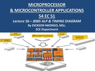
  • 1. MICROPROCESSOR & MICROCONTROLLER APPLICATIONS 54 EC 51 Lecture 5b – 8085 ALP & TIMING DIAGRAM By DICKSON NKONGO, MSc. ECE Department
  • 2. MP & MC APPLICATIONS Lecture 5b – 8085 ALP & Timing Diagram Mr.DicksonNkongo:SJUCET--2017/2018
  • 3. MACHINE CYCLES And Their Timing OF 8085: MP & MC APPLICATIONS Lecture 5 – 8085 ALP & Timing Diagram As far as execution of instructions is concerned, in 8085 microprocessor, each instruction is divided into two parts: 1- The operation code(opcode) and 2 - The operand The opcode tells us what the operation is and the operand is the necessary information required for the instruction. The operand may be either data or an address or other information required for the instruction. Each instruction is divided into machine cycles and each machine cycle is divided into clock cycles or T- states Mr.DicksonNkongo:SJUCET--2017/2018
  • 4. MP & MC APPLICATIONS Lecture 5 – 8085 ALP & Timing Diagram MACHINE CYCLES And Their Timing OF 8085: During normal operation, the microprocessor sequentially fetches, decodes and executes one instruction after another until a halt instruction (HALT). Timing Diagram is the graphical representation of the time taken for the execution of each instruction by a microprocessor. The execution time is represented in T-states. Mr.DicksonNkongo:SJUCET--2017/2018
  • 5. MACHINE CYCLES And Their Timing OF 8085: MP & MC APPLICATIONS Lecture 5 – 8085 ALP & Timing Diagram Instruction Cycle: Is the time required to execute an instruction Machine Cycle: The time required to access the memory or input/output devices is called machine cycle. T-State: The machine cycle and instruction cycle takes multiple clock periods. A portion of an operation carried out in one system clock period is called as T-state. Mr.DicksonNkongo:SJUCET--2017/2018
  • 6. • Clock Signal The 8085 divides the clock frequency provided at X1 and X2 inputs by 2 which is called operating frequency. One T-state is equal to the time period of the internal clock signal of the microprocessor For Ex: If the internal clock frequency of 8085 microprocessor is 3 MHZ, One T-state is equal to • 𝟏 𝒇 = 𝟏 𝟑𝒙𝟏𝟎 𝟔 = 0.333x10⁻⁶sec=333x10-9sec • (333 nano seconds nearly) MP & MC APPLICATIONS Lecture 5 – 8085 ALP & Timing Diagram Mr.DicksonNkongo:SJUCET--2017/2018
  • 7. • Clock Signal T-State 1 Clock cycle Rise time and fall time MP & MC APPLICATIONS Lecture 5 – 8085 ALP & Timing Diagram Mr.DicksonNkongo:SJUCET--2017/2018
  • 8. • Single Signal Single signal status is represented by a line. It may have status either logic 0 or logic 1 or tri-state Logic 0 Logic 1 Tri state MP & MC APPLICATIONS Lecture 5 – 8085 ALP & Timing Diagram Mr.DicksonNkongo:SJUCET--2017/2018
  • 9. • Group of signals Group of signals is also called a bus. Eg: Address bus, data bus State changes Valid state Tri state MP & MC APPLICATIONS Lecture 5 – 8085 ALP & Timing Diagram Mr.DicksonNkongo:SJUCET--2017/2018
  • 10. MP & MC APPLICATIONS Lecture 5 – 8085 ALP & Timing Diagram Mr.DicksonNkongo:SJUCET--2017/2018
  • 11. Machine cycle 2 Machine cycle 5 Instruction cycle T – State 1 T – State 2 T – State 3 T – State 6 MP & MC APPLICATIONS Lecture 5 – 8085 ALP & Timing Diagram Machine cycle 1 Mr.DicksonNkongo:SJUCET--2017/2018
  • 12. The 8085 microprocessor has 5 basic machine cycles. They are 1. Opcode fetch cycle (4T) 2. Memory write cycle (3T) 3. I/O read cycle (3T) 4. Memory read cycle (3T) 5. I/O write cycle (3T) Some more machine cycles for 8085: 1. Interrupt Acknowledge 2. Bus Idle MP & MC APPLICATIONS Lecture 5b – 8085 ALP & Timing Diagram Mr.DicksonNkongo:SJUCET--2017/2018
  • 13. 8085 Machine Cycles The three status signals IO/M*, S1 and S2 identify each type DICKSON NKONGO, MSc. : ECE Department. MP & MC APPLICATIONS Lecture 5b – 8085 ALP & Timing Diagram Mr.DicksonNkongo:SJUCET--2017/2018
  • 14. The Control and Status Signals •There are 4 main control and status signals. These are: • ALE: Address Latch Enable. This signal is a pulse that become 1 when the AD0 – AD7 lines have an address on them. It becomes 0 after that. This signal can be used to enable a latch to save the address bits from the AD lines. • RD’: Read. Active low indicates that the data must be read from the selected memory location or I/O port via data bus. • WR’: Write. Active low indicates that the data must be written into the selected memory location or I/O port via data bus.. • IO/M’: This signal specifies whether the operation is a memory operation (IO/M=0) or an I/O operation (IO/M=1). • S1 and S0: Status signals to specify the kind of operation being performed .Usually un-used in small systems. DICKSON NKONGO, MSc. : ECE Department. MP & MC APPLICATIONS Lecture 5b – 8085 ALP & Timing Diagram Mr.DicksonNkongo:SJUCET--2017/2018
  • 15. Signal Timings ALE  This signal is active high signal. It is activated in the beginning of T1 state of each machine cycle except bus idle machine cycle and it remains active in the T1 state DICKSON NKONGO, MSc. : ECE Department. MP & MC APPLICATIONS Lecture 5b – 8085 ALP & Timing Diagram Mr.DicksonNkongo:SJUCET--2017/2018
  • 16. Signal Timings MP & MC APPLICATIONS Lecture 5b – 8085 ALP & Timing Diagram A0 - A7 (Lower Byte Address) This is available on the multiplexed address/data bus (AD0 - AD7) during T1 state of each machine cycle except bus idle machine cycle. Mr.DicksonNkongo:SJUCET--2017/2018
  • 17. Signal Timings MP & MC APPLICATIONS Lecture 5b – 8085 ALP & Timing Diagram D0 - D7 (Data Bus) The data from memory or I/O device and from microprocessor to memory or I/O device is transferred during T2 and T3 – states. N.B: In read machine cycle, data will appear on the data bus during the later part of the T2 - state as shown in fig. (next slide). This is because to read data from memory or I/O device it is necessary to select memory or I/O device, after the selection, device will put the data from the selected location on the data bus. This action needs finite time. This time is referred as “Access Time”. Mr.DicksonNkongo:SJUCET--2017/2018
  • 18. Signal Timings MP & MC APPLICATIONS Lecture 5b – 8085 ALP & Timing Diagram D0 - D7 (Data Bus) In case of write cycle, data is available in the register set of the microprocessor and it can put that data on the data bus with zero access time. Read Write Mr.DicksonNkongo:SJUCET--2017/2018
  • 19. Signal Timings MP & MC APPLICATIONS Lecture 5b – 8085 ALP & Timing Diagram A8 - A15 (Higher Byte Address)  The higher byte of address is available on the A8 – A15 bus during T1, T2, and T3 – state of each machine cycle, except bus idle machine cycle Mr.DicksonNkongo:SJUCET--2017/2018
  • 20. Signal Timings MP & MC APPLICATIONS Lecture 5b – 8085 ALP & Timing Diagram IO/M*, S0, S1:  These are called status signals. They decide the type of machine cycle to be executed. They are activated at the beginning of T1 – state of each machine cycle and remain active till the end of the machine cycle Mr.DicksonNkongo:SJUCET--2017/2018
  • 21. Signal Timings MP & MC APPLICATIONS Lecture 5b – 8085 ALP & Timing Diagram RD* and WR* (‘*’ here denotes Bar) These decide the direction of the data transfer. When RD* signal is active, data is transmitted from memory or I/O device to microprocessor. When WR* signal is active, data is transmitted from microprocessor to the memory or I/O device. Both signals are never active at a time. **And since the data transfer in 8085 takes place during T2 and T3, these signals are activated during T2 and T3 as shown in the next slide Mr.DicksonNkongo:SJUCET--2017/2018
  • 22. RD* and WR* DICKSON NKONGO, MSc. : ECE Department. MP & MC APPLICATIONS Lecture 5b – 8085 ALP & Timing Diagram Mr.DicksonNkongo:SJUCET--2017/2018
  • 23. • 8085 Machine cycles MP & MC APPLICATIONS Lecture 5b – 8085 ALP & Timing Diagram Mr.DicksonNkongo:SJUCET--2017/2018
  • 24. The Control and Status Signals • (* ) means ‘bar’ i.e. active low IO/M* RD* WR* REMARKS 0 0 1 Reading from memory 0 1 0 Writing into memory 1 0 1 Reading from IO device 1 1 0 Writing into IO device X 1 1 No communication with peripheral DICKSON NKONGO, MSc. : ECE Department. MP & MC APPLICATIONS Lecture 5b – 8085 ALP & Timing Diagram Mr.DicksonNkongo:SJUCET--2017/2018
  • 25. The 8085 microprocessor has 5 basic machine cycles. They are 1. Opcode fetch cycle (4T) 2. Memory write cycle (3T) 3. I/O read cycle (3T) 4. Memory read cycle (3T) 5. I/O write cycle (3T) Some more machine cycles for 8085: 1. Interrupt Acknowledge 2. Bus Idle MP & MC APPLICATIONS Lecture 5b – 8085 ALP & Timing Diagram Mr.DicksonNkongo:SJUCET--2017/2018
  • 26. 1. Opcode Fetch Machine Cycle • The first step of executing any instruction is the Opcode fetch cycle. – In this cycle, the microprocessor brings in the instruction’s Opcode from memory. • To differentiate this machine cycle from the very similar “memory read” cycle, the control & status signals are set as follows: – IO/M’=0, s0 and s1 are both 1. – This machine cycle has four T-states. • The 8085 uses the first 3 T-states to fetch the opcode. • T4 is used to decode and execute it. – It is also possible for an instruction to have 6 T-states in an opcode fetch machine cycle. MP & MC APPLICATIONS Lecture 5b – 8085 ALP & Timing Diagram Mr.DicksonNkongo:SJUCET--2017/2018
  • 27. Machine Cycles MP & MC APPLICATIONS Lecture 5b – 8085 ALP & Timing Diagram 1. Opcode Fetch Machine Cycle: Step 1: (State T1) The 8085 places the contents of PC (Program counter) on the address bus. Higher-order byte of the PC is placed on the A8-A15 lines, while lower- order on AD0-AD7 lines which stays on only during T1. Microprocessor activates ALE which is used to latch the low-order byte of the address before it disappears. 8085 also sends status signals IO/M* = 0, S1=1 and S0 = 1. Mr.DicksonNkongo:SJUCET--2017/2018
  • 28. Machine Cycles MP & MC APPLICATIONS Lecture 5b – 8085 ALP & Timing Diagram 1. Opcode Fetch Machine Cycle: Step 2: (State T2) Lower-byte address disappears from the AD0- AD7 lines. However A0-A7 remain available as they were latched during T1. 8085 sends RD* signal low to enable the addressed memory location. Then memory device places the contents of the addressed memory location on the data bus (AD0-AD7). Mr.DicksonNkongo:SJUCET--2017/2018
  • 29. Machine Cycles MP & MC APPLICATIONS Lecture 5b – 8085 ALP & Timing Diagram 1. Opcode Fetch Machine Cycle: Step 3: (State T3) 8085 loads the data (opcode in this case) from the data bus in its Instruction register. Then raises RD* to high which disables the memory device (deactivate RD signal) Mr.DicksonNkongo:SJUCET--2017/2018
  • 30. Machine Cycles MP & MC APPLICATIONS Lecture 5b – 8085 ALP & Timing Diagram 1. Opcode Fetch Machine Cycle: Step 4: (State T4) Microprocessor decodes the opcode, and on the basis of the instruction received, it decides whether to enter state T5 or to enter state T1 of the next machine cycle. One byte instructions which operates on eight bit data (8 bit operand) are executed in T4. (e.g. MOV A, B, ANA D, ADD C). This is because for one byte instructions which operate on eight bit data, data is always available in the internal memory of 8085 i.e. registers Mr.DicksonNkongo:SJUCET--2017/2018
  • 31. Machine Cycles MP & MC APPLICATIONS Lecture 5b – 8085 ALP & Timing Diagram 1. Opcode Fetch Machine Cycle: Step 5: (State T5 and T6) Used for internal microprocessor operations required by the instruction. One byte instructions which operates on sixteen bit data (16 bit operand) are executed in T5 and T6. (e.g. DCX H, PCHL, SPHL, INX H etc. Mr.DicksonNkongo:SJUCET--2017/2018
  • 32. Timing Diagram for Opcode Fetch Machine Cycle MP & MC APPLICATIONS Lecture 5 – 8085 ALP & Timing Diagram Mr.DicksonNkongo:SJUCET--2017/2018
  • 33. Timing Diagram for Opcode Fetch Machine Cycle MP & MC APPLICATIONS Lecture 5 – 8085 ALP & Timing Diagram
  • 34. Timing Diagram for Opcode Fetch Machine Cycle State T1 IO/M*=0, S1=1, S0=1 State T2 . . RD* = 0 Data State T3 RD* = 1 State T4 Opcode Decoded
  • 35. (b)Timing Diagram for Opcode Fetch Machine Cycle MP & MC APPLICATIONS Lecture 5 – 8085 ALP & Timing Diagram
  • 36. Machine Cycles MP & MC APPLICATIONS Lecture 5b – 8085 ALP & Timing Diagram 2. Memory Read Cycle:  8085 executes this cycle to read the contents of R/W memory (RAM) or ROM.  The length of this machine cycle is 3-T states (T1- T3). Step 1: (State T1) Microprocessor places the address on the address lines from stack pointer, general purpose register pair or program counter and then activates the ALE signal for latching the low-byte of address. Also microprocessor sends status signals: IO/M* = 0, S1 = 1, and S0 = 0 (for memory read machine cycle) Mr.DicksonNkongo:SJUCET--2017/2018
  • 37. Machine Cycles MP & MC APPLICATIONS Lecture 5b – 8085 ALP & Timing Diagram 2. Memory Read Cycle: Step 2: (State T2) Microprocessor sends RD* signal low to enable addressed memory location. Then memory device places the contents of the addressed memory location on the data bus (AD0- AD7) Step 3: (State T3) 8085 loads the data from the data bus into specified register (A, B, C, D, E, H, H, and L) and raises RD* to high which disables the memory device Mr.DicksonNkongo:SJUCET--2017/2018
  • 38. Machine Cycles MP & MC APPLICATIONS Lecture 5 – 8085 ALP & Timing Diagram 2. Memory Read Cycle: .
  • 39. Machine Cycles MP & MC APPLICATIONS Lecture 5 – 8085 ALP & Timing Diagram 2. Memory Read Cycle: . Mr.DicksonNkongo:SJUCET--2017/2018
  • 40. State T1 IO/M*=0, S1=1, S0=0 State T2 . . RD* = 0 Data State T3 RD* = 1
  • 41. Timing Diagram for Memory Read Machine Cycle MP & MC APPLICATIONS Lecture 5b – 8085 ALP & Timing Diagram Mr.DicksonNkongo:SJUCET--2017/2018
  • 42. Machine Cycles MP & MC APPLICATIONS Lecture 5 – 8085 ALP & Timing Diagram 2. Memory Read Cycle: .
  • 43. Timing diagram for MVI A, 30H instruction – To understand the memory read machine cycle, let’s study the execution of the following instruction: • MVI A, 30 – In memory, this instruction looks like: • The first byte 3EH represents the opcode for loading a byte into the accumulator (MVI A), the second byte is the data to be loaded. 2000H 2001H 3E 30 MP & MC APPLICATIONS Lecture 5b – 8085 ALP & Timing Diagram Mr.DicksonNkongo:SJUCET--2017/2018
  • 44. Timing diagram for MVI A, 30H instruction The 8085 needs to read these two bytes from memory before it can execute the instruction. Therefore, it will need at least two machine cycles. 1. The first machine cycle is the opcode fetch discussed earlier. 2. The second machine cycle is the Memory Read Cycle. 2000H 2001H 3E 30 MP & MC APPLICATIONS Lecture 5b – 8085 ALP & Timing Diagram Mr.DicksonNkongo:SJUCET--2017/2018
  • 45. Timing diagram for MVI A, 30H instruction Mr.DicksonNkongo:SJUCET--2017/2018
  • 46. Machine Cycles MP & MC APPLICATIONS Lecture 5b – 8085 ALP & Timing Diagram 3. Memory Write Cycle: 8085 executes this cycle to store the data into data memory or stack. The length of this machine cycle is 3-T states (T1- T3). Step 1: (State T1) Microprocessor places the address on the address lines from stack pointer, general purpose register pair and then activates the ALE signal for latching the low-byte of address. Also microprocessor sends status signals: IO/M* = 0, S1 = 0, and S0 = 1 (for memory write machine cycle) Mr.DicksonNkongo:SJUCET--2017/2018
  • 47. Machine Cycles MP & MC APPLICATIONS Lecture 5b – 8085 ALP & Timing Diagram 3. Memory Write Cycle: Step 2: (State T2) Microprocessor places the data on the data bus and sends WR* signal low for writing into the addressed memory location. Step 3: (State T3) 8085 writes (stores) the data from the data bus into addressed memory location and raises WR* to high which disables the memory device and terminates the write operation. Mr.DicksonNkongo:SJUCET--2017/2018
  • 48. Memory Write Data Flow MP & MC APPLICATIONS Lecture 5 – 8085 ALP & Timing Diagram
  • 49. Memory Write Data Flow MP & MC APPLICATIONS Lecture 5 – 8085 ALP & Timing Diagram Mr.DicksonNkongo:SJUCET--2017/2018
  • 50. State T1 IO/M*=0, S1=0, S0=1 State T2 . . WR* = 0 DataState T3 WR* = 1 Data
  • 51. Timing Diagram for Memory Write Machine Cycle Mr.DicksonNkongo:SJUCET--2017/2018
  • 52. The I/O Read and I/O Write Operation • the I/O read and I/O write machine cycles are similar to the memory read and memory write machine cycles respectively, except that IO/M* signal is High (1) for I/O read and I/O write machine cycles. • High IO/M* indicates that it is an I/O operation. MP & MC APPLICATIONS Lecture 5b – 8085 ALP & Timing Diagram Mr.DicksonNkongo:SJUCET--2017/2018
  • 53. Machine Cycles MP & MC APPLICATIONS Lecture 5b – 8085 ALP & Timing Diagram 4. I/O Read Cycle: 8085 executes this cycle to read the data from I/O device. The length of this machine cycle is 3-T states (T1- T3). Step 1: (State T1) Microprocessor places the address on the address lines from stack pointer, general purpose register pair or program counter and then activates the ALE signal for latching the low-byte of address. Also microprocessor sends status signals: IO/M* = 1, S1 = 1, and S0 = 0 (for I/O read machine cycle) Mr.DicksonNkongo:SJUCET--2017/2018
  • 54. Machine Cycles MP & MC APPLICATIONS Lecture 5b – 8085 ALP & Timing Diagram 4. I/O Read Cycle: Step 2: (State T2) Microprocessor sends RD* signal low to enable addressed memory location. Then I/O device places data on the data bus (AD0-AD7) Step 3: (State T3) 8085 loads the data from the data bus into specified register (A, B, C, D, E, H, H, and L) and raises RD* to high which disables the I/O device Mr.DicksonNkongo:SJUCET--2017/2018
  • 55. Machine Cycles MP & MC APPLICATIONS Lecture 5 – 8085 ALP & Timing Diagram 4. I/O Read Cycle: .
  • 56. Machine Cycles MP & MC APPLICATIONS Lecture 5 – 8085 ALP & Timing Diagram 4. I/O Read Cycle: .
  • 57. Machine Cycles 4. I/O Read Cycle: . Timing Diagram for I/O Read Machine Cycle Mr.DicksonNkongo:SJUCET--2017/2018
  • 58. Machine Cycles MP & MC APPLICATIONS Lecture 5b – 8085 ALP & Timing Diagram 5. I/O Write Cycle: 8085 executes this cycle to store the data into data IO device. The length of this machine cycle is 3-T states (T1- T3). Step 1: (State T1) Microprocessor places the address on the address lines from stack pointer, general purpose register pair and then activates the ALE signal for latching the low-byte of address. Also microprocessor sends status signals: IO/M* = 1, S1 = 0, and S0 = 1 (for I/O write machine cycle) Mr.DicksonNkongo:SJUCET--2017/2018
  • 59. Machine Cycles MP & MC APPLICATIONS Lecture 5b – 8085 ALP & Timing Diagram 5. I/O Write Cycle: Step 2: (State T2) Microprocessor places the data on the data bus and sends WR* signal low for writing into the addressed I/O device. Step 3: (State T3) 8085 writes (stores) the data from the data bus into addressed I/O device and raises WR* to high which disables the I/O device and terminates the write operation. Mr.DicksonNkongo:SJUCET--2017/2018
  • 60. MP & MC APPLICATIONS Lecture 5 – 8085 ALP & Timing Diagram
  • 61.
  • 62. Timing Diagram for I/O Write Machine Cycle Mr.DicksonNkongo:SJUCET--2017/2018

Editor's Notes

  1. Opcode fetch cycle (4T) Memory write cycle (3T) I/O read cycle (3T) Memory read cycle (3T) I/O write cycle (3T)
  2. Opcode fetch cycle (4T) Memory write cycle (3T) I/O read cycle (3T) Memory read cycle (3T) I/O write cycle (3T)
  3. Opcode fetch cycle (4T) Memory write cycle (3T) I/O read cycle (3T) Memory read cycle (3T) I/O write cycle (3T)
  4. can process 8-bit at a time. Instructions
  5. Tri-state – represented by dotted lines
  6. Tri-state – represented by dotted lines
  7. Tri-state – represented by dotted lines: Red – Address/Data, Green - Signal ctrl + arrows – small movement Alt + arrow – rotation; shift + arrow = Enlarging the size
  8. Tri-state – represented by dotted lines
  9. can process 8-bit at a time. Instructions
  10. can process 8-bit at a time. Instructions
  11. can process 8-bit at a time. Instructions
  12. can process 8-bit at a time. Instructions
  13. Tri-state – represented by dotted lines: Red – Address/Data, Green - Signal ctrl + arrows – small movement Alt + arrow – rotation; shift + arrow = Enlarging the size
  14. can process 8-bit at a time. Instructions
  15. can process 8-bit at a time. Instructions
  16. can process 8-bit at a time. Instructions
  17. Tri-state – represented by dotted lines: Red – Address/Data, Green - Signal ctrl + arrows – small movement Alt + arrow – rotation; shift + arrow = Enlarging the size
  18. Asserts-Causes others to recognize one’s right
  19. can process 8-bit at a time. Instructions
  20. can process 8-bit at a time. Instructions
  21. can process 8-bit at a time. Instructions
  22. can process 8-bit at a time. Instructions
  23. can process 8-bit at a time. Instructions
  24. can process 8-bit at a time. Instructions
  25. can process 8-bit at a time. Instructions
  26. Asserts-Causes others to recognize one’s right
  27. Asserts-Causes others to recognize one’s right
  28. Asserts-Causes others to recognize one’s right