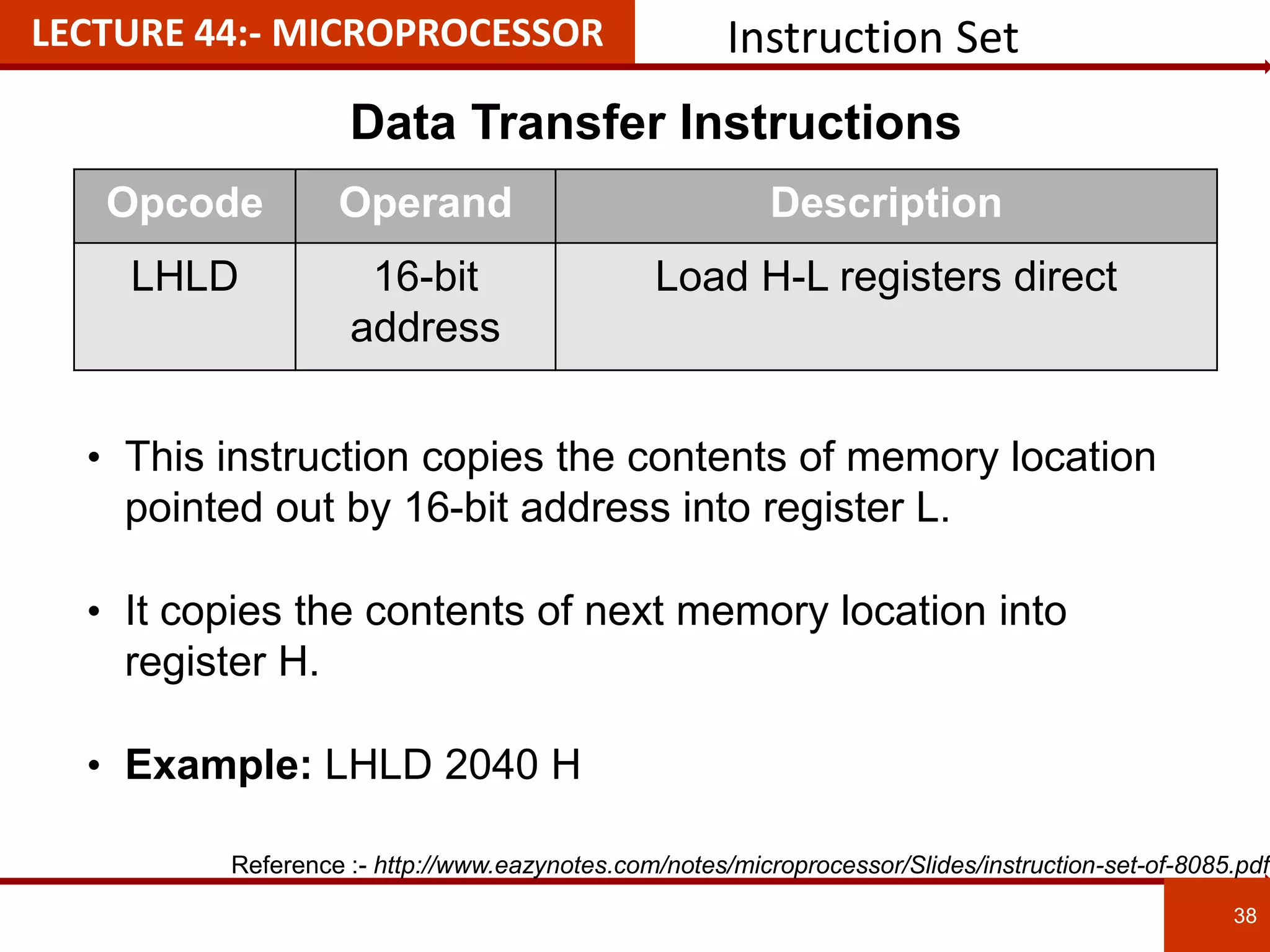
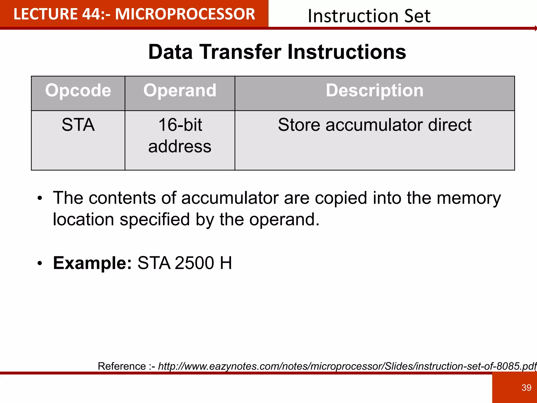
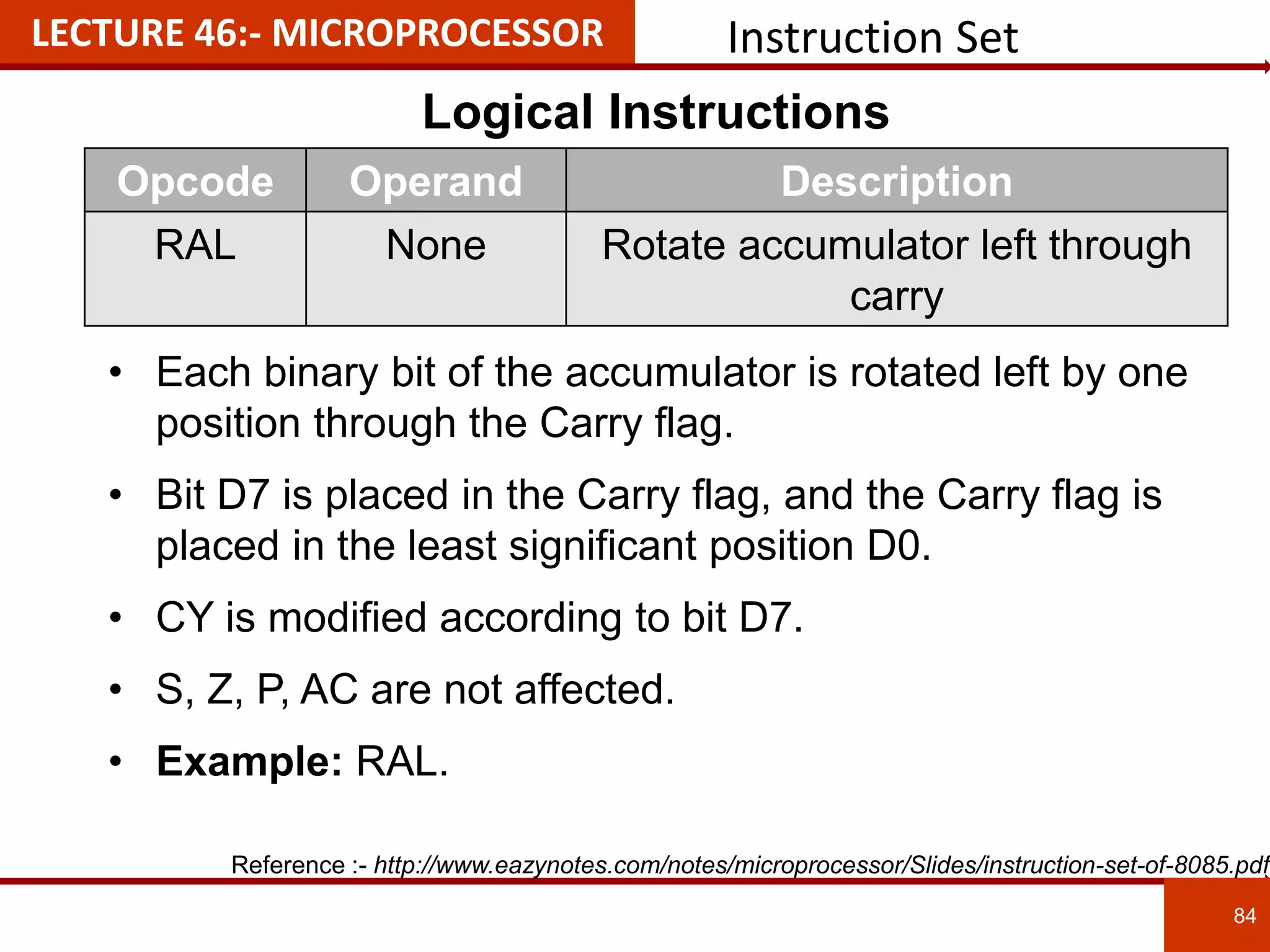
SlideShare a Scribd company logo
1 of 199
Download to read offline
1
DEPARTMENT OF INFORMATION TECHNOLOGY &
ELECTRONICS ENGINEERING
“DIGITAL ELECTRONICS AND
FUNDAMENTAL OF MICROPROCESSOR - II”
(COPYRIGHT REGISTRATION NO. L-71129/2017)
DATTA MEGHE INSTITUTE OF MEDICAL SCIENCE’S
DATTA MEGHE INSTITUTE OF ENGINEERING, TECHNOLOGY & RESEARCH,
SAWANGI(MEGHE), WARDHA. 442001(MS)
AUTHOR
MR. PRAVIN W. JARONDE
Presentation of Notes on
2
Copyright Certificate
PREFACE
As educators, we all have the same common goal “to guide our students” so that they
gain the maximum possible in a positive environment that promotes their success
and inculcates in them desire to learn. One of the best tools available to us in this
pursuit is PPT instruction that is systematic and self Learning. The goal of this PPT
is to help teachers in the use of eLearning that it is both
effective and efficient method for teaching our students. It has been developed for
purely academic and non-commercial purpose.
My desire in preparing this PPT is to support the teachers, who have the very
demanding task of Teaching-Plan to deliver instruction on a lecture/period basis.
The PPT is therefore prepared lecture wise. Further at the end of each chapter
summary and also questions for practice has been provided on the same chapter.
In Chapter 5 we concentrate on basics of 8085 Microprocessor. Chapter 6 presents
Understanding of interrupts, timing diagram and programming of 8085.
With deep regards and humility, I thank my Management of MGI for motivating and our
CEO for strong follow-ups to prepare PPTs under DTEL also Dr. Ashwin Kothari,
Associate Professor, VNIT, Nagpur for his valuable suggestions. I dedicate this PPT to
my dear students and my shared profession.
For any suggestions write me at :- pravinwj@rediffmail.com
3Pravin Jaronde
CONTENT: DIGITAL CIRCUIT & FUNDAMENTAL OF MICROPROCESSOR
4
CHAPTER 5:5
CHAPTER 6:6 Interrupt of 8085
Basic of 8085
Slide No:6
Slide No:135
GENERAL OBJECTIVE
5
The student will be able to:
5
Understand the Architecture, Addressing modes and
Instruction set of 8085 Microprocessor.
6
Write ALP of 8085 Microprocessor also know the
importance of Interrupt.
6
“DIGITAL ELECTRONICS AND
FUNDAMENTAL OF MICROPROCESSOR”
CHAPTER – 5
“BASIC OF 8085 MICROPROCESSOR”
CHAPTER 5:- Basic of 8085 Microprocessor
Introduction to 8085 Microprocessor1
Architecture of 80852
Instruction Sets4
7
Addressing Modes3
Topic 1:
Topic 2:
Topic 3:
Topic 4:
CHAPTER-5 SPECIFIC OBJECTIVE / COURSE OUTCOME
Outline the functional block diagram of Intel 8085 Microprocessor1
List the feature of 8085 Microprocessor2
8
The student will be able to:
Understand Addressing Modes of 8085 Microprocessor3
Program by using different Instructions of 8085 Microprocessor4
9
9
LECTURE 38:- MICROPROCESSOR Introduction to Microprocessor
• Microprocessor is an integrated circuit that contains all the
functions of a central processing unit of a computer.
• Computer having basically four parts – Microprocessor as
CPU, Memory, Input Device and Output Device.
• Microprocessor is the Brain of the computer.
• Here processing, controlling and decision making is done.
Microprocessor
as CPU
Output
Device
Input
Device
Memory
Input Output
Fig 5.1 :Block diagram of Computer
Introduction
10
10
• It is a 8 bit(as data bus is 8-bit) & 40 pin Microprocessor.
• It is a single chip NMOS device.
• It requires a single +5v power suply.
• It provides on chip clock generator.
• The maximum clock frequency is 3 MHz and the
minimum clock frequency is 500Hz.
• It provides 74 instructions with following addressing
modes – register, direct, immediate, indirect and implied.
• Lower byte address bus multiplexed with data bus.
• It provides 16 address lines.
• It provides 5 hardware interrupts: TRAP, RST 5.5, RST
6.5, RST 7.5, INTR.
LECTURE 38:- MICROPROCESSOR
Salient Feature of 8085 Microprocessor
Introduction to Microprocessor
Architecture of 8085
11
LECTURE 39:- MICROPROCESSOR
Reference :- fac-web.spsu.edu/ecet/apreethy/2210_resources/8085.pptFig.5.2 :Architecture of 8085
12
12
• The architecture is divided in different groups as follows-
– Arithmetic and Logical group
– Register group
– Interrupt control group
– Serial I/O control group
– Instruction register, decoder, timing and control group
• Arithmetic group consists of ALU, accumulator,
temporary register and flag register.
• Register group consists of Temporary register, General
purpose register, Special purpose register.
• Interrupt Control group accepts input such as TRAP,
RST 5.5, RST 6.5, RST 7.5, INTR.
LECTURE 39:- MICROPROCESSOR
Architecture of 8085 Microprocessor
Architecture of 8085
13
13
• Serial I/O control group: Data transfer on D0 to D7 lines
is a parallel data, but under certain condition it is
advantageous to use serial data transfer. 8085
implement this by using SID and SOD signals and to
perform serial data transfer there are two special
instructions RIM and SIM.
• Instruction register, Decoder, Timing & Control group :
Instruction fetched from memory is loaded in Instruction
register. These content are then provided to decoder for
decoding. Control section accept information from
instruction decoder generates microsteps to perform it.
By using clock input it perform sequencing and
synchronizing operations.
LECTURE 39:- MICROPROCESSOR
Architecture of 8085 Microprocessor
Architecture of 8085
14
Pin Diagram of 8085LECTURE 40:- MICROPROCESSOR
Reference :- whathub.blogspot.comFig.5.3 :Pin Diagram of 8085
15
Demultiplexing
15
15
Demultiplexing the address/ databus
LECTURE 40:- MICROPROCESSOR
• As lower byte of address and data bus are multiplexed,
external hardware 74LS373 is required to separate it.
Reference :- www.slideshare.net/shashank03/8085-architecture-memory-interfacing1
Fig.5.4 :Demultiplexing
16
• The 8085 is an 8-bit general purpose microprocessor that can
address 64K Byte of memory.
• It has 40 pins and uses +5V for power. It can run at a
maximum frequency of 3 MHz.
– The pins on the chip can be grouped into 6 groups:
❖Address Bus.
❖Data Bus.
❖Control and Status Signals.
❖Power supply and frequency.
❖Externally Initiated Signals.
❖Serial I/O ports.
Various Buses & SignalsLECTURE 41:- MICROPROCESSOR
Buses and Signals in 8085
Control and Status Signals
17
17
• There are 5 main control and status signals. These are:
– Address Latch Enable (ALE)
– Read (RD)’
– Wrire (WR)’
– Input Output / Memory (IO/(M)’)
– Status Signal (S0 and S1)
➢ Address Latch Enable (ALE):
It is a output signal with positive going pulse. Used to
separate AD0-AD7. When pulse is HIGH the content of
AD0-AD7 is address, when it is LOW the content is data.
➢ Read (RD)’: It is a active low, output control signal used
to read (fetch) data from memory or I/O devices.
LECTURE 41:- MICROPROCESSOR Various Buses & Signals
18
18
➢ Write (WR)’: It is a active low, output control signal used to
write data to memory or I/O devices.
➢ Input Output / Memory (IO/M’): This is a output status
signal used to give information of operation to be
performed by microprocessor with memory or I/O device.
When IO/M’=0 it performing memory related operation,
when IO/M’=1 it performing I/O device related operation.
➢ Status Signal (S0 & S1): These are output status signal
used to give information of opertaion performed by
microprocessor. Different four cycles are as follows-
a) OPCODE fetch(Instruction read from mem.) S0=1,S1=1
b) Read (Data read from mem.) S0=0, S1=1
c) Write S0=1, S1=0; d) Halt S0=0, S1=0.
LECTURE 41:- MICROPROCESSOR
Control and Status Signals
Various Buses & Signals
Frequency Control Signals
19
19
• There are 3 important pins in the frequency control
group.
➢ X0 and X1 are the inputs from the crystal or clock
generating circuit.The frequency is internally divided
by 2. So, to run the microprocessor at 3 MHz, a clock
running at 6 MHz should be connected to the X0 and
X1 pins.
➢ CLK (OUT): An output clock pin to drive the clock of
the rest of the system.
LECTURE 41:- MICROPROCESSOR Various Buses & Signals
Generating Control Signals
20
20
• The 8085 generates a single RD’ signal. However, the
signal needs to be used with both memory and I/O. So, it
must be combined with the IO/M’ signal to generate
different control signals for the memory and I/O.
– Keeping in mind the operation of the IO/M’ signal we
can use the following circuitry to generate the right set
of signals:
LECTURE 42:- MICROPROCESSOR Various Buses & Signals
Reference :- www.indiastudychannel.com/attachments/.../101798-9259-8085.ppt
Fig.5.5 :Control Signals
21
Various Registers of 8085
21
21
LECTURE 42:- MICROPROCESSOR
Register Block of 8085
• It provides one accumulator, one flag register, 6 general
purpose register and two special purpose registers.
• General purpose register – B,C,D,E,H and L
• Special purpose register – Stack pointer and Program
counter.
Fig.5.6:Register Block of 8085
22
22
• Register pairs: 8 bit registers can also be combined as
register pairs to perform 16-bit operations: BC, DE, HL.
• Accumulator:
-Single 8-bit register that is part of the ALU.
-Used for arithmetic / logic operations – the result is
always stored in the accumulator.
• Program Counter (PC): Contains the memory address
(16 bits) of the instruction that will be executed in the next
steps.
• Stack pointer (SP): A register that holds the address of
the top item in the stack. SP always points at the top item
in the stack.
LECTURE 42:- MICROPROCESSOR Various Registers of 8085
Registers of 8085
Flag Register of 8085
23
23
LECTURE 42:- MICROPROCESSOR Various Registers of 8085
• The flag register in 8085 is an 8-bit register
• Out of 8 bit only 5 bit are in use.
• These five flags are of 1bit Flip Flop and are as follows-
a) Sign flag (S)
b) Zero flag (Z)
c) Auxiliary Carry flag (AC)
d) Parity flag (P)
e) Carry flag (CY)
Fig. 5.7 :Structure of Flag register
Flag Register of 8085
24
24
LECTURE 42:- MICROPROCESSOR Various Registers of 8085
The Flag register are gets affected only on the result of the
ALU. As per operation performed by ALU flag register gets
updated as below-
• Sign flag is set if the most significant bit of the ALU result
is set.
• Zero flag is set if the result of ALU (instruction) is zero.
• Auxiliary carry flag is set if there is a carry out from bit 3
to bit 4 of the ALU result.
• Parity flag is set if the parity ( the number of set bits in the
result is even.
• Carry flag is set if there is a carry during addition, or
borrow during subtraction/ comparison.
LECTURE 43:- MICROPROCESSOR Addressing Modes
25
25
Types Of Addressing Mode
• Every instruction of a program has to operate on a data.
• The method of specifying the data to be operated by the
instruction is called Addressing.
• The 8085 has the following 5 different types of
addressing(Operation wise).
1. Immediate Addressing
2. Direct Addressing
3. Register Direct Addressing
4. Register Indirect Addressing
5. Implied/Implicit Addressing
LECTURE 43:- MICROPROCESSOR Addressing Modes
26
26
Immediate Addressing
• In immediate addressing mode, the data is specified in
the instruction itself. The data will be a part of the
program instruction.
Example:
• MVI B, 3EH – Move the data 3EH given in the instruction
to B register;
• LXI SP, 2700H – Move the data 2700h to stack pointer.
LECTURE 43:- MICROPROCESSOR Addressing Modes
27
27
Direct Addressing
• In direct addressing mode, the address of the data is
specified in the instruction. The data will be in memory.
In this addressing mode, the program instructions and
data can be stored in different memory.
Example:
• LDA 1050H - Load the data available in memory location
1050H in to accumulator;
• SHLD 3000H - The content of location 3000H is copied
into the HL register pair.
LECTURE 43:- MICROPROCESSOR Addressing Modes
28
28
Register Direct Addressing
• In register addressing mode, the instruction specifies the
name of the register in which the data is available.
Example:
• MOV A, B - Move the content of B register to A register;
• SPHL - Copy H-L pair to the Stack Pointer (SP)
• ADD C - Add register C with Accumulator.
LECTURE 43:- MICROPROCESSOR Addressing Modes
29
29
Register Indirect Addressing
• In register indirect addressing mode, the instruction
specifies the name of the register in which the address of
the data is available. Here the data will be in memory
and the address will be in the register pair.
Example:
• MOV A, M - The memory data addressed by H L pair is
moved to A register.
• LDAX B - loads the accumulator with the contents of a
memory location addressed by B, C register pair.
LECTURE 43:- MICROPROCESSOR Addressing Modes
30
30
Implied Addressing
• In implied addressing mode, the instruction itself
specifies the data to be operated.
Example:
• CMA - Complement the content of accumulator;
• RAL - Rotate accumulator left through carry.
LECTURE 44:- MICROPROCESSOR Instruction Set
31
31
Instruction Set of 8085
• An instruction is a binary pattern designed inside a
microprocessor to perform a specific function.
• The entire group of instructions that a microprocessor
supports is called Instruction Set.
• 8085 has 246 instructions.
• Each instruction is represented by an 8-bit binary value.
• These 8-bits of binary value is called Op-Code or
Instruction Byte.
Reference :- http://www.eazynotes.com/notes/microprocessor/Slides/instruction-set-of-8085.pdf
LECTURE 44:- MICROPROCESSOR Instruction Set
32
32
Classification of Instruction Set
• Data Transfer Instruction
• Arithmetic Instructions
• Logical Instructions
• Branching Instructions
• Stack and Machine Control Instructions
Reference :- http://www.eazynotes.com/notes/microprocessor/Slides/instruction-set-of-8085.pdf
LECTURE 44:- MICROPROCESSOR Instruction Set
33
33
Data Transfer Instructions
• These instructions move data between registers, or
between memory and registers.
• These instructions copy data from source to destination.
• While copying, the contents of source are not modified.
• This operation doesn’t affect flag.
Reference :- http://www.eazynotes.com/notes/microprocessor/Slides/instruction-set-of-8085.pdf
LECTURE 44:- MICROPROCESSOR
34
34
Data Transfer Instructions
• This instruction copies the contents of the source
register into the destination register.
• The contents of the source register are not altered.
• If one of the operands is a memory location, its location
is specified by the contents of the HL registers.
• Example: MOV B, C or MOV B, M
Opcode Operand Description
MOV Rd, Rs
M, Rs
Rd, M
Copy from source to destination.
Instruction Set
Reference :- http://www.eazynotes.com/notes/microprocessor/Slides/instruction-set-of-8085.pdf
LECTURE 44:- MICROPROCESSOR
35
35
Data Transfer Instructions
• The 8-bit data is stored in the destination register or
memory.
• If the operand is a memory location, its location is
specified by the contents of the H-L registers.
• Example: MVI B, 57H or MVI M, 57H
Opcode Operand Description
MVI Rd, Data
M, Data
Move immediate 8-bit
Instruction Set
Reference :- http://www.eazynotes.com/notes/microprocessor/Slides/instruction-set-of-8085.pdf
LECTURE 44:- MICROPROCESSOR
36
36
Data Transfer Instructions
• The contents of the designated register pair point to a
memory location.
• This instruction copies the contents of that memory
location into the accumulator.
• The contents of either the register pair or the memory
location are not altered. Example: LDAX B
Opcode Operand Description
LDAX B/D
Register
Pair
Load accumulator indirect
Instruction Set
Reference :- http://www.eazynotes.com/notes/microprocessor/Slides/instruction-set-of-8085.pdf
LECTURE 44:- MICROPROCESSOR
37
37
Data Transfer Instructions
• This instruction loads 16-bit data in the register pair.
• Example: LXI H, 2034 H
Opcode Operand Description
LXI Reg. pair,
16-bit data
Load register pair immediate
Instruction Set
Reference :- http://www.eazynotes.com/notes/microprocessor/Slides/instruction-set-of-8085.pdf
LECTURE 44:- MICROPROCESSOR
38
38
Data Transfer Instructions
• This instruction copies the contents of memory location
pointed out by 16-bit address into register L.
• It copies the contents of next memory location into
register H.
• Example: LHLD 2040 H
Opcode Operand Description
LHLD 16-bit
address
Load H-L registers direct
Instruction Set
Reference :- http://www.eazynotes.com/notes/microprocessor/Slides/instruction-set-of-8085.pdf
LECTURE 44:- MICROPROCESSOR
39
39
Data Transfer Instructions
• The contents of accumulator are copied into the memory
location specified by the operand.
• Example: STA 2500 H
Opcode Operand Description
STA 16-bit
address
Store accumulator direct
Instruction Set
Reference :- http://www.eazynotes.com/notes/microprocessor/Slides/instruction-set-of-8085.pdf
LECTURE 44:- MICROPROCESSOR
40
40
Data Transfer Instructions
• The contents of accumulator are copied into the memory
location specified by the contents of the register pair.
• Example: STAX B
Opcode Operand Description
STAX Reg. pair Store accumulator indirect
Instruction Set
Reference :- http://www.eazynotes.com/notes/microprocessor/Slides/instruction-set-of-8085.pdf
LECTURE 44:- MICROPROCESSOR
41
41
Data Transfer Instructions
• The contents of register L are stored into memory
location specified by the 16-bit address.
• The contents of register H are stored into the next
memory location.
• Example: SHLD 2550 H
Opcode Operand Description
SHLD 16-bit
address
Store H-L registers direct
Instruction Set
Reference :- http://www.eazynotes.com/notes/microprocessor/Slides/instruction-set-of-8085.pdf
LECTURE 44:- MICROPROCESSOR
42
42
Data Transfer Instructions
• The contents of register H are exchanged with the
contents of register D.
• The contents of register L are exchanged with the
contents of register E.
• Example: XCHG
Opcode Operand Description
XCHG None Exchange H-L with D-E
Instruction Set
Reference :- http://www.eazynotes.com/notes/microprocessor/Slides/instruction-set-of-8085.pdf
LECTURE 44:- MICROPROCESSOR
43
43
Data Transfer Instructions
• This instruction loads the contents of H-L pair into SP.
• Example: SPHL
Opcode Operand Description
SPHL None Copy H-L pair to the Stack
Pointer (SP)
Instruction Set
Reference :- http://www.eazynotes.com/notes/microprocessor/Slides/instruction-set-of-8085.pdf
LECTURE 44:- MICROPROCESSOR
44
44
Data Transfer Instructions
• The contents of L register are exchanged with the
location pointed out by the contents of the SP.
• The contents of H register are exchanged with the next
location (SP + 1).
• Example: XTHL
Opcode Operand Description
XTHL None Exchange H–L with top of stack
Instruction Set
Reference :- http://www.eazynotes.com/notes/microprocessor/Slides/instruction-set-of-8085.pdf
LECTURE 44:- MICROPROCESSOR
45
45
Data Transfer Instructions
• The contents of registers H and L are copied into the
program counter (PC).
• The contents of H are placed as the high-order byte and
the contents of L as the low-order byte.
• Example: PCHL
Opcode Operand Description
PCHL None Load program counter with H-L
contents
Instruction Set
Reference :- http://www.eazynotes.com/notes/microprocessor/Slides/instruction-set-of-8085.pdf
LECTURE 44:- MICROPROCESSOR
46
46
Data Transfer Instructions
• The contents of register pair are copied onto stack.
• SP is decremented and the contents of high-order
registers (B, D, H, A) are copied into stack.
• SP is again decremented and the contents of low-order
registers (C, E, L, Flags) are copied into stack.
• Example: PUSH B
Opcode Operand Description
PUSH Reg. pair Push register pair onto stack
Instruction Set
Reference :- http://www.eazynotes.com/notes/microprocessor/Slides/instruction-set-of-8085.pdf
LECTURE 44:- MICROPROCESSOR
47
47
Data Transfer Instructions
• The contents of top of stack are copied into register pair.
• The contents of location pointed out by SP are copied to
the low-order register (C, E, L, Flags).
• SP is incremented and the contents of location are
copied to the high-order register (B, D, H, A).
• Example: POP H
Opcode Operand Description
POP Reg. pair Pop stack to register pair
Instruction Set
Reference :- http://www.eazynotes.com/notes/microprocessor/Slides/instruction-set-of-8085.pdf
LECTURE 44:- MICROPROCESSOR
48
48
Data Transfer Instructions
• The contents of accumulator are copied into the I/O port.
• Example: OUT 78 H
Opcode Operand Description
OUT 8-bit port
address
Copy data from accumulator to a
port with 8-bit address
Instruction Set
Reference :- http://www.eazynotes.com/notes/microprocessor/Slides/instruction-set-of-8085.pdf
LECTURE 44:- MICROPROCESSOR
49
49
Data Transfer Instructions
• The contents of I/O port are copied into accumulator.
• Example: IN 8C H
Opcode Operand Description
IN 8-bit port
address
Copy data to accumulator from a
port with 8-bit address
Instruction Set
Reference :- http://www.eazynotes.com/notes/microprocessor/Slides/instruction-set-of-8085.pdf
LECTURE 45:- MICROPROCESSOR
50
50
Arithmetic Instructions
• These instructions perform the operations like:
– Addition
– Subtract
– Increment
– Decrement
Instruction Set
Reference :- http://www.eazynotes.com/notes/microprocessor/Slides/instruction-set-of-8085.pdf
LECTURE 45:- MICROPROCESSOR
51
51
Addition
• Any 8-bit number, or the contents of register, or the
contents of memory location can be added to the
contents of accumulator.
• The result (sum) is stored in the accumulator.
• No two other 8-bit registers can be added directly.
• Example: The contents of register B cannot be added
directly to the contents of register C.
Instruction Set
Reference :- http://www.eazynotes.com/notes/microprocessor/Slides/instruction-set-of-8085.pdf
LECTURE 45:- MICROPROCESSOR
52
52
Subtraction
• Any 8-bit number, or the contents of register, or the
contents of memory location can be subtracted from the
contents of accumulator.
• The result is stored in the accumulator.
• Subtraction is performed in 2’s complement form.
• If the result is negative, it is stored in 2’s complement
form.
• No two other 8-bit registers can be subtracted directly.
Instruction Set
Reference :- http://www.eazynotes.com/notes/microprocessor/Slides/instruction-set-of-8085.pdf
LECTURE 45:- MICROPROCESSOR
53
53
Increment / Decrement
• The 8-bit contents of a register or a memory location can
be incremented or decremented by 1.
• The 16-bit contents of a register pair can be incremented
or decremented by 1.
• Increment or decrement can be performed on any
register or a memory location.
Instruction Set
Reference :- http://www.eazynotes.com/notes/microprocessor/Slides/instruction-set-of-8085.pdf
LECTURE 45:- MICROPROCESSOR
54
54
Arithmetic Instructions
• The contents of register or memory are added to the
contents of accumulator.
• The result is stored in accumulator.
• If the operand is memory location, its address is
specified by H-L pair.
• All flags are modified to reflect the result of the addition.
• Example: ADD B or ADD M
Opcode Operand Description
ADD R
M
Add register or memory to
accumulator
Instruction Set
Reference :- http://www.eazynotes.com/notes/microprocessor/Slides/instruction-set-of-8085.pdf
LECTURE 45:- MICROPROCESSOR
55
55
Arithmetic Instructions
• The contents of register or memory and Carry Flag (CY)
are added to the contents of accumulator.
• The result is stored in accumulator.
• If the operand is memory location, its address is
specified by H-L pair.
• All flags are modified to reflect the result of the addition.
• Example: ADC B or ADC M
Opcode Operand Description
ADC R
M
Add register or memory to
accumulator with carry
Instruction Set
Reference :- http://www.eazynotes.com/notes/microprocessor/Slides/instruction-set-of-8085.pdf
LECTURE 45:- MICROPROCESSOR
56
56
Arithmetic Instructions
• The 8-bit data is added to the contents of accumulator.
• The result is stored in accumulator.
• All flags are modified to reflect the result of the addition.
• Example: ADI 45 H
Opcode Operand Description
ADI 8-bit data Add immediate to accumulator
Instruction Set
Reference :- http://www.eazynotes.com/notes/microprocessor/Slides/instruction-set-of-8085.pdf
LECTURE 45:- MICROPROCESSOR
57
57
Arithmetic Instructions
• The 8-bit data and the Carry Flag (CY) are added to the
contents of accumulator.
• The result is stored in accumulator.
• All flags are modified to reflect the result of the addition.
• Example: ACI 45 H
Opcode Operand Description
ACI 8-bit data Add immediate to accumulator
with carry
Instruction Set
Reference :- http://www.eazynotes.com/notes/microprocessor/Slides/instruction-set-of-8085.pdf
LECTURE 45:- MICROPROCESSOR
58
58
Arithmetic Instructions
• The 16-bit contents of the register pair are added to the
contents of H-L pair.
• The result is stored in H-L pair.
• If the result is larger than 16 bits, then CY is set.
• No other flags are changed.
• Example: DAD B
Opcode Operand Description
DAD Reg. pair Add register pair to H-L pair
Instruction Set
Reference :- http://www.eazynotes.com/notes/microprocessor/Slides/instruction-set-of-8085.pdf
LECTURE 45:- MICROPROCESSOR
59
59
Arithmetic Instructions
• The contents of the register or memory location are
subtracted from the contents of the accumulator.
• The result is stored in accumulator.
• If the operand is memory location, its address is
specified by H-L pair.
• All flags are modified to reflect the result of subtraction.
• Example: SUB B or SUB M
Opcode Operand Description
SUB R
M
Subtract register or memory from
accumulator
Instruction Set
Reference :- http://www.eazynotes.com/notes/microprocessor/Slides/instruction-set-of-8085.pdf
LECTURE 45:- MICROPROCESSOR
60
60
Arithmetic Instructions
• The contents of the register or memory location and
Borrow Flag (i.e. CY) are subtracted from the contents of
the accumulator, The result is stored in accumulator.
• If the operand is memory location, its address is
specified by H-L pair.
• All flags are modified to reflect the result of subtraction.
• Example: SBB B or SBB M
Opcode Operand Description
SBB R
M
Subtract register or memory from
accumulator with borrow
Instruction Set
Reference :- http://www.eazynotes.com/notes/microprocessor/Slides/instruction-set-of-8085.pdf
LECTURE 45:- MICROPROCESSOR
61
61
Arithmetic Instructions
• The 8-bit data is subtracted from the contents of the
accumulator.
• The result is stored in accumulator.
• All flags are modified to reflect the result of subtraction.
• Example: SUI 45 H
Opcode Operand Description
SUI 8-bit data Subtract immediate from
accumulator
Instruction Set
Reference :- http://www.eazynotes.com/notes/microprocessor/Slides/instruction-set-of-8085.pdf
LECTURE 45:- MICROPROCESSOR
62
62
Arithmetic Instructions
• The 8-bit data and the Borrow Flag (i.e. CY) is
subtracted from the contents of the accumulator.
• The result is stored in accumulator.
• All flags are modified to reflect the result of subtraction.
• Example: SBI 45 H
Opcode Operand Description
SBI 8-bit data Subtract immediate from
accumulator with borrow
Instruction Set
Reference :- http://www.eazynotes.com/notes/microprocessor/Slides/instruction-set-of-8085.pdf
LECTURE 45:- MICROPROCESSOR
63
63
Arithmetic Instructions
• The contents of register or memory location are
incremented by 1.
• The result is stored in the same place.
• If the operand is a memory location, its address is
specified by the contents of H-L pair.
• Example: INR B or INR M
Opcode Operand Description
INR R
M
Increment register or memory
by 1
Instruction Set
Reference :- http://www.eazynotes.com/notes/microprocessor/Slides/instruction-set-of-8085.pdf
LECTURE 45:- MICROPROCESSOR
64
64
Arithmetic Instructions
• The contents of register pair are incremented by 1.
• The result is stored in the same place.
• Example: INX H
Opcode Operand Description
INX R Increment register pair by 1
Instruction Set
Reference :- http://www.eazynotes.com/notes/microprocessor/Slides/instruction-set-of-8085.pdf
LECTURE 45:- MICROPROCESSOR
65
65
Arithmetic Instructions
• The contents of register or memory location are
decremented by 1.
• The result is stored in the same place.
• If the operand is a memory location, its address is
specified by the contents of H-L pair.
• Example: DCR B or DCR M
Opcode Operand Description
DCR R
M
Decrement register or memory by
1
Instruction Set
Reference :- http://www.eazynotes.com/notes/microprocessor/Slides/instruction-set-of-8085.pdf
LECTURE 45:- MICROPROCESSOR
66
66
Arithmetic Instructions
• The contents of register pair are decremented by 1.
• The result is stored in the same place.
• Example: DCX H
Opcode Operand Description
DCX R Decrement register pair by 1
Instruction Set
Reference :- http://www.eazynotes.com/notes/microprocessor/Slides/instruction-set-of-8085.pdf
LECTURE 46:- MICROPROCESSOR
67
67
Logical Instructions
• These instructions perform logical operations on data
stored in registers, memory and status flags.
• The logical operations are:
– AND
– OR
– XOR
– Rotate
– Compare
– Complement
Instruction Set
Reference :- http://www.eazynotes.com/notes/microprocessor/Slides/instruction-set-of-8085.pdf
LECTURE 46:- MICROPROCESSOR
68
68
AND, OR, XOR
• Any 8-bit data, or the contents of register, or memory
location can logically have
– AND operation
– OR operation
– XOR operation
with the contents of accumulator.
• The result is stored in accumulator.
Instruction Set
Reference :- http://www.eazynotes.com/notes/microprocessor/Slides/instruction-set-of-8085.pdf
LECTURE 46:- MICROPROCESSOR
69
69
Rotate
• Each bit in the accumulator can be shifted either left or
right to the next position.
Complement
• The contents of accumulator can be complemented.
• Each 0 is replaced by 1 and each 1 is replaced by 0.
Instruction Set
Reference :- http://www.eazynotes.com/notes/microprocessor/Slides/instruction-set-of-8085.pdf
LECTURE 46:- MICROPROCESSOR
70
70
Compare
• Any 8-bit data, or the contents of register, or memory
location can be compares for:
– Equality
– Greater Than
– Less Than
with the contents of accumulator.
• The result is reflected in status flags.
Instruction Set
Reference :- http://www.eazynotes.com/notes/microprocessor/Slides/instruction-set-of-8085.pdf
LECTURE 46:- MICROPROCESSOR
71
71
Logical Instructions
• The contents of the operand (register or memory) are
compared with the contents of the accumulator.
• Both contents are preserved .
• The result of the comparison is shown by setting the flags
of the PSW as follows:
Opcode Operand Description
CMP R
M
Compare register or memory with
accumulator
Instruction Set
Reference :- http://www.eazynotes.com/notes/microprocessor/Slides/instruction-set-of-8085.pdf
LECTURE 46:- MICROPROCESSOR
72
72
Logical Instructions
• if (A) < (reg/mem): carry flag is set
• if (A) = (reg/mem): zero flag is set
• if (A) > (reg/mem): carry and zero flags are reset.
• Example: CMP B or CMP M
Opcode Operand Description
CMP R
M
Compare register or memory with
accumulator
Instruction Set
Reference :- http://www.eazynotes.com/notes/microprocessor/Slides/instruction-set-of-8085.pdf
LECTURE 46:- MICROPROCESSOR
73
73
Logical Instructions
• The 8-bit data is compared with the contents of
accumulator.
• The values being compared remain unchanged.
• The result of the comparison is shown by setting the flags
of the PSW as follows:
Opcode Operand Description
CPI 8-bit data Compare immediate with
accumulator
Instruction Set
Reference :- http://www.eazynotes.com/notes/microprocessor/Slides/instruction-set-of-8085.pdf
LECTURE 46:- MICROPROCESSOR
74
74
Logical Instructions
• if (A) < data: carry flag is set
• if (A) = data: zero flag is set
• if (A) > data: carry and zero flags are reset
• Example: CPI 89H
Opcode Operand Description
CPI 8-bit data Compare immediate with
accumulator
Instruction Set
Reference :- http://www.eazynotes.com/notes/microprocessor/Slides/instruction-set-of-8085.pdf
LECTURE 46:- MICROPROCESSOR
75
75
Logical Instructions
• The contents of the accumulator are logically ANDed
with the contents of register or memory.
• The result is placed in the accumulator.
• If the operand is a memory location, its address is
specified by the contents of H-L pair.
• S, Z, P are modified to reflect the result of the operation.
• CY is reset and AC is set.
• Example: ANA B or ANA M.
Opcode Operand Description
ANA R
M
Logical AND register or memory
with accumulator
Instruction Set
Reference :- http://www.eazynotes.com/notes/microprocessor/Slides/instruction-set-of-8085.pdf
LECTURE 46:- MICROPROCESSOR
76
76
Logical Instructions
• The contents of the accumulator are logically ANDed
with the 8-bit data.
• The result is placed in the accumulator.
• S, Z, P are modified to reflect the result.
• CY is reset, AC is set.
• Example: ANI 86H.
Opcode Operand Description
ANI 8-bit data Logical AND immediate with
accumulator
Instruction Set
Reference :- http://www.eazynotes.com/notes/microprocessor/Slides/instruction-set-of-8085.pdf
LECTURE 46:- MICROPROCESSOR
77
77
Logical Instructions
• The contents of the accumulator are XORed with the
contents of the register or memory. The result is placed
in the accumulator.
• If the operand is a memory location, its address is
specified by the contents of H-L pair.
• S, Z, P are modified to reflect the result of the
operation.CY and AC are reset. Example: XRA B or
XRA M.
Opcode Operand Description
XRA R
M
Exclusive OR register or memory
with accumulator
Instruction Set
Reference :- http://www.eazynotes.com/notes/microprocessor/Slides/instruction-set-of-8085.pdf
LECTURE 46:- MICROPROCESSOR
78
78
Logical Instructions
• The contents of the accumulator are logically ORed with
the contents of the register or memory. The result is
placed in the accumulator.
• If the operand is a memory location, its address is
specified by the contents of H-L pair.
• S, Z, P are modified to reflect the result. CY and AC are
reset. Example: ORA B or ORA M.
Opcode Operand Description
ORA R
M
Logical OR register or memory
with accumulator
Instruction Set
Reference :- http://www.eazynotes.com/notes/microprocessor/Slides/instruction-set-of-8085.pdf
LECTURE 46:- MICROPROCESSOR
79
79
Logical Instructions
• The contents of the accumulator are logically ORed with
the 8-bit data.
• The result is placed in the accumulator.
• S, Z, P are modified to reflect the result.
• CY and AC are reset.
• Example: ORI 86H.
Opcode Operand Description
ORI 8-bit data Logical OR immediate with
accumulator
Instruction Set
Reference :- http://www.eazynotes.com/notes/microprocessor/Slides/instruction-set-of-8085.pdf
LECTURE 46:- MICROPROCESSOR
80
80
Logical Instructions
• The contents of the accumulator are XORed with the
contents of the register or memory.
• The result is placed in the accumulator.
• If the operand is a memory location, its address is
specified by the contents of H-L pair.
• S, Z, P are modified to reflect the result of the operation.
• CY and AC are reset.
• Example: XRA B or XRA M.
Opcode Operand Description
XRA R
M
Logical XOR register or memory
with accumulator
Instruction Set
Reference :- http://www.eazynotes.com/notes/microprocessor/Slides/instruction-set-of-8085.pdf
LECTURE 46:- MICROPROCESSOR
81
81
Logical Instructions
• The contents of the accumulator are XORed with the 8-
bit data.
• The result is placed in the accumulator.
• S, Z, P are modified to reflect the result.
• CY and AC are reset.
• Example: XRI 86H.
Opcode Operand Description
XRI 8-bit data XOR immediate with accumulator
Instruction Set
Reference :- http://www.eazynotes.com/notes/microprocessor/Slides/instruction-set-of-8085.pdf
LECTURE 46:- MICROPROCESSOR
82
82
Logical Instructions
• Each binary bit of the accumulator is rotated left by one
position.
• Bit D7 is placed in the position of D0 as well as in the
Carry flag.
• CY is modified according to bit D7.
• S, Z, P, AC are not affected.
• Example: RLC.
Opcode Operand Description
RLC None Rotate accumulator left
Instruction Set
Reference :- http://www.eazynotes.com/notes/microprocessor/Slides/instruction-set-of-8085.pdf
LECTURE 46:- MICROPROCESSOR
83
83
Logical Instructions
• Each binary bit of the accumulator is rotated right by one
position.
• Bit D0 is placed in the position of D7 as well as in the
Carry flag.
• CY is modified according to bit D0.
• S, Z, P, AC are not affected.
• Example: RRC.
Opcode Operand Description
RRC None Rotate accumulator right
Instruction Set
Reference :- http://www.eazynotes.com/notes/microprocessor/Slides/instruction-set-of-8085.pdf
LECTURE 46:- MICROPROCESSOR
84
84
Logical Instructions
• Each binary bit of the accumulator is rotated left by one
position through the Carry flag.
• Bit D7 is placed in the Carry flag, and the Carry flag is
placed in the least significant position D0.
• CY is modified according to bit D7.
• S, Z, P, AC are not affected.
• Example: RAL.
Opcode Operand Description
RAL None Rotate accumulator left through
carry
Instruction Set
Reference :- http://www.eazynotes.com/notes/microprocessor/Slides/instruction-set-of-8085.pdf
LECTURE 46:- MICROPROCESSOR
85
85
Logical Instructions
• Each binary bit of the accumulator is rotated right by one
position through the Carry flag.
• Bit D0 is placed in the Carry flag, and the Carry flag is
placed in the most significant position D7.
• CY is modified according to bit D0.
• S, Z, P, AC are not affected.
• Example: RAR.
Opcode Operand Description
RAR None Rotate accumulator right through
carry
Instruction Set
Reference :- http://www.eazynotes.com/notes/microprocessor/Slides/instruction-set-of-8085.pdf
LECTURE 46:- MICROPROCESSOR
86
86
Logical Instructions
• The contents of the accumulator are complemented.
• No flags are affected.
• Example: CMA.
Opcode Operand Description
CMA None Complement accumulator
Instruction Set
Reference :- http://www.eazynotes.com/notes/microprocessor/Slides/instruction-set-of-8085.pdf
LECTURE 46:- MICROPROCESSOR
87
87
Logical Instructions
• The Carry flag is complemented.
• No other flags are affected.
• Example: CMC.
Opcode Operand Description
CMC None Complement carry
Instruction Set
Reference :- http://www.eazynotes.com/notes/microprocessor/Slides/instruction-set-of-8085.pdf
LECTURE 46:- MICROPROCESSOR
88
88
Logical Instructions
• The Carry flag is set to 1.
• No other flags are affected.
• Example: STC.
Opcode Operand Description
STC None Set carry
Instruction Set
Reference :- http://www.eazynotes.com/notes/microprocessor/Slides/instruction-set-of-8085.pdf
LECTURE 47:- MICROPROCESSOR
89
89
Branching Instructions
• The branching instruction alter the normal sequential
flow.
• These instructions alter either unconditionally or
conditionally.
Instruction Set
Reference :- http://www.eazynotes.com/notes/microprocessor/Slides/instruction-set-of-8085.pdf
LECTURE 47:- MICROPROCESSOR
90
90
Branching Instructions
• The program sequence is transferred to the memory
location specified by the 16-bit address given in the
operand.
• Example: JMP 2034 H.
Opcode Operand Description
JMP 16-bit
address
Jump unconditionally
Instruction Set
Reference :- http://www.eazynotes.com/notes/microprocessor/Slides/instruction-set-of-8085.pdf
LECTURE 47:- MICROPROCESSOR
91
91
Branching Instructions
• The program sequence is transferred to the memory
location specified by the 16-bit address given in the
operand based on the specified flag of the PSW.
• Example: JZ 2034 H.
Opcode Operand Description
Jx 16-bit
address
Jump conditionally
Instruction Set
Reference :- http://www.eazynotes.com/notes/microprocessor/Slides/instruction-set-of-8085.pdf
LECTURE 47:- MICROPROCESSOR
92
92
Table 5.1 :Jump Conditionally
Opcode Description Status Flags
JC Jump if Carry CY = 1
JNC Jump if No Carry CY = 0
JP Jump if Positive S = 0
JM Jump if Minus S = 1
JZ Jump if Zero Z = 1
JNZ Jump if No Zero Z = 0
JPE Jump if Parity Even P = 1
JPO Jump if Parity Odd P = 0
Instruction Set
Reference :- http://www.eazynotes.com/notes/microprocessor/Slides/instruction-set-of-8085.pdf
LECTURE 47:- MICROPROCESSOR
93
93
Branching Instructions
• The program sequence is transferred to the memory
location specified by the 16-bit address given in the
operand.
• Before the transfer, the address of the next instruction
after CALL (the contents of the program counter) is
pushed onto the stack.
• Example: CALL 2034 H.
Opcode Operand Description
CALL 16-bit
address
Call unconditionally
Instruction Set
Reference :- http://www.eazynotes.com/notes/microprocessor/Slides/instruction-set-of-8085.pdf
LECTURE 47:- MICROPROCESSOR
94
94
Branching Instructions
• The program sequence is transferred to the memory
location specified by the 16-bit address given in the
operand based on the specified flag of the PSW.
• Before the transfer, the address of the next instruction
after the call (the contents of the program counter) is
pushed onto the stack.
• Example: CZ 2034 H.
Opcode Operand Description
Cx 16-bit
address
Call conditionally
Instruction Set
Reference :- http://www.eazynotes.com/notes/microprocessor/Slides/instruction-set-of-8085.pdf
LECTURE 47:- MICROPROCESSOR
95
95
Table 5.2 :Call Conditionally
Opcode Description Status Flags
CC Call if Carry CY = 1
CNC Call if No Carry CY = 0
CP Call if Positive S = 0
CM Call if Minus S = 1
CZ Call if Zero Z = 1
CNZ Call if No Zero Z = 0
CPE Call if Parity Even P = 1
CPO Call if Parity Odd P = 0
Instruction Set
Reference :- http://www.eazynotes.com/notes/microprocessor/Slides/instruction-set-of-8085.pdf
LECTURE 47:- MICROPROCESSOR
96
96
Branching Instructions
• The program sequence is transferred from the subroutine
to the calling program.
• The two bytes from the top of the stack are copied into
the program counter, and program execution begins at
the new address.
• Example: RET.
Opcode Operand Description
RET None Return unconditionally
Instruction Set
Reference :- http://www.eazynotes.com/notes/microprocessor/Slides/instruction-set-of-8085.pdf
LECTURE 47:- MICROPROCESSOR
97
97
Branching Instructions
• The program sequence is transferred from the
subroutine to the calling program based on the specified
flag of the PSW.
• The two bytes from the top of the stack are copied into
the program counter, and program execution begins at
the new address.
• Example: RZ.
Opcode Operand Description
Rx None Call conditionally
Instruction Set
Reference :- http://www.eazynotes.com/notes/microprocessor/Slides/instruction-set-of-8085.pdf
LECTURE 47:- MICROPROCESSOR
98
98
Table 5.3 :Return Conditionally
Opcode Description Status Flags
RC Return if Carry CY = 1
RNC Return if No Carry CY = 0
RP Return if Positive S = 0
RM Return if Minus S = 1
RZ Return if Zero Z = 1
RNZ Return if No Zero Z = 0
RPE Return if Parity
Even
P = 1
RPO Return if Parity Odd P = 0
Instruction Set
Reference :- http://www.eazynotes.com/notes/microprocessor/Slides/instruction-set-of-8085.pdf
LECTURE 47:- MICROPROCESSOR
99
99
Branching Instructions
• The RST instruction jumps the control to one of eight
memory locations depending upon the number.
• These are used as software instructions in a program to
transfer program execution to one of the eight locations.
• Example: RST 3.
Opcode Operand Description
RST 0 – 7 Restart (Software Interrupts)
Instruction Set
Reference :- http://www.eazynotes.com/notes/microprocessor/Slides/instruction-set-of-8085.pdf
LECTURE 47:- MICROPROCESSOR
100
100
Table 5.4 :Restart Address Table
Instructions Restart Address
RST 0 0000 H
RST 1 0008 H
RST 2 0010 H
RST 3 0018 H
RST 4 0020 H
RST 5 0028 H
RST 6 0030 H
RST 7 0038 H
Instruction Set
Reference :- http://www.eazynotes.com/notes/microprocessor/Slides/instruction-set-of-8085.pdf
LECTURE 48:- MICROPROCESSOR
101
101
Stack and Machine Control Instructions
• The control instructions control the operation of
microprocessor.
• No operation is performed.
• The instruction is fetched and decoded but no operation
is executed.
• Example: NOP
Opcode Operand Description
NOP None No operation
Instruction Set
Reference :- http://www.eazynotes.com/notes/microprocessor/Slides/instruction-set-of-8085.pdf
LECTURE 48:- MICROPROCESSOR
102
102
Stack and Machine Control Instructions
• The CPU finishes executing the current instruction and
halts any further execution.
• An interrupt or reset is necessary to exit from the halt
state.
• Example: HLT
Opcode Operand Description
HLT None Halt
Instruction Set
Reference :- http://www.eazynotes.com/notes/microprocessor/Slides/instruction-set-of-8085.pdf
LECTURE 48:- MICROPROCESSOR
103
103
Stack and Machine Control Instructions
• The interrupt enable flip-flop is reset and all the interrupts
except the TRAP are disabled.
• No flags are affected.
• Example: DI
Opcode Operand Description
DI None Disable interrupt
Instruction Set
Reference :- http://www.eazynotes.com/notes/microprocessor/Slides/instruction-set-of-8085.pdf
LECTURE 48:- MICROPROCESSOR
104
104
Stack and Machine Control Instructions
• The interrupt enable flip-flop is set and all interrupts are
enabled.
• No flags are affected.
• This instruction is necessary to re-enable the interrupts
(except TRAP).
• Example: EI
Opcode Operand Description
EI None Enable interrupt
Instruction Set
Reference :- http://www.eazynotes.com/notes/microprocessor/Slides/instruction-set-of-8085.pdf
LECTURE 48:- MICROPROCESSOR
105
105
Stack and Machine Control Instructions
• This is a multipurpose instruction used to read the status
of interrupts 7.5, 6.5, 5.5 and read serial data input bit.
• The instruction loads eight bits in the accumulator with
the following interpretations.
• Example: RIM
Opcode Operand Description
RIM None Read Interrupt Mask
Instruction Set
Reference :- http://www.eazynotes.com/notes/microprocessor/Slides/instruction-set-of-8085.pdf
LECTURE 48:- MICROPROCESSOR
106
106
RIM Instruction
Instruction Set
Reference :- http://www.eazynotes.com/notes/microprocessor/Slides/instruction-set-of-8085.pdf
Fig.5.5 :RIM Instruction
LECTURE 48:- MICROPROCESSOR
107
107
Control Instructions
• This is a multipurpose instruction and used to implement
the 8085 interrupts 7.5, 6.5, 5.5, and serial data output.
• The instruction interprets the accumulator contents as
follows.
• Example: SIM
Opcode Operand Description
SIM None Set Interrupt Mask
Instruction Set
Reference :- http://www.eazynotes.com/notes/microprocessor/Slides/instruction-set-of-8085.pdf
LECTURE 48:- MICROPROCESSOR
108
108
SIM Instruction
Instruction Set
Reference :- http://www.eazynotes.com/notes/microprocessor/Slides/instruction-set-of-8085.pdf
Fig.5.6 :SIM Instruction
LECTURE 49:- MICROPROCESSOR
109
109
• The stack is an area of memory identified by the
programmer for temporary storage of information.
• The stack is a LIFO structure.
• –Last In First Out.
• The stack normally grows backwards into memory.
• –In other words, the programmer defines
the bottom of the stack and the stack grows
up into reducing address range.
The Stack
The Stack of 8085
Stack goes
backward
into memory
Bottom of
the stack
Reference :- http://www.aust.edu/cse/moinul/Stack_and_Subroutine.pdf
Fig.5.7 :The Stack
LECTURE 49:- MICROPROCESSOR The Stack
110
110
The Stack of 8085
• Given that the stack grows backwards into memory, it is
customary to place the bottom of the stack at the end of
memory to keep it as far away from user programs as
possible.
• In the 8085, the stack is defined by setting the SP (Stack
Pointer) register.
• LXI SP, FFFFH
• This sets the Stack Pointer to location FFFFH (end of
memory for the 8085).
• The Size of the stack is limited only by the available
memory.
Reference :- http://www.aust.edu/cse/moinul/Stack_and_Subroutine.pdf
LECTURE 49:- MICROPROCESSOR The Stack
111
111
Saving Information on The Stack
• Information is saved on the stack by PUSHing it on.
–It is retrieved from the stack by POPing it off.
• The 8085 provides two instructions: PUSH and POP for
storing information on the stack and retrieving it back.
–Both PUSH and POP work with register pairs ONLY.
Reference :- http://www.aust.edu/cse/moinul/Stack_and_Subroutine.pdf
LECTURE 49:- MICROPROCESSOR The Stack
112
112
The PUSH Instruction
• PUSH B (1 Byte Instruction)
–Decrement SP
–Copy the contents of register B to the memory location
pointed to by SP
–Decrement SP
–Copy the contents of register C to the memory location
pointed to by SP.
Reference :- http://www.aust.edu/cse/moinul/Stack_and_Subroutine.pdf
Fig.5.8 :PUSH Execution
LECTURE 49:- MICROPROCESSOR The Stack
113
113
The POP Instruction
• POP D (1 Byte Instruction)
–Copy the contents of the memory location pointed to by
the SP to register E
–Increment SP
–Copy the contents of the memory location pointed to by
the SP to register D
• –Increment SP
Reference :- http://www.aust.edu/cse/moinul/Stack_and_Subroutine.pdf
Fig.5.9 :POP Execution
LECTURE 49:- MICROPROCESSOR The Stack
114
114
Operation of the Stack
• During pushing, the stack operates in a “decrement then
store” style.
–The stack pointer is decremented first, then the
information is placed on the stack.
• During poping, the stack operates in a “use then
increment” style.
–The information is retrieved from the top of the the
stack and then the pointer is incremented.
• The SP pointer always points to “the top of the stack”.
Reference :- http://www.aust.edu/cse/moinul/Stack_and_Subroutine.pdf
LECTURE 49:- MICROPROCESSOR The Stack
115
115
LIFO
• The order of PUSHs and POPs must be opposite of
each other in order to retrieve information back into its
original location.
• PUSH B
• PUSH D
• ...
• POP D
• POP B
• Reversing the order of the POP instructions will result in
• the exchange of the contents of BC and DE.
Reference :- http://www.aust.edu/cse/moinul/Stack_and_Subroutine.pdf
LECTURE 49:- MICROPROCESSOR The Stack
116
116
The PSW Register Pair
• The 8085 recognizes one additional register pair called
the PSW (Program Status Word).
–This register pair is made up of the Accumulator and
the Flags registers.
• It is possible to push the PSW onto the stack, do
whatever operations are needed, then POP it off of the
stack.
–The result is that the contents of the Accumulator and
the status of the Flags are returned to what they were
before the operations were executed.
Reference :- http://www.aust.edu/cse/moinul/Stack_and_Subroutine.pdf
LECTURE 49:- MICROPROCESSOR The Stack
117
117
PUSH PSW Register Pair
• PUSH PSW (1 Byte Instruction)
–Decrement SP
–Copy the contents of register A to the memory location
pointed to by SP
–Decrement SP
–Copy the contents of Flag register to the memory
location pointed to by SP.
Reference :- http://www.aust.edu/cse/moinul/Stack_and_Subroutine.pdf
Fig.5.10 :PUSH PSW Execution
LECTURE 49:- MICROPROCESSOR The Stack
118
118
POP PSW Register Pair
• POP PSW (1 Byte Instruction)
–Copy the contents of the memory location pointed to by
the SP to Flag register
–Increment SP
–Copy the contents of the memory location pointed to by
the SP to register A
–Increment SP
Reference :- http://www.aust.edu/cse/moinul/Stack_and_Subroutine.pdf
Fig.5.11 :POP PSW Execution
LECTURE 49:- MICROPROCESSOR The Stack
119
119
Modify Flag Content using PUSH/POP
• Let, We want to Reset the Zero Flag
• 8085 Flag :
• Program:
–LXI SP FFFF
–PUSH PSW
–POP H
–MOV A L
–ANI BFH (BFH = 1011 1111) * Masking
–MOV L A
–PUSH H
–POP PSW Reference :- http://www.aust.edu/cse/moinul/Stack_and_Subroutine.pdf
LECTURE 50:- MICROPROCESSOR Subroutines
120
120
Subroutines
• A subroutine is a group of instructions that will be used
repeatedly in different locations of the program.
–Rather than repeat the same instructions several times,
they can be grouped into a subroutine that is called from
the different locations.
• In Assembly language, a subroutine can exist anywhere
in the code.
–However, it is customary to place subroutines
separately from the main program.
Reference :- http://www.aust.edu/cse/moinul/Stack_and_Subroutine.pdf
LECTURE 50:- MICROPROCESSOR Subroutines
121
121
Subroutines
• The 8085 has two instructions for dealing with
subroutines.
–The CALL instruction is used to redirect program
execution to the subroutine.
–The RET instruction is used to return the execution to
the calling routine.
Reference :- http://www.aust.edu/cse/moinul/Stack_and_Subroutine.pdf
LECTURE 50:- MICROPROCESSOR Subroutines
122
122
The CALL Instruction
• CALL 4000H (3 byte instruction)
–When CALL instruction is fetched, the MP knows that
the next two Memory location contains 16bit subroutine
address in the memory.
Reference :- http://www.aust.edu/cse/moinul/Stack_and_Subroutine.pdf
Fig.5.12 :CALL Execution
LECTURE 50:- MICROPROCESSOR Subroutines
123
123
The CALL Instruction
• MP Reads the subroutine address from the next two
memory location and stores the higher order 8bit of the
address in the W register and stores the lower order 8bit
of the address in the Z register
–Pushe the address of the instruction immediately
following the CALL onto the stack [Return address]
–Loads the program counter with the 16-bit address
supplied with the CALL instruction from WZ register.
Reference :- http://www.aust.edu/cse/moinul/Stack_and_Subroutine.pdf
LECTURE 50:- MICROPROCESSOR Subroutines
124
124
The RET Instruction
• RET (1 byte instruction)
–Retrieve the return address from the top of the stack
–Load the program counter with the return address.
Reference :- http://www.aust.edu/cse/moinul/Stack_and_Subroutine.pdf
Fig.5.13 :RET Execution
LECTURE 50:- MICROPROCESSOR Subroutines
125
125
Things to be considered in Subroutine
• The CALL instruction places the return address at the two
memory locations immediately before where the Stack Pointer
is pointing.
–You must set the SP correctly BEFORE using the CALL
instruction.
• The RET instruction takes the contents of the two memory
locations at the top of the stack and uses these as the return
address.
–Do not modify the stack pointer in a subroutine. You will loose
the return address.
• Number of PUSH and POP instruction used in the subroutine
must be same, otherwise, RET instruction will pick wrong value
of the return address from the stack and program will fail.
Reference :- http://www.aust.edu/cse/moinul/Stack_and_Subroutine.pdf
LECTURE 50:- MICROPROCESSOR Subroutines
126
126
Passing Data to a Subroutine
• Data is passed to a subroutine through registers.
–Call by Reference: The data is stored in one of the
registers by the calling program and the subroutine uses the
value from the register. The register values get modified within
the subroutine. Then these modifications will be transferred
back to the calling program upon returning from a subroutine.
–Call by Value: The data is stored in one of the registers, but
the subroutine first PUSHES register values in the stack and
after using the registers, it POPS the previous values of the
registers from the stack while exiting the subroutine. i.e. the
original values are restored before execution returns to the
calling program.
Reference :- http://www.aust.edu/cse/moinul/Stack_and_Subroutine.pdf
LECTURE 50:- MICROPROCESSOR Subroutines
127
127
Passing Data to a Subroutine
• The other possibility is to use agreed upon memory
locations.
–The calling program stores the data in the memory
location and the subroutine retrieves the data from the
location and uses it.
Reference :- http://www.aust.edu/cse/moinul/Stack_and_Subroutine.pdf
LECTURE 50:- MICROPROCESSOR Subroutines
128
128
Cautions with PUSH and POP
• PUSH and POP should be used in opposite order.
• There has to be as many POP’s as there are PUSH’s.
–If not, the RET statement will pick up the wrong
information from the top of the stack and the program will
fail.
• It is not advisable to place PUSH or POP inside a loop.
Reference :- http://www.aust.edu/cse/moinul/Stack_and_Subroutine.pdf
LECTURE 50:- MICROPROCESSOR Subroutines
129
129
Conditional CALL and RTE Instructions
• The 8085 supports conditional CALL and conditional
RTE instructions.
–The same conditions used with conditional JUMP
instructions can be used.
–CC, call subroutine if Carry flag is set.
–CNC, call subroutine if Carry flag is not set
–RC, return from subroutine if Carry flag is set
–RNC, return from subroutine if Carry lag is not set Etc.
Reference :- http://www.aust.edu/cse/moinul/Stack_and_Subroutine.pdf
LECTURE 50:- MICROPROCESSOR Subroutines
130
130
A Proper Subroutine
• According to Software Engineering practices, a proper
subroutine:
–Is only entered with a CALL and exited with an RTE
–Has a single entry point
• Do not use a CALL statement to jump into different
points of the same subroutine.
–Has a single exit point
• There should be one return statement from any
subroutine
Reference :- http://www.aust.edu/cse/moinul/Stack_and_Subroutine.pdf
LECTURE 50:- MICROPROCESSOR Subroutines
131
131
Writing Subroutine
• Write a Program that will display FF and 11 repeatedly on
the seven segment display. Write a ‘delay’ subroutine and
Call it as necessary.
C000: LXISP FFFF C016: MVIC FF
C003: MVIA FF C018: DCR C
C005: OUT 00 C019: JNZ 18 C0
C007: CALL 14 20 C01C: DCR B
C00A: MVIA 11 C01D: JNZ 16 C0
C00C: OUT 00
C00E: CALL 14 20
C011: JMP 03 C0
DELAY: C014: MVIB FF
Reference :- http://www.aust.edu/cse/moinul/Stack_and_Subroutine.pdf
LECTURE 51:-
13
2
• 8 bit Microprocessor by Ramesh Gaonkar.
• 8 bit microprocessor & controller by V. J. Vibhute, Techmak Publication.
• 8085 Microprocessor & its Applications by A. Nagoor Kani, Mc Graw Hill.
• http://npteldownloads.iitm.ac.in/downloads_mp4/117106086/lec01.mp4
• http://www.digital.iitkgp.ernet.in/dec/index.php
• http://vlab.co.in/ba_nptel_labs.php?id=1
• http://www.aust.edu/cse/moinul/Stack_and_Subroutine.pdf
• http://www.eazynotes.com/notes/microprocessor/Slides/instruction-set-
of-8085.pdf
• 8-Bit Microprocessor By Vibhute & Borole
• www.indiastudychannel.com/attachments/.../101798-9259-8085.ppt
• whathub.blogspot.com
Chapter 5 References
LECTURE 51:-
133
Summary
1. Microprocessor is the Brain of the computer where processing,
controlling and decision making is done.
2. 8085 Microprocessor is 8-bit, 40-pin IC.
3. The architecture is divided in different groups as follows-
a) Arithmetic and Logical group b) Register group
c) Interrupt control group d) Serial I/O control group
e) Instruction register, decoder, timing and control group
4. The Flag register is of 8-bit out of only 5 bit are in use i.e. –
a) Sign flag, b)Zero flag, c)Auxiliary Carry flag, d)Parity flag e)Carry flag
5. It has the 5 types of addressing modes as follows-.
a) Immediate Addressing, b) Direct Addressing, c) Register Addressing
d) Register Indirect Addressing e) Implied Addressing
6. Stack goes backward into memory.
7. The instruction set is classified as 5 different modes as follows-
a) Data Transfer Instruction, b) Arithmetic Instructions,
c) Logical Instructions, d) Branching Instructions,
e) Stack and Machine Control Instructions.
LECTURE 51:-
134
• Draw the internal architecture of microprocessor 8085 and explain flag
register format, SP,PC and A.
• Explain various registers of microprocessor 8085.
• Explain the pin diagram of microprocessor 8085.
• Explain Flag register.
• Explain Control and Status signal of 8085.
• Explain the following instructions:
a) XTHL b)SHLD 5000H c)CDA C000H d)DAD rp.
• What is the significance of ALE in 8085 microprocessor?
• Explain Stack and Subroutine in Brief.
• What is addressing modes? Explain addressing modes of µp 8085.
• Explain branching instruction in 8085.
• Explain RIM and SIM instruction in detail.
Chapter 5 Question Bank
135
“DIGITAL ELECTRONICS AND
FUNDAMENTAL OF MICROPROCESSOR”
CHAPTER – 6
“INTERRUPT OF 8085”
CHAPTER 6:- Interrupt of 8085
Introduction and Classification of Interrupt1
Basic Memory organization and Memory mapping2
Programming of 80854
136
Timing Diagram3
Topic 1:
Topic 2:
Topic 3:
Topic 4:
CHAPTER-6 SPECIFIC OBJECTIVE / COURSE OUTCOME
Understand the concept of Interrupt1
Discuss basic memory organization2
137
The student will be able to:
Draw timing diagram for various instruction3
Program by using different Instructions of 8085 Microprocessor4
138
LECTURE 52:- INTERRUPT
Introduction
• When a microprocessor is interrupted, it stops executing
its current program and calls a special routine which
“services” the interrupt
• The event that causes the interruption is called Interrupt
• The special routine executed to service the interrupt is
called ISR - Interrupt Service Routine/Procedure
Interrupt
Reference :- pandeesvelu.weebly.com/uploads/1/0/7/4/10745695/interrupts.ppt
139
LECTURE 52:- INTERRUPT
Interrupt classification
Interrupt
• Hardware Interrupt: An interrupt caused by an “External
signal ” (It is not in our control)
• Software Interrupt: An interrupt caused by “Special
Instruction” (It can disable)
• Maskable Interrupts: Can be delayed or Rejected
• Non-Maskable Interrupts: Can not be delayed or rejected
• Vectored →Where the subroutine starts is referred to as
Vector Location
• Non-vectored → The address of the service routine needs
to be supplied externally by the device
Reference :- pandeesvelu.weebly.com/uploads/1/0/7/4/10745695/interrupts.ppt
140
LECTURE 52:- INTERRUPT
Priority Interrupts
Priority Interrupt
The 8085 microprocessor has five interrupt inputs. They
are TRAP, RST 7.5, RST 6.5, RST 5.5, and INTR. These
interrupts have a fixed priority of interrupt service. If two or
more interrupts go high at the same time, the 8085 will
service them on priority basis. The TRAP has the highest
priority followed by RST 7.5, RST 6.5, RST 5.5. The priority
of interrupts in 8085 is shown in the table.
Sr.
No.
Interrupt Priority
1 TRAP 1
2 RST7.5 2
3 RST6.5 3
4 RST5.5 4
5 INTR 5
Table 6.1 :Priority Interrupt
141
Block of Interrupt
• The ‘EI’ instruction is a one byte instruction and is used to
Enable the non-maskable interrupts.
• The ‘DI’ instruction is a one byte instruction and is used to
Disable the non-maskable interrupts.
Block of Interrupt
8085
TRAP
RST 7.5
RST 6.5
RST 5.5
INTR
INTA’
Reference :- pandeesvelu.weebly.com/uploads/1/0/7/4/10745695/interrupts.ppt
LECTURE 52:- INTERRUPT
Fig.6.1 :Block of Interrupt
142
LECTURE 53:- INTERRUPT
8085 Interrupts
8085 Interrupt
Interrupt Name Maskable Vectored
INTR Yes No
RST 5.5 Yes Yes
RST 6.5 Yes Yes
RST 7.5 Yes Yes
TRAP No Yes
Reference :- pandeesvelu.weebly.com/uploads/1/0/7/4/10745695/interrupts.ppt
Table 6.2 :8085 Interrupt
143
LECTURE 53:- INTERRUPT
Interrupt Vectors & the Vector Table
Interrupt Vectors
• An interrupt vector is a pointer to where the ISR is
stored in memory.
• All interrupts (vectored or otherwise) are mapped
onto a memory area called the Interrupt Vector Table
(IVT).
– The IVT is usually located in (0000H - 00FFH).
Vector Address = Interrupt number * 8
Reference :- pandeesvelu.weebly.com/uploads/1/0/7/4/10745695/interrupts.ppt
144
LECTURE 53:- INTERRUPT
Interrupt Vectors & the Vector Table
Interrupt Name Calculation
Vector
Address
INTR -- --
TRAP ( RST 4.5) 4.5x8=36 0024H
RST 5.5 5.5x8=44 002CH
RST 6.5 6.5x8=52 0034H
RST 7.5 7.5x8=60 003CH
Reference :- pandeesvelu.weebly.com/uploads/1/0/7/4/10745695/interrupts.ppt
Interrupt Vector
Table 6.3 :Vector Table
145
LECTURE 53:- INTERRUPT
Table 6.4 :8085 Interrupts Summary
Interrupt Summary
Interrupt
Name
Triggering
Method
Priority Maskable Masking Method
Vector
Address
TRAP
RST 4.5
Edge &
Level
Sensitive
1st
Highest
No None 0024H
RST 7.5
Edge
Sensitive
2nd Yes
DI / EI
SIM
003CH
RST 6.5
Level
Sensitive
3rd Yes
DI / EI
SIM
0034H
RST 5.5
Level
Sensitive
4th Yes
DI / EI
SIM
002CH
INTR
Level
Sensitive
5th
Lowest
Yes
Pin
( INTR & INTA)
--
Reference :- pandeesvelu.weebly.com/uploads/1/0/7/4/10745695/interrupts.ppt
146
LECTURE 54:- INTERRUPT
Software Interrupt
Software Interrupt
• The 8085 recognizes 8 RESTART instructions:
RST n ( RST0 - RST7)
• Each of these would send the execution to a
redetermined hard-wired memory location:
Restart
Instruction
Vector
Address
RST 0 CALL 0000H
RST 1 CALL 0008H
RST 2 CALL 0010H
RST 3 CALL 0018H
RST 4 CALL 0020H
RST 5 CALL 0028H
RST 6 CALL 0030H
RST 7 CALL 0038H
Reference :- pandeesvelu.weebly.com/uploads/1/0/7/4/10745695/interrupts.ppt
Table 6.5 :Software Interrupt
147
LECTURE 54:- INTERRUPT
The 8085 Maskable/Vectored Interrupt Process
Maskable Interrupt
• The interrupt process should be enabled using the EI
instruction.
• The 8085 checks for an interrupt during the execution
of every instruction.
• If there is an interrupt, and if the interrupt is enabled
using the interrupt mask, the microprocessor will
complete the executing instruction, and reset the
interrupt flip flop.
• The microprocessor then executes a call instruction that
sends the execution to the appropriate location in the
interrupt vector table.
Reference :- pandeesvelu.weebly.com/uploads/1/0/7/4/10745695/interrupts.ppt
148
The 8085 Maskable/Vectored Interrupt Process
• When the microprocessor executes the call instruction,
it saves the address of the next instruction on the stack.
• The microprocessor jumps to the specific service
routine.
• The service routine must include the instruction EI to re-
enable the interrupt process.
• At the end of the service routine, the RET instruction
returns the execution to where the program was
interrupted.
Reference :- pandeesvelu.weebly.com/uploads/1/0/7/4/10745695/interrupts.ppt
LECTURE 54:- INTERRUPT Maskable Interrupt
149
Serial Interrupt Mask
SDO
SDE
XXX
R7.5
MSE
M7.5
M6.5
M5.5
01234567
RST5.5 Mask
RST6.5 Mask
RST7.5 Mask }0 - Available
1 - Masked
Mask Set Enable
0 - Ignore bits 0-2
1 - Set the masks according
to bits 0-2
Force RST7.5 Flip Flop to resetNot Used
Enable Serial Data
0 - Disable
1 - Enable
Serial Data Out
Either 0 or 1
Fig.6.2 :SIM value must be loaded in Accumulator
Reference :- pandeesvelu.weebly.com/uploads/1/0/7/4/10745695/interrupts.ppt
SIM – Serial Interrupt Mask
LECTURE 54:- INTERRUPT
150
Example
MSE Mask Set Enable
RST 6.5 Mask
RST 5.5 & 7.2 Unmask
RST FF Don’t Reset
Serial Data Ignored
SDO
SDE
XXX
R7.5
MSE
M7.5
M6.5
M5.5
0 1 00000 1
Fig.6.3 :Contents of accumulator are: 0AH
EI ; Enable interrupts including INTR
MVI A, 0A ; Prepare the mask to enable RST 7.5, and 5.5, disable 6.5
SIM ; Apply the settings RST masks
Reference :- pandeesvelu.weebly.com/uploads/1/0/7/4/10745695/interrupts.ppt
SIM – Serial Interrupt Mask
Serial Interrupt MaskLECTURE 54:- INTERRUPT
151
Example
MSE Mask Set Disable
RST FF Reset
Serial Data Enable
Serial Data output is 0
SDO
SDE
XXX
R7.5
MSE
M7.5
M6.5
M5.5
1 0 01010 0
Fig.6.4 :Contents of accumulator are: 54H
Reference :- pandeesvelu.weebly.com/uploads/1/0/7/4/10745695/interrupts.ppt
SIM – Serial Interrupt Mask
Serial Interrupt MaskLECTURE 54:- INTERRUPT
152
COPIES THE STATUS OF THE INTERRUPTS INTO THE ACCUMULATOR
SDI
P7.5
P6.5
P5.5
IE
M7.5
M6.5
M5.5
01234567
RST5.5 Mask
RST6.5 Mask
RST7.5 Mask }0 - Available
1 - Masked
Interrupt Enable
Value of the Interrupt Enable
Flip Flop
Serial Data In
RST5.5 Interrupt Pending
RST6.5 Interrupt Pending
RST7.5 Interrupt Pending
Set – 1
Reset - 0
Reference :- pandeesvelu.weebly.com/uploads/1/0/7/4/10745695/interrupts.ppt
RIM – Read Interrupt Mask
Read Interrupt MaskLECTURE 55:- INTERRUPT
Fig.6.5 :RIM
153
Example
Interrupt Enable
RST 5.5 & 6.5 Masked
RST 7.5 Pending
Serial Input Data is 0
SID
P7.5
P6.5
P5.5
IE
M7.5
M6.5
M5.5
0 1 10010 1
Fig.6.6 :Contents of accumulator are: 4BH
Reference :- pandeesvelu.weebly.com/uploads/1/0/7/4/10745695/interrupts.ppt
RIM – Read Interrupt Mask
Read Interrupt MaskLECTURE 55:- INTERRUPT
154
Memory Organization
Memory - A collection of storage cells together with the
necessary circuits to transfer information to and from them.
Memory Organization - the basic architectural structure of
a memory in terms of how data is accessed.
Random Access Memory (RAM) - a memory organized
such that data can be transferred to or from any cell (or
collection of cells) in a time that is not dependent upon the
particular cell selected.
Read Only Memory (ROM) – It is non-volatile memory i.e.
permanent type(cannot erase easily).
Memory Address - A vector of bits that identifies a
particular memory element (or collection of elements).
Reference :- ppt on 0113611 COMPUTER HARDWARE by Dr. Fethullah Karabiber
Memory Definition
LECTURE 56:- INTERRUPT
155
Typical data elements are:
Bit - a single binary digit
Nibble – a collection of four bits.
Byte - a collection of eight bits accessed together
Word - a collection of binary bits whose size is a typical unit
of access for the memory. It is typically a power of two
multiple of bytes (e.g., 1 byte, 2 bytes, 4 bytes, 8 bytes, etc.)
Memory Data - a bit or a collection of bits to be stored into
or accessed from memory cells.
Memory Operations - operations on memory data
supported by the memory unit. Typically, read and write
operations over some data element (bit, byte, word, etc.).
Reference :- ppt on 0113611 COMPUTER HARDWARE by Dr. Fethullah Karabiber
Memory Definition
Memory OrganizationLECTURE 56:- INTERRUPT
156
Organized as an indexed array of words. Value of the index
for each word is the memory address.
Often organized to fit the needs of a particular computer
architecture. Some historically significant computer
architectures and their associated memory organization:
Digital Equipment Corporation PDP-8 – used a 12-bit
address to address 4096 12-bit words.
IBM 360 – used a 24-bit address to address 16,777,216 8-
bit bytes, or 4,194,304 32-bit words.
Intel 8080 – (8-bit predecessor to the 8086 and the current
Intel processors) used a 16-bit address to address 65,536 8-
bit bytes.
Reference :- ppt on 0113611 COMPUTER HARDWARE by Dr. Fethullah Karabiber
Memory Organization
Memory OrganizationLECTURE 56:- INTERRUPT
157
A basic memory system is shown here:
k address lines are decoded to address 2k words of
memory.
Each word is n bits.
Read and Write are single control lines defining the simplest
of memory operations.
Reference :- ppt on 0113611 COMPUTER HARDWARE by Dr. Fethullah Karabiber
Memory Block Diagram
Fig.6.7 :Memory Block Diagram
Memory OrganizationLECTURE 56:- INTERRUPT
158
Memory Mapping
Microprocessor does not execute using external memory. It
performs the execution using its internal registers. So
Microprocessor performs two major activities externally.
Read from Memory and Write to Memory are these two
major activities.
Reference :- https://www.quora.com/What-is-Memory-Mapping-in-Microprocessor-based-systems
Introduction
Fig.6.8 :Microprocessor Memory Interface
LECTURE 56:- INTERRUPT
159
Memory Mapping
In this case the 8085 Microprocessor can access up to 64 K
locations because it has 16 address lines (2^16 = 64K).
Since this microprocessor has 8 data lines each location
contains 8 bits (1 byte).
Reference :- https://www.quora.com/What-is-Memory-Mapping-in-Microprocessor-based-systems
Microprocessor Memory Interface
Fig.6.9 :Microprocessor Memory Interface
LECTURE 56:- INTERRUPT
160
Memory Mapping
Since representing in binary is quite laborious, we use Hexa-
Decimal Representation which is nothing but a short form of
Binary.
Reference :- https://www.quora.com/What-is-Memory-Mapping-in-Microprocessor-based-systems
Address Range of 8085
Fig.6.10 :Address Range of 8085
LECTURE 56:- INTERRUPT
161
Memory Mapping
So the microprocessor which has 16 address lines can
address 0000 - FFFF locations. The same way the 64K
memory has 16 address lines has locations 0000 - FFFF.
Since both are identical and made for each other. Every
address location addressed by Microprocessor has
corresponding location in Memory. Every address of
Microprocessor is mapped to every location of Memory
(0000 -> 0000, 0001 -> 0001, 0002 -> 0002, FFFE -> FFFE,
FFFF -> FFFF). This is the simplest Memory Mapping. 1
Microprocessor, 1 Memory and Microprocessor to memory
are directly connected.
Reference :- https://www.quora.com/What-is-Memory-Mapping-in-Microprocessor-based-systems
Address Range of 8085
LECTURE 57:- INTERRUPT
162
Memory Mapping
Let us assume the Memory is RAM.
The below memory map is very simple because there is only
one device and that is also have the maximum size
addressable by Microprocessor.
Reference :- https://www.quora.com/What-is-Memory-Mapping-in-Microprocessor-based-systems
64K RAM
Fig.6.11 :64K RAM
LECTURE 57:- INTERRUPT
163
Memory Mapping
Now let us consider how to connect two devices of 32K
size.
Now we have two 32K devices.
Reference :- https://www.quora.com/What-is-Memory-Mapping-in-Microprocessor-based-systems
32K RAM
Fig.6.12 :32K RAM
Fig.6.13 :Two numbers of 32K RAM
LECTURE 57:- INTERRUPT
164
Memory Mapping
Since we have multiple device, we have introduce a new
signal to select the Chip or we can call that signal as Chip
Select. Now let see how to introduce the Chip Select in the
above 32K device.
Reference :- https://www.quora.com/What-is-Memory-Mapping-in-Microprocessor-based-systems
Memory with Chip Select
Fig.6.14 :Memory with Chip Select
LECTURE 57:- INTERRUPT
165
Memory Mapping
Now let us connect two 32K memories with the
microprocessor and see how CS signal is used.
Reference :- https://www.quora.com/What-is-Memory-Mapping-in-Microprocessor-based-systems
8085 & Memory Interfacing
Fig.6.15 :8085 & Memory Interfacing
LECTURE 57:- INTERRUPT
166
Memory Mapping
In previous slide Microprocessor gives 16 Address line A0 -
A15. But the memories have only 15 Address lines A0 - A14.
So the 15 Address lines A0 - A14 are connected to the
Memories and the address line A15 is used to select the
Chip. If A15 is 0, Device #1 is selected and if A15 is 1,
Device #2 is selected. Now let see how to create a Memory
map for this circuit. Individually both the memories are 32K.
So their address Range is 0000 - 7fff (000 0000 0000 0000 -
111 1111 1111 1111). But when both the memories are
placed inside the circuit, the address line A15 decides which
Device has to be selected. Since A15 = 0 selects Device #1
and A15 = 1 selects Device #1, here is the address Range
Reference :- https://www.quora.com/What-is-Memory-Mapping-in-Microprocessor-based-systems
8085 & Memory Interfacing
LECTURE 57:- INTERRUPT
167
Memory Mapping
Device #1 - 0000 0000 0000 0000 - 0000 to 0111 1111 1111 1111 = 0000 - 7FFF.
Device #2 - 1000 0000 0000 0000 - 8000 to 1111 1111 1111 1111 = 8000 – FFFF.
So Memory Map in a Microprocessor based is system is
nothing but the address range (Low - High) of each device within
the available address space. For example in the above design
we have two devices. The available address space is 64K,
because the microprocessor has 16 address lines (2^16). Device
#1's address range is 0000 - 7FFF and Device #2's address
range is 8000 - FFFF.
Reference :- https://www.quora.com/What-is-Memory-Mapping-in-Microprocessor-based-systems
8085 & Memory Interfacing
LECTURE 57:- INTERRUPT
Fig.6.16 : Memory Block
168
Introduction
• Timing Diagram is a graphical representation. It
represents the execution time taken by each instruction in a
graphical format. The execution time is represented in
T-states.
• Instruction Cycle: The time required to execute an
instruction is called instruction cycle.
• Machine Cycle: The time required to access the
memory or input/output devices is called machine cycle.
• T-State: The machine cycle and instruction cycle takes
multiple clock periods.
A portion of an operation carried out in one system clock
period is called as T-state.
Timing DiagramLECTURE 57:- INTERRUPT
169
Introduction
A portion of an operation carried out in one system clock
period is called as T-state.
Timing DiagramLECTURE 57:- INTERRUPT
Time period, T=1/f ; where f = Internal Clock frequency
Rising Edge
or
Positive Edge
Falling Edge
or
Negative Edge
Fig.6.17 :Clock Diagram
170
Machine Cycle
The 8085 microprocessor has 5 (five) basic machine
cycles.
• Opcode fetch cycle (4T)
• Memory read cycle (3 T)
• Memory write cycle (3 T)
• I/O read cycle (3 T)
• I/O write cycle (3 T)
Machine CycleLECTURE 58:- INTERRUPT
171
Opcode fetch Machine Cycle
Machine CycleLECTURE 58:- INTERRUPT
Fig.6.18 :Opcode Fetch Machine Cycle
172
Memory Read Machine Cycle
Machine CycleLECTURE 58:- INTERRUPT
Fig.6.19 :Memory Read Machine Cycle
173
Memory Write Machine Cycle
Machine CycleLECTURE 58:- INTERRUPT
Fig.6.20 :Memory Write Machine Cycle
174
IO Read Machine Cycle
Machine CycleLECTURE 58:- INTERRUPT
Fig.6.21 :IO Read Machine Cycle
175
IO Write Machine Cycle
Machine CycleLECTURE 58:- INTERRUPT
Fig.6.22 :IO Write Machine Cycle
176
Timing Diagram for STA 526AH
Machine Cycle
STA means Store Accumulator- The contents of the
accumulator is stored in the specified address(526A).
The opcode of the STA instruction is said to be 32H. It is
fetched from the memory 41FFH.
Then the lower order memory address is read(6A). - Memory
Read Machine Cycle
Read the higher order memory address (52).- Memory Read
Machine Cycle
The combination of both the addresses are considered and
the content from accumulator is written in 526A. - Memory
Write Machine Cycle
Assume the memory address for the instruction and let the
content of accumulator is C7H. So, C7H from accumulator is
now stored in 526A.
LECTURE 58:- INTERRUPT
177
Timing Diagram for STA 526AH
Machine CycleLECTURE 58:- INTERRUPT
Fig.6.23 :Timing Diagram of STA 526AH
178
Store the data byte 32H into memory location 4000H.
Program 1:
MVI A, 32H : Store 32H in the accumulator
STA 4000H : Copy accumulator contents at address 4000H
HLT : Terminate program execution
Program 2:
LXI H : Load HL with 4000H
MVI M : Store 32H in memory location pointed by HL reg pair (4000H)
HLT : Terminate program execution
Assembly Language ProgramLECTURE 58:- INTERRUPT
179
Exchange the contents of memory locations 2000H & 4000H
LDA 2000H : Get the contents of memory location 2000H into acc.
MOV B, A : Save the contents into B register
LDA 4000H : Get the contents of memory location 4000H into acc.
STA 2000H : Store the contents of accumulator at address 2000H
MOV A, B : Get the saved contents back into A register
STA 4000H : Store the contents of accumulator at address 4000H
Assembly Language ProgramLECTURE 58:- INTERRUPT
180
Subtract the contents of memory location 4001H from the
memory location 2000H and place the result in memory
location 4002H.
LXI H, 4000H : HL points 4000H
MOV A, M : Get first operand
INX H : HL points 4001H
SUB M : Subtract second operand
INX H : HL points 4002H
MOV M, A : Store result at 4002H.
HLT : Terminate program execution
Assembly Language ProgramLECTURE 59:- INTERRUPT
181
Add the contents of memory locations 40001H and 4001H
and place the result in the memory locations 4002H and
4003H.
LXI H, 4000H :HL Points 4000H
MOV A, M :Get first operand
INX H :HL Points 4001H
ADD M :Add second operand
INX H :HL Points 4002H
MOV M, A :Store the lower byte of result at 4002H
MVIA, 00 :Initialize higher byte result with 00H
ADC A :Add carry in the high byte result
INX H :HL Points 4003H
MOV M, A :Store the higher byte of result at 4003H
HLT :Terminate program execution
Assembly Language ProgramLECTURE 59:- INTERRUPT
182
Find the l's complement of the number stored at memory
location 4400H and store the complemented number at
memory location 4300H.
LDA 4400B : Get the number
CMA : Complement number
STA 4300H : Store the result
HLT : Terminate program execution
Assembly Language ProgramLECTURE 59:- INTERRUPT
183
Find the 2's complement of the number stored at memory
location 4200H and store the complemented number at
memory location 4300H.
LDA 4200H : Get the number
CMA : Complement the number
ADI, 01 H : Add one in the number
STA 4300H : Store the result
HLT : Terminate program execution
Assembly Language ProgramLECTURE 59:- INTERRUPT
184
Add the 16-bit number in memory locations 4000H and
4001H to the 16-bit number in memory locations 4002H
and 4003H. The most significant eight bits of the two
numbers to be added are in memory locations 4001H and
4003H. Store the result in memory locations 4004H and
4005H with the most significant byte in memory location
4005H.
Sample problem:
(4000H) = 15H
(4001H) = 1CH
(4002H) = B7H
(4003H) = 5AH
Result = 1C15 + 5AB7H = 76CCH
(4004H) = CCH
(4005H) = 76H
Assembly Language ProgramLECTURE 59:- INTERRUPT
185
LHLD 4000H : Get first I6-bit number in HL
XCHG : Save first I6-bit number in DE
LHLD 4002H : Get second I6-bit number in HL
MOV A, E : Get lower byte of the first number
ADD L : Add lower byte of the second number
MOV L, A : Store result in L register
MOV A, D : Get higher byte of the first number
ADC H : Add higher byte of the second number with CARRY
MOV H, A : Store result in H register
SHLD 4004H : Store I6-bit result in memory locations 4004H and 4005H
HLT : Terminate program execution
Assembly Language ProgramLECTURE 59:- INTERRUPT
186
Multiply two 8-bit numbers stored in memory locations
2200H and 2201H by repetitive addition and store the
result in memory locations 2300H and 2301H.
LDA 2200H
MOV E, A
MVI D, 00 : Get the first number in DE register pair
LDA 2201H
MOV C, A : Initialize counter
LX I H, 0000 H : Result = 0
BACK: DAD D : Result = result + first number
DCR C : Decrement count
JNZ BACK : If count 0 repeat
SHLD 2300H : Store result
HLT : Terminate program execution
Assembly Language ProgramLECTURE 60:- INTERRUPT
187
Write a program for receiving 10 data from a terminal
(keyboard) and store the data to memory location starting
from 3000H address and then display the data to PC
terminal. Received subroutine below is for receiving
serial data from the terminal.
received: push h
push b
mvi b,9 ;7
si1: rim ;4
ora a ;4
jm si1 ;7/10
mvi h,baudtime1/2 ;7
si2: dcr h ;4
Jnz si2 ;7/10
Assembly Language ProgramLECTURE 60:- INTERRUPT
188
si4: mvi h,baudtime1 ;7
si3: dcr h ;4
jnz si3 ;7/10
rim ;4
ral ;4
dcr b ;4
jz rx_exit ;7/10
mov a,c ;4
rar ;4
mov c,a ;4
jmp si4 ;10
rx_exit: mov a,c ;4
pop b
pop h
ret
Assembly Language ProgramLECTURE 60:- INTERRUPT
189
Two decimal numbers six digits each, are stored in BCD
packageform. Each number occupies a sequence of byte
in the memory. The startingaddress of first number is
6000H Write an assembly language program that
addsthese two numbers and stores the sum in the same
format starting from memorylocation 6200H
LXI H, 6000H : Initialize pointer l to first number
LXI D, 6l00H : Initialize pointer2 to second number
LXI B, 6200H : Initialize pointer3 to result
STC CMC : Carry = 0
Assembly Language ProgramLECTURE 60:- INTERRUPT
190
BACK: LDAX D : Get the digit
ADD M : Add two digits
DAA : Adjust for decimal
STAX.B : Store the result
INX H : Increment pointer 1
INX D : Increment pointer2
INX B : Increment result pointer
MOV A, L
CPI 06H : Check for last digit
JNZ BACK : If not last digit repeat
HLT : Terminate program execution
Assembly Language ProgramLECTURE 60:- INTERRUPT
191
Write a program and to generate square generator using
DAC.
Start: MVI A,00 :Intialise ‘A’ with ’00’
OUT C8 :Load the control words
CALL Delay :Call delay sutroutine
MVI A,FF :Intialise ‘A’ with ‘FF
OUT C8 :A -> C8
CALL Delay :Call delay subroutine
JMP Start :Jump to start
Delay: MVI B,05 :B -> 05
Loop1:MVI C,FF :[C] => FF
Loop2:DCR C :Decrement ‘C’ register
JNZ Loop2 :Jump on no zero
DCR B :Decrement ‘B’ register
JNZ Loop1 :Jump on n zero
RET :Return to main program
Assembly Language ProgramLECTURE 60:- INTERRUPT
192
Write a program to shift an eight bit data four bits right.
Assume data is in register C.
Sample problem:(4200H) = 58
Result = (4300H) = 08 and
(4301H) = 05
program 1:
MOV A, C
RAR
RAR
RAR
RAR
MOV C, A
HLT
Assembly Language ProgramLECTURE 60:- INTERRUPT
193
Write a program to shift a 16 bit data, 1 bit right. Assume
that data is in BC register pair.
MOV A, B
RAR
MOV B, A
MOV A, C
RAR
MOV C, A
HLT
Assembly Language ProgramLECTURE 60:- INTERRUPT
194
Write a set of instructions to alter the contents of flag
register in 8085.
PUSH PSW : Save flags on stack
POP H : Retrieve flags in ‘L’
MOV A, L : Flags in accumulator
CMA : Complement accumulator
MOV L, A : Accumulator in ‘L’
PUSH H : Save on stack
POP PSW : Back to flag register
HLT : Terminate program execution
Assembly Language ProgramLECTURE 60:- INTERRUPT
LECTURE 60:-
195
• 8 bit Microprocessor by Ramesh Gaonkar.
• 8 bit microprocessor & controller by V. J. Vibhute, Techmak Publication.
• 8085 Microprocessor & its Applications by A. Nagoor Kani, Mc Graw Hill.
• http://npteldownloads.iitm.ac.in/downloads_mp4/117106086/lec01.mp4
• http://www.digital.iitkgp.ernet.in/dec/index.php
• http://vlab.co.in/ba_nptel_labs.php?id=1
• pandeesvelu.weebly.com/uploads/1/0/7/4/10745695/interrupts.ppt
• https://www.quora.com/What-is-Memory-Mapping-in-Microprocessor-
based-systems
• ppt on 0113611 COMPUTER HARDWARE by Dr. Fethullah Karabiber
Chapter 6 References
196
Summary
1. The special routine executed to service the interrupt is called ISR -
Interrupt Service Routine/Procedure
2. Interrupts are of 2 types –
a) Hardware Interrupt , b) Software Interrupt.
3. TRAP has the highest priority among the interrupts.
4. The interrupt process should be enabled using the EI instruction.
5. 8085 Microprocessor can access up to 64 K locations because it has
16 address lines.
6. Timing Diagram represents time taken by each instruction in a
graphical format.
LECTURE 60:- INTERRUPT
197
• Explain the interrupt structure of microprocessor 8085.
• Draw interrupt structure of µp 8085 and explain hardware interrupt pins.
• Explain what do mean by interrupts. Discuss enabling, disabling and
masking of interrupts.
• Differentiate between S/W interrupts and H/W interrupts.
• What is Vector Interrupt?
• Explain Maskable and Non-maskable interrupt.
• Explain Memory organization in brief.
• Draw timing diagram for Memory Read and Memory Write.
• Write an Assembly language program to arrange 10 bytes of data in
ascending order.
• Write an Assembly language program to arrange 10 swap nibbles of a
byte stored at location 5000 H.
Chapter 6 Question BankLECTURE 60:- INTERRUPT
References Books:
198
• Modern digital Electronics- R. P. Jain, McGraw Hill.
• Digital Integrated Electronics- Herbert Taub, McGraw Hill.
• Digital Logic and Computer Design- Morris Mano (PHI).
• Digital Integrated Electronics- Herbert Taub, McGraw Hill.
• Digital Electronics Logic and System – James Bingnell and Robert
Donovan, Cengage Learning
• Digital Circuits & Systems by K.R.Venugopal & K. Shaila
• 8 bit Microprocessor by Ramesh Gaonkar.
• 8 bit microprocessor & controller by V. J. Vibhute, Techmak
Publication.
• 8085 Microprocessor & its Applications by A. Nagoor Kani, Mc Graw
Hill.
Reference
Some slides are copied from my previous work i.e. PPT on
“Digital Circuit and Fundamental of Microprocessor” for which I
received copyright on 07/06/2017.
Web Links:
199
• http://www.eazynotes.com/notes/microprocessor/Slides/instruction-set-of-
8085.pdf
• fac-web.spsu.edu/ecet/apreethy/2210_resources/8085.ppt
• pandeesvelu.weebly.com/uploads/1/0/7/4/10745695/interrupts.ppt
• http://www.daenotes.com/electronics/digital-electronics/decoder-encoder
• http://www.electronics-tutorials.ws/combination/comb_4.html
• http://www.slideshare.net/balajikulkarni/digital-electronics-by-anilkmaini?qid
=e0da9535-5fb5-4ca4-add3-a80361b9aa94&v=default&b=&from_search=3
• http://www.slideshare.net/shashank03/assembly-language-programming-
of-8085
• www.eeng.dcu.ie/~ee201/programmable_logic_Devices.ppt
• http://www.cpu-world.com/Arch/8085.html
• http://www.ehow.com/way_5230222_8085-microprocessor-tutorial.html
• http://microprocessorforyou.blogspot.in/2011/12/interrupts-in-8085-
microprocessor.html
• http://www.slideshare.net/saquib208/8085-microprocessor-ramesh-gaonkar
• klabs.org/richcontent/Tutorial/MiniCourses/reliable.../E_Hazards.ppt

More Related Content

What's hot

What's hot (20)

What are Flip Flops and Its types.
What are Flip Flops and Its types.What are Flip Flops and Its types.
What are Flip Flops and Its types.
 
8051 Microcontroller
8051 Microcontroller8051 Microcontroller
8051 Microcontroller
 
Parity Generator and Parity Checker
Parity Generator and Parity CheckerParity Generator and Parity Checker
Parity Generator and Parity Checker
 
Orcad Capture - Schematic Design Tutorial
Orcad Capture - Schematic Design TutorialOrcad Capture - Schematic Design Tutorial
Orcad Capture - Schematic Design Tutorial
 
decoder and encoder
 decoder and encoder decoder and encoder
decoder and encoder
 
Introduction to 8085 Microprocessor
Introduction to 8085 MicroprocessorIntroduction to 8085 Microprocessor
Introduction to 8085 Microprocessor
 
Demultiplexer
DemultiplexerDemultiplexer
Demultiplexer
 
8 bit alu design
8 bit alu design8 bit alu design
8 bit alu design
 
Measuring the cutoff frequency of a low pass filter
Measuring the cutoff frequency of a low pass filterMeasuring the cutoff frequency of a low pass filter
Measuring the cutoff frequency of a low pass filter
 
Prom
PromProm
Prom
 
Introduction to Oscillators
Introduction to OscillatorsIntroduction to Oscillators
Introduction to Oscillators
 
Programmable array logic
Programmable array logicProgrammable array logic
Programmable array logic
 
DLT645 protocol english version
DLT645 protocol english versionDLT645 protocol english version
DLT645 protocol english version
 
Design options for digital systems
Design options for digital systemsDesign options for digital systems
Design options for digital systems
 
Shift Register
Shift RegisterShift Register
Shift Register
 
PAL And PLA ROM
PAL And PLA ROMPAL And PLA ROM
PAL And PLA ROM
 
Lab manual uoh_ee370
Lab manual uoh_ee370Lab manual uoh_ee370
Lab manual uoh_ee370
 
Serial Communication Part-16
Serial Communication Part-16Serial Communication Part-16
Serial Communication Part-16
 
JK flip flops
JK flip flopsJK flip flops
JK flip flops
 
Clock jitter
Clock jitterClock jitter
Clock jitter
 

Similar to Digital Electronics & Fundamental of Microprocessor-II

Computer system architecture (microprocessor 8085) unit 4
Computer system architecture (microprocessor 8085) unit  4Computer system architecture (microprocessor 8085) unit  4
Computer system architecture (microprocessor 8085) unit 4Anjaan Gajendra
 
20838382 microprocessor-8085-notes
20838382 microprocessor-8085-notes20838382 microprocessor-8085-notes
20838382 microprocessor-8085-notesManikanteswar Madala
 
Download
DownloadDownload
Downloadjaihooo
 
microprocessor .pptx
microprocessor .pptxmicroprocessor .pptx
microprocessor .pptxAkshit Jain
 
8085-microprocessor
8085-microprocessor8085-microprocessor
8085-microprocessorjhcid
 
20838382 microprocessor-8085-notes
20838382 microprocessor-8085-notes20838382 microprocessor-8085-notes
20838382 microprocessor-8085-notesRavali Sunki
 
Architecture of 8085 microprocessor
Architecture of 8085 microprocessorArchitecture of 8085 microprocessor
Architecture of 8085 microprocessorAMAN SRIVASTAVA
 
Introduction to microprocessor
Introduction to microprocessorIntroduction to microprocessor
Introduction to microprocessorRamaPrabha24
 
Specialist officer it study material on organization of intel 8085 microproce...
Specialist officer it study material on organization of intel 8085 microproce...Specialist officer it study material on organization of intel 8085 microproce...
Specialist officer it study material on organization of intel 8085 microproce...Tamal Kumar Das
 
Introduction to 8085 microprocessor
Introduction to 8085 microprocessorIntroduction to 8085 microprocessor
Introduction to 8085 microprocessorkunj desai
 
Microprocessor questions converted
Microprocessor questions convertedMicroprocessor questions converted
Microprocessor questions convertedArghodeepPaul
 
A microprocessor is the main component of a microcomputer system and is also ...
A microprocessor is the main component of a microcomputer system and is also ...A microprocessor is the main component of a microcomputer system and is also ...
A microprocessor is the main component of a microcomputer system and is also ...jeronimored
 
Ree602 microprocessor unit ii
Ree602  microprocessor unit iiRee602  microprocessor unit ii
Ree602 microprocessor unit iiMAHMOOD ilahi
 
8085 MICROPROCESSOR ARCHITECTURE AND ITS OPERATIONS
8085 MICROPROCESSOR ARCHITECTURE AND ITS OPERATIONS8085 MICROPROCESSOR ARCHITECTURE AND ITS OPERATIONS
8085 MICROPROCESSOR ARCHITECTURE AND ITS OPERATIONSRamaPrabha24
 
Introduction to 8085_by_adi_ppt
Introduction to 8085_by_adi_pptIntroduction to 8085_by_adi_ppt
Introduction to 8085_by_adi_pptAdiseshaK
 
Basic 8085 Architecture.pptx
Basic 8085 Architecture.pptxBasic 8085 Architecture.pptx
Basic 8085 Architecture.pptxSachinKupade
 
Bidirectional visitor counter & home automation by Jitendra Dhaka
Bidirectional visitor counter & home automation by Jitendra DhakaBidirectional visitor counter & home automation by Jitendra Dhaka
Bidirectional visitor counter & home automation by Jitendra DhakaNIT srinagar
 

Similar to Digital Electronics & Fundamental of Microprocessor-II (20)

Computer system architecture (microprocessor 8085) unit 4
Computer system architecture (microprocessor 8085) unit  4Computer system architecture (microprocessor 8085) unit  4
Computer system architecture (microprocessor 8085) unit 4
 
20838382 microprocessor-8085-notes
20838382 microprocessor-8085-notes20838382 microprocessor-8085-notes
20838382 microprocessor-8085-notes
 
Download
DownloadDownload
Download
 
microprocessor .pptx
microprocessor .pptxmicroprocessor .pptx
microprocessor .pptx
 
8085-microprocessor
8085-microprocessor8085-microprocessor
8085-microprocessor
 
20838382 microprocessor-8085-notes
20838382 microprocessor-8085-notes20838382 microprocessor-8085-notes
20838382 microprocessor-8085-notes
 
Architecture of 8085 microprocessor
Architecture of 8085 microprocessorArchitecture of 8085 microprocessor
Architecture of 8085 microprocessor
 
Introduction to 8085 by Adi PPT.pdf
Introduction to 8085 by Adi PPT.pdfIntroduction to 8085 by Adi PPT.pdf
Introduction to 8085 by Adi PPT.pdf
 
Introduction to microprocessor
Introduction to microprocessorIntroduction to microprocessor
Introduction to microprocessor
 
Introduction to 8085svv
Introduction to 8085svvIntroduction to 8085svv
Introduction to 8085svv
 
Specialist officer it study material on organization of intel 8085 microproce...
Specialist officer it study material on organization of intel 8085 microproce...Specialist officer it study material on organization of intel 8085 microproce...
Specialist officer it study material on organization of intel 8085 microproce...
 
Introduction to 8085 microprocessor
Introduction to 8085 microprocessorIntroduction to 8085 microprocessor
Introduction to 8085 microprocessor
 
Microprocessor questions converted
Microprocessor questions convertedMicroprocessor questions converted
Microprocessor questions converted
 
A microprocessor is the main component of a microcomputer system and is also ...
A microprocessor is the main component of a microcomputer system and is also ...A microprocessor is the main component of a microcomputer system and is also ...
A microprocessor is the main component of a microcomputer system and is also ...
 
Ree602 microprocessor unit ii
Ree602  microprocessor unit iiRee602  microprocessor unit ii
Ree602 microprocessor unit ii
 
8085 MICROPROCESSOR ARCHITECTURE AND ITS OPERATIONS
8085 MICROPROCESSOR ARCHITECTURE AND ITS OPERATIONS8085 MICROPROCESSOR ARCHITECTURE AND ITS OPERATIONS
8085 MICROPROCESSOR ARCHITECTURE AND ITS OPERATIONS
 
Introduction to 8085_by_adi_ppt
Introduction to 8085_by_adi_pptIntroduction to 8085_by_adi_ppt
Introduction to 8085_by_adi_ppt
 
Introduction to 8085 Microprocessor
Introduction to 8085 MicroprocessorIntroduction to 8085 Microprocessor
Introduction to 8085 Microprocessor
 
Basic 8085 Architecture.pptx
Basic 8085 Architecture.pptxBasic 8085 Architecture.pptx
Basic 8085 Architecture.pptx
 
Bidirectional visitor counter & home automation by Jitendra Dhaka
Bidirectional visitor counter & home automation by Jitendra DhakaBidirectional visitor counter & home automation by Jitendra Dhaka
Bidirectional visitor counter & home automation by Jitendra Dhaka
 

Recently uploaded

History Class XII Ch. 3 Kinship, Caste and Class (1).pptx
History Class XII Ch. 3 Kinship, Caste and Class (1).pptxHistory Class XII Ch. 3 Kinship, Caste and Class (1).pptx
History Class XII Ch. 3 Kinship, Caste and Class (1).pptxsocialsciencegdgrohi
 
EPANDING THE CONTENT OF AN OUTLINE using notes.pptx
EPANDING THE CONTENT OF AN OUTLINE using notes.pptxEPANDING THE CONTENT OF AN OUTLINE using notes.pptx
EPANDING THE CONTENT OF AN OUTLINE using notes.pptxRaymartEstabillo3
 
Biting mechanism of poisonous snakes.pdf
Biting mechanism of poisonous snakes.pdfBiting mechanism of poisonous snakes.pdf
Biting mechanism of poisonous snakes.pdfadityarao40181
 
Alper Gobel In Media Res Media Component
Alper Gobel In Media Res Media ComponentAlper Gobel In Media Res Media Component
Alper Gobel In Media Res Media ComponentInMediaRes1
 
Solving Puzzles Benefits Everyone (English).pptx
Solving Puzzles Benefits Everyone (English).pptxSolving Puzzles Benefits Everyone (English).pptx
Solving Puzzles Benefits Everyone (English).pptxOH TEIK BIN
 
A Critique of the Proposed National Education Policy Reform
A Critique of the Proposed National Education Policy ReformA Critique of the Proposed National Education Policy Reform
A Critique of the Proposed National Education Policy ReformChameera Dedduwage
 
Painted Grey Ware.pptx, PGW Culture of India
Painted Grey Ware.pptx, PGW Culture of IndiaPainted Grey Ware.pptx, PGW Culture of India
Painted Grey Ware.pptx, PGW Culture of IndiaVirag Sontakke
 
The Most Excellent Way | 1 Corinthians 13
The Most Excellent Way | 1 Corinthians 13The Most Excellent Way | 1 Corinthians 13
The Most Excellent Way | 1 Corinthians 13Steve Thomason
 
Sanyam Choudhary Chemistry practical.pdf
Sanyam Choudhary Chemistry practical.pdfSanyam Choudhary Chemistry practical.pdf
Sanyam Choudhary Chemistry practical.pdfsanyamsingh5019
 
Employee wellbeing at the workplace.pptx
Employee wellbeing at the workplace.pptxEmployee wellbeing at the workplace.pptx
Employee wellbeing at the workplace.pptxNirmalaLoungPoorunde1
 
internship ppt on smartinternz platform as salesforce developer
internship ppt on smartinternz platform as salesforce developerinternship ppt on smartinternz platform as salesforce developer
internship ppt on smartinternz platform as salesforce developerunnathinaik
 
_Math 4-Q4 Week 5.pptx Steps in Collecting Data
_Math 4-Q4 Week 5.pptx Steps in Collecting Data_Math 4-Q4 Week 5.pptx Steps in Collecting Data
_Math 4-Q4 Week 5.pptx Steps in Collecting DataJhengPantaleon
 
POINT- BIOCHEMISTRY SEM 2 ENZYMES UNIT 5.pptx
POINT- BIOCHEMISTRY SEM 2 ENZYMES UNIT 5.pptxPOINT- BIOCHEMISTRY SEM 2 ENZYMES UNIT 5.pptx
POINT- BIOCHEMISTRY SEM 2 ENZYMES UNIT 5.pptxSayali Powar
 
Pharmacognosy Flower 3. Compositae 2023.pdf
Pharmacognosy Flower 3. Compositae 2023.pdfPharmacognosy Flower 3. Compositae 2023.pdf
Pharmacognosy Flower 3. Compositae 2023.pdfMahmoud M. Sallam
 
Enzyme, Pharmaceutical Aids, Miscellaneous Last Part of Chapter no 5th.pdf
Enzyme, Pharmaceutical Aids, Miscellaneous Last Part of Chapter no 5th.pdfEnzyme, Pharmaceutical Aids, Miscellaneous Last Part of Chapter no 5th.pdf
Enzyme, Pharmaceutical Aids, Miscellaneous Last Part of Chapter no 5th.pdfSumit Tiwari
 
Presiding Officer Training module 2024 lok sabha elections
Presiding Officer Training module 2024 lok sabha electionsPresiding Officer Training module 2024 lok sabha elections
Presiding Officer Training module 2024 lok sabha electionsanshu789521
 
call girls in Kamla Market (DELHI) 🔝 >༒9953330565🔝 genuine Escort Service 🔝✔️✔️
call girls in Kamla Market (DELHI) 🔝 >༒9953330565🔝 genuine Escort Service 🔝✔️✔️call girls in Kamla Market (DELHI) 🔝 >༒9953330565🔝 genuine Escort Service 🔝✔️✔️
call girls in Kamla Market (DELHI) 🔝 >༒9953330565🔝 genuine Escort Service 🔝✔️✔️9953056974 Low Rate Call Girls In Saket, Delhi NCR
 
Incoming and Outgoing Shipments in 1 STEP Using Odoo 17
Incoming and Outgoing Shipments in 1 STEP Using Odoo 17Incoming and Outgoing Shipments in 1 STEP Using Odoo 17
Incoming and Outgoing Shipments in 1 STEP Using Odoo 17Celine George
 

Recently uploaded (20)

History Class XII Ch. 3 Kinship, Caste and Class (1).pptx
History Class XII Ch. 3 Kinship, Caste and Class (1).pptxHistory Class XII Ch. 3 Kinship, Caste and Class (1).pptx
History Class XII Ch. 3 Kinship, Caste and Class (1).pptx
 
9953330565 Low Rate Call Girls In Rohini Delhi NCR
9953330565 Low Rate Call Girls In Rohini  Delhi NCR9953330565 Low Rate Call Girls In Rohini  Delhi NCR
9953330565 Low Rate Call Girls In Rohini Delhi NCR
 
EPANDING THE CONTENT OF AN OUTLINE using notes.pptx
EPANDING THE CONTENT OF AN OUTLINE using notes.pptxEPANDING THE CONTENT OF AN OUTLINE using notes.pptx
EPANDING THE CONTENT OF AN OUTLINE using notes.pptx
 
Biting mechanism of poisonous snakes.pdf
Biting mechanism of poisonous snakes.pdfBiting mechanism of poisonous snakes.pdf
Biting mechanism of poisonous snakes.pdf
 
Alper Gobel In Media Res Media Component
Alper Gobel In Media Res Media ComponentAlper Gobel In Media Res Media Component
Alper Gobel In Media Res Media Component
 
Solving Puzzles Benefits Everyone (English).pptx
Solving Puzzles Benefits Everyone (English).pptxSolving Puzzles Benefits Everyone (English).pptx
Solving Puzzles Benefits Everyone (English).pptx
 
A Critique of the Proposed National Education Policy Reform
A Critique of the Proposed National Education Policy ReformA Critique of the Proposed National Education Policy Reform
A Critique of the Proposed National Education Policy Reform
 
Painted Grey Ware.pptx, PGW Culture of India
Painted Grey Ware.pptx, PGW Culture of IndiaPainted Grey Ware.pptx, PGW Culture of India
Painted Grey Ware.pptx, PGW Culture of India
 
The Most Excellent Way | 1 Corinthians 13
The Most Excellent Way | 1 Corinthians 13The Most Excellent Way | 1 Corinthians 13
The Most Excellent Way | 1 Corinthians 13
 
Sanyam Choudhary Chemistry practical.pdf
Sanyam Choudhary Chemistry practical.pdfSanyam Choudhary Chemistry practical.pdf
Sanyam Choudhary Chemistry practical.pdf
 
Model Call Girl in Tilak Nagar Delhi reach out to us at 🔝9953056974🔝
Model Call Girl in Tilak Nagar Delhi reach out to us at 🔝9953056974🔝Model Call Girl in Tilak Nagar Delhi reach out to us at 🔝9953056974🔝
Model Call Girl in Tilak Nagar Delhi reach out to us at 🔝9953056974🔝
 
Employee wellbeing at the workplace.pptx
Employee wellbeing at the workplace.pptxEmployee wellbeing at the workplace.pptx
Employee wellbeing at the workplace.pptx
 
internship ppt on smartinternz platform as salesforce developer
internship ppt on smartinternz platform as salesforce developerinternship ppt on smartinternz platform as salesforce developer
internship ppt on smartinternz platform as salesforce developer
 
_Math 4-Q4 Week 5.pptx Steps in Collecting Data
_Math 4-Q4 Week 5.pptx Steps in Collecting Data_Math 4-Q4 Week 5.pptx Steps in Collecting Data
_Math 4-Q4 Week 5.pptx Steps in Collecting Data
 
POINT- BIOCHEMISTRY SEM 2 ENZYMES UNIT 5.pptx
POINT- BIOCHEMISTRY SEM 2 ENZYMES UNIT 5.pptxPOINT- BIOCHEMISTRY SEM 2 ENZYMES UNIT 5.pptx
POINT- BIOCHEMISTRY SEM 2 ENZYMES UNIT 5.pptx
 
Pharmacognosy Flower 3. Compositae 2023.pdf
Pharmacognosy Flower 3. Compositae 2023.pdfPharmacognosy Flower 3. Compositae 2023.pdf
Pharmacognosy Flower 3. Compositae 2023.pdf
 
Enzyme, Pharmaceutical Aids, Miscellaneous Last Part of Chapter no 5th.pdf
Enzyme, Pharmaceutical Aids, Miscellaneous Last Part of Chapter no 5th.pdfEnzyme, Pharmaceutical Aids, Miscellaneous Last Part of Chapter no 5th.pdf
Enzyme, Pharmaceutical Aids, Miscellaneous Last Part of Chapter no 5th.pdf
 
Presiding Officer Training module 2024 lok sabha elections
Presiding Officer Training module 2024 lok sabha electionsPresiding Officer Training module 2024 lok sabha elections
Presiding Officer Training module 2024 lok sabha elections
 
call girls in Kamla Market (DELHI) 🔝 >༒9953330565🔝 genuine Escort Service 🔝✔️✔️
call girls in Kamla Market (DELHI) 🔝 >༒9953330565🔝 genuine Escort Service 🔝✔️✔️call girls in Kamla Market (DELHI) 🔝 >༒9953330565🔝 genuine Escort Service 🔝✔️✔️
call girls in Kamla Market (DELHI) 🔝 >༒9953330565🔝 genuine Escort Service 🔝✔️✔️
 
Incoming and Outgoing Shipments in 1 STEP Using Odoo 17
Incoming and Outgoing Shipments in 1 STEP Using Odoo 17Incoming and Outgoing Shipments in 1 STEP Using Odoo 17
Incoming and Outgoing Shipments in 1 STEP Using Odoo 17
 

Digital Electronics & Fundamental of Microprocessor-II

  • 1. 1 DEPARTMENT OF INFORMATION TECHNOLOGY & ELECTRONICS ENGINEERING “DIGITAL ELECTRONICS AND FUNDAMENTAL OF MICROPROCESSOR - II” (COPYRIGHT REGISTRATION NO. L-71129/2017) DATTA MEGHE INSTITUTE OF MEDICAL SCIENCE’S DATTA MEGHE INSTITUTE OF ENGINEERING, TECHNOLOGY & RESEARCH, SAWANGI(MEGHE), WARDHA. 442001(MS) AUTHOR MR. PRAVIN W. JARONDE Presentation of Notes on
  • 3. PREFACE As educators, we all have the same common goal “to guide our students” so that they gain the maximum possible in a positive environment that promotes their success and inculcates in them desire to learn. One of the best tools available to us in this pursuit is PPT instruction that is systematic and self Learning. The goal of this PPT is to help teachers in the use of eLearning that it is both effective and efficient method for teaching our students. It has been developed for purely academic and non-commercial purpose. My desire in preparing this PPT is to support the teachers, who have the very demanding task of Teaching-Plan to deliver instruction on a lecture/period basis. The PPT is therefore prepared lecture wise. Further at the end of each chapter summary and also questions for practice has been provided on the same chapter. In Chapter 5 we concentrate on basics of 8085 Microprocessor. Chapter 6 presents Understanding of interrupts, timing diagram and programming of 8085. With deep regards and humility, I thank my Management of MGI for motivating and our CEO for strong follow-ups to prepare PPTs under DTEL also Dr. Ashwin Kothari, Associate Professor, VNIT, Nagpur for his valuable suggestions. I dedicate this PPT to my dear students and my shared profession. For any suggestions write me at :- pravinwj@rediffmail.com 3Pravin Jaronde
  • 4. CONTENT: DIGITAL CIRCUIT & FUNDAMENTAL OF MICROPROCESSOR 4 CHAPTER 5:5 CHAPTER 6:6 Interrupt of 8085 Basic of 8085 Slide No:6 Slide No:135
  • 5. GENERAL OBJECTIVE 5 The student will be able to: 5 Understand the Architecture, Addressing modes and Instruction set of 8085 Microprocessor. 6 Write ALP of 8085 Microprocessor also know the importance of Interrupt.
  • 6. 6 “DIGITAL ELECTRONICS AND FUNDAMENTAL OF MICROPROCESSOR” CHAPTER – 5 “BASIC OF 8085 MICROPROCESSOR”
  • 7. CHAPTER 5:- Basic of 8085 Microprocessor Introduction to 8085 Microprocessor1 Architecture of 80852 Instruction Sets4 7 Addressing Modes3 Topic 1: Topic 2: Topic 3: Topic 4:
  • 8. CHAPTER-5 SPECIFIC OBJECTIVE / COURSE OUTCOME Outline the functional block diagram of Intel 8085 Microprocessor1 List the feature of 8085 Microprocessor2 8 The student will be able to: Understand Addressing Modes of 8085 Microprocessor3 Program by using different Instructions of 8085 Microprocessor4
  • 9. 9 9 LECTURE 38:- MICROPROCESSOR Introduction to Microprocessor • Microprocessor is an integrated circuit that contains all the functions of a central processing unit of a computer. • Computer having basically four parts – Microprocessor as CPU, Memory, Input Device and Output Device. • Microprocessor is the Brain of the computer. • Here processing, controlling and decision making is done. Microprocessor as CPU Output Device Input Device Memory Input Output Fig 5.1 :Block diagram of Computer Introduction
  • 10. 10 10 • It is a 8 bit(as data bus is 8-bit) & 40 pin Microprocessor. • It is a single chip NMOS device. • It requires a single +5v power suply. • It provides on chip clock generator. • The maximum clock frequency is 3 MHz and the minimum clock frequency is 500Hz. • It provides 74 instructions with following addressing modes – register, direct, immediate, indirect and implied. • Lower byte address bus multiplexed with data bus. • It provides 16 address lines. • It provides 5 hardware interrupts: TRAP, RST 5.5, RST 6.5, RST 7.5, INTR. LECTURE 38:- MICROPROCESSOR Salient Feature of 8085 Microprocessor Introduction to Microprocessor
  • 11. Architecture of 8085 11 LECTURE 39:- MICROPROCESSOR Reference :- fac-web.spsu.edu/ecet/apreethy/2210_resources/8085.pptFig.5.2 :Architecture of 8085
  • 12. 12 12 • The architecture is divided in different groups as follows- – Arithmetic and Logical group – Register group – Interrupt control group – Serial I/O control group – Instruction register, decoder, timing and control group • Arithmetic group consists of ALU, accumulator, temporary register and flag register. • Register group consists of Temporary register, General purpose register, Special purpose register. • Interrupt Control group accepts input such as TRAP, RST 5.5, RST 6.5, RST 7.5, INTR. LECTURE 39:- MICROPROCESSOR Architecture of 8085 Microprocessor Architecture of 8085
  • 13. 13 13 • Serial I/O control group: Data transfer on D0 to D7 lines is a parallel data, but under certain condition it is advantageous to use serial data transfer. 8085 implement this by using SID and SOD signals and to perform serial data transfer there are two special instructions RIM and SIM. • Instruction register, Decoder, Timing & Control group : Instruction fetched from memory is loaded in Instruction register. These content are then provided to decoder for decoding. Control section accept information from instruction decoder generates microsteps to perform it. By using clock input it perform sequencing and synchronizing operations. LECTURE 39:- MICROPROCESSOR Architecture of 8085 Microprocessor Architecture of 8085
  • 14. 14 Pin Diagram of 8085LECTURE 40:- MICROPROCESSOR Reference :- whathub.blogspot.comFig.5.3 :Pin Diagram of 8085
  • 15. 15 Demultiplexing 15 15 Demultiplexing the address/ databus LECTURE 40:- MICROPROCESSOR • As lower byte of address and data bus are multiplexed, external hardware 74LS373 is required to separate it. Reference :- www.slideshare.net/shashank03/8085-architecture-memory-interfacing1 Fig.5.4 :Demultiplexing
  • 16. 16 • The 8085 is an 8-bit general purpose microprocessor that can address 64K Byte of memory. • It has 40 pins and uses +5V for power. It can run at a maximum frequency of 3 MHz. – The pins on the chip can be grouped into 6 groups: ❖Address Bus. ❖Data Bus. ❖Control and Status Signals. ❖Power supply and frequency. ❖Externally Initiated Signals. ❖Serial I/O ports. Various Buses & SignalsLECTURE 41:- MICROPROCESSOR Buses and Signals in 8085
  • 17. Control and Status Signals 17 17 • There are 5 main control and status signals. These are: – Address Latch Enable (ALE) – Read (RD)’ – Wrire (WR)’ – Input Output / Memory (IO/(M)’) – Status Signal (S0 and S1) ➢ Address Latch Enable (ALE): It is a output signal with positive going pulse. Used to separate AD0-AD7. When pulse is HIGH the content of AD0-AD7 is address, when it is LOW the content is data. ➢ Read (RD)’: It is a active low, output control signal used to read (fetch) data from memory or I/O devices. LECTURE 41:- MICROPROCESSOR Various Buses & Signals
  • 18. 18 18 ➢ Write (WR)’: It is a active low, output control signal used to write data to memory or I/O devices. ➢ Input Output / Memory (IO/M’): This is a output status signal used to give information of operation to be performed by microprocessor with memory or I/O device. When IO/M’=0 it performing memory related operation, when IO/M’=1 it performing I/O device related operation. ➢ Status Signal (S0 & S1): These are output status signal used to give information of opertaion performed by microprocessor. Different four cycles are as follows- a) OPCODE fetch(Instruction read from mem.) S0=1,S1=1 b) Read (Data read from mem.) S0=0, S1=1 c) Write S0=1, S1=0; d) Halt S0=0, S1=0. LECTURE 41:- MICROPROCESSOR Control and Status Signals Various Buses & Signals
  • 19. Frequency Control Signals 19 19 • There are 3 important pins in the frequency control group. ➢ X0 and X1 are the inputs from the crystal or clock generating circuit.The frequency is internally divided by 2. So, to run the microprocessor at 3 MHz, a clock running at 6 MHz should be connected to the X0 and X1 pins. ➢ CLK (OUT): An output clock pin to drive the clock of the rest of the system. LECTURE 41:- MICROPROCESSOR Various Buses & Signals
  • 20. Generating Control Signals 20 20 • The 8085 generates a single RD’ signal. However, the signal needs to be used with both memory and I/O. So, it must be combined with the IO/M’ signal to generate different control signals for the memory and I/O. – Keeping in mind the operation of the IO/M’ signal we can use the following circuitry to generate the right set of signals: LECTURE 42:- MICROPROCESSOR Various Buses & Signals Reference :- www.indiastudychannel.com/attachments/.../101798-9259-8085.ppt Fig.5.5 :Control Signals
  • 21. 21 Various Registers of 8085 21 21 LECTURE 42:- MICROPROCESSOR Register Block of 8085 • It provides one accumulator, one flag register, 6 general purpose register and two special purpose registers. • General purpose register – B,C,D,E,H and L • Special purpose register – Stack pointer and Program counter. Fig.5.6:Register Block of 8085
  • 22. 22 22 • Register pairs: 8 bit registers can also be combined as register pairs to perform 16-bit operations: BC, DE, HL. • Accumulator: -Single 8-bit register that is part of the ALU. -Used for arithmetic / logic operations – the result is always stored in the accumulator. • Program Counter (PC): Contains the memory address (16 bits) of the instruction that will be executed in the next steps. • Stack pointer (SP): A register that holds the address of the top item in the stack. SP always points at the top item in the stack. LECTURE 42:- MICROPROCESSOR Various Registers of 8085 Registers of 8085
  • 23. Flag Register of 8085 23 23 LECTURE 42:- MICROPROCESSOR Various Registers of 8085 • The flag register in 8085 is an 8-bit register • Out of 8 bit only 5 bit are in use. • These five flags are of 1bit Flip Flop and are as follows- a) Sign flag (S) b) Zero flag (Z) c) Auxiliary Carry flag (AC) d) Parity flag (P) e) Carry flag (CY) Fig. 5.7 :Structure of Flag register
  • 24. Flag Register of 8085 24 24 LECTURE 42:- MICROPROCESSOR Various Registers of 8085 The Flag register are gets affected only on the result of the ALU. As per operation performed by ALU flag register gets updated as below- • Sign flag is set if the most significant bit of the ALU result is set. • Zero flag is set if the result of ALU (instruction) is zero. • Auxiliary carry flag is set if there is a carry out from bit 3 to bit 4 of the ALU result. • Parity flag is set if the parity ( the number of set bits in the result is even. • Carry flag is set if there is a carry during addition, or borrow during subtraction/ comparison.
  • 25. LECTURE 43:- MICROPROCESSOR Addressing Modes 25 25 Types Of Addressing Mode • Every instruction of a program has to operate on a data. • The method of specifying the data to be operated by the instruction is called Addressing. • The 8085 has the following 5 different types of addressing(Operation wise). 1. Immediate Addressing 2. Direct Addressing 3. Register Direct Addressing 4. Register Indirect Addressing 5. Implied/Implicit Addressing
  • 26. LECTURE 43:- MICROPROCESSOR Addressing Modes 26 26 Immediate Addressing • In immediate addressing mode, the data is specified in the instruction itself. The data will be a part of the program instruction. Example: • MVI B, 3EH – Move the data 3EH given in the instruction to B register; • LXI SP, 2700H – Move the data 2700h to stack pointer.
  • 27. LECTURE 43:- MICROPROCESSOR Addressing Modes 27 27 Direct Addressing • In direct addressing mode, the address of the data is specified in the instruction. The data will be in memory. In this addressing mode, the program instructions and data can be stored in different memory. Example: • LDA 1050H - Load the data available in memory location 1050H in to accumulator; • SHLD 3000H - The content of location 3000H is copied into the HL register pair.
  • 28. LECTURE 43:- MICROPROCESSOR Addressing Modes 28 28 Register Direct Addressing • In register addressing mode, the instruction specifies the name of the register in which the data is available. Example: • MOV A, B - Move the content of B register to A register; • SPHL - Copy H-L pair to the Stack Pointer (SP) • ADD C - Add register C with Accumulator.
  • 29. LECTURE 43:- MICROPROCESSOR Addressing Modes 29 29 Register Indirect Addressing • In register indirect addressing mode, the instruction specifies the name of the register in which the address of the data is available. Here the data will be in memory and the address will be in the register pair. Example: • MOV A, M - The memory data addressed by H L pair is moved to A register. • LDAX B - loads the accumulator with the contents of a memory location addressed by B, C register pair.
  • 30. LECTURE 43:- MICROPROCESSOR Addressing Modes 30 30 Implied Addressing • In implied addressing mode, the instruction itself specifies the data to be operated. Example: • CMA - Complement the content of accumulator; • RAL - Rotate accumulator left through carry.
  • 31. LECTURE 44:- MICROPROCESSOR Instruction Set 31 31 Instruction Set of 8085 • An instruction is a binary pattern designed inside a microprocessor to perform a specific function. • The entire group of instructions that a microprocessor supports is called Instruction Set. • 8085 has 246 instructions. • Each instruction is represented by an 8-bit binary value. • These 8-bits of binary value is called Op-Code or Instruction Byte. Reference :- http://www.eazynotes.com/notes/microprocessor/Slides/instruction-set-of-8085.pdf
  • 32. LECTURE 44:- MICROPROCESSOR Instruction Set 32 32 Classification of Instruction Set • Data Transfer Instruction • Arithmetic Instructions • Logical Instructions • Branching Instructions • Stack and Machine Control Instructions Reference :- http://www.eazynotes.com/notes/microprocessor/Slides/instruction-set-of-8085.pdf
  • 33. LECTURE 44:- MICROPROCESSOR Instruction Set 33 33 Data Transfer Instructions • These instructions move data between registers, or between memory and registers. • These instructions copy data from source to destination. • While copying, the contents of source are not modified. • This operation doesn’t affect flag. Reference :- http://www.eazynotes.com/notes/microprocessor/Slides/instruction-set-of-8085.pdf
  • 34. LECTURE 44:- MICROPROCESSOR 34 34 Data Transfer Instructions • This instruction copies the contents of the source register into the destination register. • The contents of the source register are not altered. • If one of the operands is a memory location, its location is specified by the contents of the HL registers. • Example: MOV B, C or MOV B, M Opcode Operand Description MOV Rd, Rs M, Rs Rd, M Copy from source to destination. Instruction Set Reference :- http://www.eazynotes.com/notes/microprocessor/Slides/instruction-set-of-8085.pdf
  • 35. LECTURE 44:- MICROPROCESSOR 35 35 Data Transfer Instructions • The 8-bit data is stored in the destination register or memory. • If the operand is a memory location, its location is specified by the contents of the H-L registers. • Example: MVI B, 57H or MVI M, 57H Opcode Operand Description MVI Rd, Data M, Data Move immediate 8-bit Instruction Set Reference :- http://www.eazynotes.com/notes/microprocessor/Slides/instruction-set-of-8085.pdf
  • 36. LECTURE 44:- MICROPROCESSOR 36 36 Data Transfer Instructions • The contents of the designated register pair point to a memory location. • This instruction copies the contents of that memory location into the accumulator. • The contents of either the register pair or the memory location are not altered. Example: LDAX B Opcode Operand Description LDAX B/D Register Pair Load accumulator indirect Instruction Set Reference :- http://www.eazynotes.com/notes/microprocessor/Slides/instruction-set-of-8085.pdf
  • 37. LECTURE 44:- MICROPROCESSOR 37 37 Data Transfer Instructions • This instruction loads 16-bit data in the register pair. • Example: LXI H, 2034 H Opcode Operand Description LXI Reg. pair, 16-bit data Load register pair immediate Instruction Set Reference :- http://www.eazynotes.com/notes/microprocessor/Slides/instruction-set-of-8085.pdf
  • 38. LECTURE 44:- MICROPROCESSOR 38 38 Data Transfer Instructions • This instruction copies the contents of memory location pointed out by 16-bit address into register L. • It copies the contents of next memory location into register H. • Example: LHLD 2040 H Opcode Operand Description LHLD 16-bit address Load H-L registers direct Instruction Set Reference :- http://www.eazynotes.com/notes/microprocessor/Slides/instruction-set-of-8085.pdf
  • 39. LECTURE 44:- MICROPROCESSOR 39 39 Data Transfer Instructions • The contents of accumulator are copied into the memory location specified by the operand. • Example: STA 2500 H Opcode Operand Description STA 16-bit address Store accumulator direct Instruction Set Reference :- http://www.eazynotes.com/notes/microprocessor/Slides/instruction-set-of-8085.pdf
  • 40. LECTURE 44:- MICROPROCESSOR 40 40 Data Transfer Instructions • The contents of accumulator are copied into the memory location specified by the contents of the register pair. • Example: STAX B Opcode Operand Description STAX Reg. pair Store accumulator indirect Instruction Set Reference :- http://www.eazynotes.com/notes/microprocessor/Slides/instruction-set-of-8085.pdf
  • 41. LECTURE 44:- MICROPROCESSOR 41 41 Data Transfer Instructions • The contents of register L are stored into memory location specified by the 16-bit address. • The contents of register H are stored into the next memory location. • Example: SHLD 2550 H Opcode Operand Description SHLD 16-bit address Store H-L registers direct Instruction Set Reference :- http://www.eazynotes.com/notes/microprocessor/Slides/instruction-set-of-8085.pdf
  • 42. LECTURE 44:- MICROPROCESSOR 42 42 Data Transfer Instructions • The contents of register H are exchanged with the contents of register D. • The contents of register L are exchanged with the contents of register E. • Example: XCHG Opcode Operand Description XCHG None Exchange H-L with D-E Instruction Set Reference :- http://www.eazynotes.com/notes/microprocessor/Slides/instruction-set-of-8085.pdf
  • 43. LECTURE 44:- MICROPROCESSOR 43 43 Data Transfer Instructions • This instruction loads the contents of H-L pair into SP. • Example: SPHL Opcode Operand Description SPHL None Copy H-L pair to the Stack Pointer (SP) Instruction Set Reference :- http://www.eazynotes.com/notes/microprocessor/Slides/instruction-set-of-8085.pdf
  • 44. LECTURE 44:- MICROPROCESSOR 44 44 Data Transfer Instructions • The contents of L register are exchanged with the location pointed out by the contents of the SP. • The contents of H register are exchanged with the next location (SP + 1). • Example: XTHL Opcode Operand Description XTHL None Exchange H–L with top of stack Instruction Set Reference :- http://www.eazynotes.com/notes/microprocessor/Slides/instruction-set-of-8085.pdf
  • 45. LECTURE 44:- MICROPROCESSOR 45 45 Data Transfer Instructions • The contents of registers H and L are copied into the program counter (PC). • The contents of H are placed as the high-order byte and the contents of L as the low-order byte. • Example: PCHL Opcode Operand Description PCHL None Load program counter with H-L contents Instruction Set Reference :- http://www.eazynotes.com/notes/microprocessor/Slides/instruction-set-of-8085.pdf
  • 46. LECTURE 44:- MICROPROCESSOR 46 46 Data Transfer Instructions • The contents of register pair are copied onto stack. • SP is decremented and the contents of high-order registers (B, D, H, A) are copied into stack. • SP is again decremented and the contents of low-order registers (C, E, L, Flags) are copied into stack. • Example: PUSH B Opcode Operand Description PUSH Reg. pair Push register pair onto stack Instruction Set Reference :- http://www.eazynotes.com/notes/microprocessor/Slides/instruction-set-of-8085.pdf
  • 47. LECTURE 44:- MICROPROCESSOR 47 47 Data Transfer Instructions • The contents of top of stack are copied into register pair. • The contents of location pointed out by SP are copied to the low-order register (C, E, L, Flags). • SP is incremented and the contents of location are copied to the high-order register (B, D, H, A). • Example: POP H Opcode Operand Description POP Reg. pair Pop stack to register pair Instruction Set Reference :- http://www.eazynotes.com/notes/microprocessor/Slides/instruction-set-of-8085.pdf
  • 48. LECTURE 44:- MICROPROCESSOR 48 48 Data Transfer Instructions • The contents of accumulator are copied into the I/O port. • Example: OUT 78 H Opcode Operand Description OUT 8-bit port address Copy data from accumulator to a port with 8-bit address Instruction Set Reference :- http://www.eazynotes.com/notes/microprocessor/Slides/instruction-set-of-8085.pdf
  • 49. LECTURE 44:- MICROPROCESSOR 49 49 Data Transfer Instructions • The contents of I/O port are copied into accumulator. • Example: IN 8C H Opcode Operand Description IN 8-bit port address Copy data to accumulator from a port with 8-bit address Instruction Set Reference :- http://www.eazynotes.com/notes/microprocessor/Slides/instruction-set-of-8085.pdf
  • 50. LECTURE 45:- MICROPROCESSOR 50 50 Arithmetic Instructions • These instructions perform the operations like: – Addition – Subtract – Increment – Decrement Instruction Set Reference :- http://www.eazynotes.com/notes/microprocessor/Slides/instruction-set-of-8085.pdf
  • 51. LECTURE 45:- MICROPROCESSOR 51 51 Addition • Any 8-bit number, or the contents of register, or the contents of memory location can be added to the contents of accumulator. • The result (sum) is stored in the accumulator. • No two other 8-bit registers can be added directly. • Example: The contents of register B cannot be added directly to the contents of register C. Instruction Set Reference :- http://www.eazynotes.com/notes/microprocessor/Slides/instruction-set-of-8085.pdf
  • 52. LECTURE 45:- MICROPROCESSOR 52 52 Subtraction • Any 8-bit number, or the contents of register, or the contents of memory location can be subtracted from the contents of accumulator. • The result is stored in the accumulator. • Subtraction is performed in 2’s complement form. • If the result is negative, it is stored in 2’s complement form. • No two other 8-bit registers can be subtracted directly. Instruction Set Reference :- http://www.eazynotes.com/notes/microprocessor/Slides/instruction-set-of-8085.pdf
  • 53. LECTURE 45:- MICROPROCESSOR 53 53 Increment / Decrement • The 8-bit contents of a register or a memory location can be incremented or decremented by 1. • The 16-bit contents of a register pair can be incremented or decremented by 1. • Increment or decrement can be performed on any register or a memory location. Instruction Set Reference :- http://www.eazynotes.com/notes/microprocessor/Slides/instruction-set-of-8085.pdf
  • 54. LECTURE 45:- MICROPROCESSOR 54 54 Arithmetic Instructions • The contents of register or memory are added to the contents of accumulator. • The result is stored in accumulator. • If the operand is memory location, its address is specified by H-L pair. • All flags are modified to reflect the result of the addition. • Example: ADD B or ADD M Opcode Operand Description ADD R M Add register or memory to accumulator Instruction Set Reference :- http://www.eazynotes.com/notes/microprocessor/Slides/instruction-set-of-8085.pdf
  • 55. LECTURE 45:- MICROPROCESSOR 55 55 Arithmetic Instructions • The contents of register or memory and Carry Flag (CY) are added to the contents of accumulator. • The result is stored in accumulator. • If the operand is memory location, its address is specified by H-L pair. • All flags are modified to reflect the result of the addition. • Example: ADC B or ADC M Opcode Operand Description ADC R M Add register or memory to accumulator with carry Instruction Set Reference :- http://www.eazynotes.com/notes/microprocessor/Slides/instruction-set-of-8085.pdf
  • 56. LECTURE 45:- MICROPROCESSOR 56 56 Arithmetic Instructions • The 8-bit data is added to the contents of accumulator. • The result is stored in accumulator. • All flags are modified to reflect the result of the addition. • Example: ADI 45 H Opcode Operand Description ADI 8-bit data Add immediate to accumulator Instruction Set Reference :- http://www.eazynotes.com/notes/microprocessor/Slides/instruction-set-of-8085.pdf
  • 57. LECTURE 45:- MICROPROCESSOR 57 57 Arithmetic Instructions • The 8-bit data and the Carry Flag (CY) are added to the contents of accumulator. • The result is stored in accumulator. • All flags are modified to reflect the result of the addition. • Example: ACI 45 H Opcode Operand Description ACI 8-bit data Add immediate to accumulator with carry Instruction Set Reference :- http://www.eazynotes.com/notes/microprocessor/Slides/instruction-set-of-8085.pdf
  • 58. LECTURE 45:- MICROPROCESSOR 58 58 Arithmetic Instructions • The 16-bit contents of the register pair are added to the contents of H-L pair. • The result is stored in H-L pair. • If the result is larger than 16 bits, then CY is set. • No other flags are changed. • Example: DAD B Opcode Operand Description DAD Reg. pair Add register pair to H-L pair Instruction Set Reference :- http://www.eazynotes.com/notes/microprocessor/Slides/instruction-set-of-8085.pdf
  • 59. LECTURE 45:- MICROPROCESSOR 59 59 Arithmetic Instructions • The contents of the register or memory location are subtracted from the contents of the accumulator. • The result is stored in accumulator. • If the operand is memory location, its address is specified by H-L pair. • All flags are modified to reflect the result of subtraction. • Example: SUB B or SUB M Opcode Operand Description SUB R M Subtract register or memory from accumulator Instruction Set Reference :- http://www.eazynotes.com/notes/microprocessor/Slides/instruction-set-of-8085.pdf
  • 60. LECTURE 45:- MICROPROCESSOR 60 60 Arithmetic Instructions • The contents of the register or memory location and Borrow Flag (i.e. CY) are subtracted from the contents of the accumulator, The result is stored in accumulator. • If the operand is memory location, its address is specified by H-L pair. • All flags are modified to reflect the result of subtraction. • Example: SBB B or SBB M Opcode Operand Description SBB R M Subtract register or memory from accumulator with borrow Instruction Set Reference :- http://www.eazynotes.com/notes/microprocessor/Slides/instruction-set-of-8085.pdf
  • 61. LECTURE 45:- MICROPROCESSOR 61 61 Arithmetic Instructions • The 8-bit data is subtracted from the contents of the accumulator. • The result is stored in accumulator. • All flags are modified to reflect the result of subtraction. • Example: SUI 45 H Opcode Operand Description SUI 8-bit data Subtract immediate from accumulator Instruction Set Reference :- http://www.eazynotes.com/notes/microprocessor/Slides/instruction-set-of-8085.pdf
  • 62. LECTURE 45:- MICROPROCESSOR 62 62 Arithmetic Instructions • The 8-bit data and the Borrow Flag (i.e. CY) is subtracted from the contents of the accumulator. • The result is stored in accumulator. • All flags are modified to reflect the result of subtraction. • Example: SBI 45 H Opcode Operand Description SBI 8-bit data Subtract immediate from accumulator with borrow Instruction Set Reference :- http://www.eazynotes.com/notes/microprocessor/Slides/instruction-set-of-8085.pdf
  • 63. LECTURE 45:- MICROPROCESSOR 63 63 Arithmetic Instructions • The contents of register or memory location are incremented by 1. • The result is stored in the same place. • If the operand is a memory location, its address is specified by the contents of H-L pair. • Example: INR B or INR M Opcode Operand Description INR R M Increment register or memory by 1 Instruction Set Reference :- http://www.eazynotes.com/notes/microprocessor/Slides/instruction-set-of-8085.pdf
  • 64. LECTURE 45:- MICROPROCESSOR 64 64 Arithmetic Instructions • The contents of register pair are incremented by 1. • The result is stored in the same place. • Example: INX H Opcode Operand Description INX R Increment register pair by 1 Instruction Set Reference :- http://www.eazynotes.com/notes/microprocessor/Slides/instruction-set-of-8085.pdf
  • 65. LECTURE 45:- MICROPROCESSOR 65 65 Arithmetic Instructions • The contents of register or memory location are decremented by 1. • The result is stored in the same place. • If the operand is a memory location, its address is specified by the contents of H-L pair. • Example: DCR B or DCR M Opcode Operand Description DCR R M Decrement register or memory by 1 Instruction Set Reference :- http://www.eazynotes.com/notes/microprocessor/Slides/instruction-set-of-8085.pdf
  • 66. LECTURE 45:- MICROPROCESSOR 66 66 Arithmetic Instructions • The contents of register pair are decremented by 1. • The result is stored in the same place. • Example: DCX H Opcode Operand Description DCX R Decrement register pair by 1 Instruction Set Reference :- http://www.eazynotes.com/notes/microprocessor/Slides/instruction-set-of-8085.pdf
  • 67. LECTURE 46:- MICROPROCESSOR 67 67 Logical Instructions • These instructions perform logical operations on data stored in registers, memory and status flags. • The logical operations are: – AND – OR – XOR – Rotate – Compare – Complement Instruction Set Reference :- http://www.eazynotes.com/notes/microprocessor/Slides/instruction-set-of-8085.pdf
  • 68. LECTURE 46:- MICROPROCESSOR 68 68 AND, OR, XOR • Any 8-bit data, or the contents of register, or memory location can logically have – AND operation – OR operation – XOR operation with the contents of accumulator. • The result is stored in accumulator. Instruction Set Reference :- http://www.eazynotes.com/notes/microprocessor/Slides/instruction-set-of-8085.pdf
  • 69. LECTURE 46:- MICROPROCESSOR 69 69 Rotate • Each bit in the accumulator can be shifted either left or right to the next position. Complement • The contents of accumulator can be complemented. • Each 0 is replaced by 1 and each 1 is replaced by 0. Instruction Set Reference :- http://www.eazynotes.com/notes/microprocessor/Slides/instruction-set-of-8085.pdf
  • 70. LECTURE 46:- MICROPROCESSOR 70 70 Compare • Any 8-bit data, or the contents of register, or memory location can be compares for: – Equality – Greater Than – Less Than with the contents of accumulator. • The result is reflected in status flags. Instruction Set Reference :- http://www.eazynotes.com/notes/microprocessor/Slides/instruction-set-of-8085.pdf
  • 71. LECTURE 46:- MICROPROCESSOR 71 71 Logical Instructions • The contents of the operand (register or memory) are compared with the contents of the accumulator. • Both contents are preserved . • The result of the comparison is shown by setting the flags of the PSW as follows: Opcode Operand Description CMP R M Compare register or memory with accumulator Instruction Set Reference :- http://www.eazynotes.com/notes/microprocessor/Slides/instruction-set-of-8085.pdf
  • 72. LECTURE 46:- MICROPROCESSOR 72 72 Logical Instructions • if (A) < (reg/mem): carry flag is set • if (A) = (reg/mem): zero flag is set • if (A) > (reg/mem): carry and zero flags are reset. • Example: CMP B or CMP M Opcode Operand Description CMP R M Compare register or memory with accumulator Instruction Set Reference :- http://www.eazynotes.com/notes/microprocessor/Slides/instruction-set-of-8085.pdf
  • 73. LECTURE 46:- MICROPROCESSOR 73 73 Logical Instructions • The 8-bit data is compared with the contents of accumulator. • The values being compared remain unchanged. • The result of the comparison is shown by setting the flags of the PSW as follows: Opcode Operand Description CPI 8-bit data Compare immediate with accumulator Instruction Set Reference :- http://www.eazynotes.com/notes/microprocessor/Slides/instruction-set-of-8085.pdf
  • 74. LECTURE 46:- MICROPROCESSOR 74 74 Logical Instructions • if (A) < data: carry flag is set • if (A) = data: zero flag is set • if (A) > data: carry and zero flags are reset • Example: CPI 89H Opcode Operand Description CPI 8-bit data Compare immediate with accumulator Instruction Set Reference :- http://www.eazynotes.com/notes/microprocessor/Slides/instruction-set-of-8085.pdf
  • 75. LECTURE 46:- MICROPROCESSOR 75 75 Logical Instructions • The contents of the accumulator are logically ANDed with the contents of register or memory. • The result is placed in the accumulator. • If the operand is a memory location, its address is specified by the contents of H-L pair. • S, Z, P are modified to reflect the result of the operation. • CY is reset and AC is set. • Example: ANA B or ANA M. Opcode Operand Description ANA R M Logical AND register or memory with accumulator Instruction Set Reference :- http://www.eazynotes.com/notes/microprocessor/Slides/instruction-set-of-8085.pdf
  • 76. LECTURE 46:- MICROPROCESSOR 76 76 Logical Instructions • The contents of the accumulator are logically ANDed with the 8-bit data. • The result is placed in the accumulator. • S, Z, P are modified to reflect the result. • CY is reset, AC is set. • Example: ANI 86H. Opcode Operand Description ANI 8-bit data Logical AND immediate with accumulator Instruction Set Reference :- http://www.eazynotes.com/notes/microprocessor/Slides/instruction-set-of-8085.pdf
  • 77. LECTURE 46:- MICROPROCESSOR 77 77 Logical Instructions • The contents of the accumulator are XORed with the contents of the register or memory. The result is placed in the accumulator. • If the operand is a memory location, its address is specified by the contents of H-L pair. • S, Z, P are modified to reflect the result of the operation.CY and AC are reset. Example: XRA B or XRA M. Opcode Operand Description XRA R M Exclusive OR register or memory with accumulator Instruction Set Reference :- http://www.eazynotes.com/notes/microprocessor/Slides/instruction-set-of-8085.pdf
  • 78. LECTURE 46:- MICROPROCESSOR 78 78 Logical Instructions • The contents of the accumulator are logically ORed with the contents of the register or memory. The result is placed in the accumulator. • If the operand is a memory location, its address is specified by the contents of H-L pair. • S, Z, P are modified to reflect the result. CY and AC are reset. Example: ORA B or ORA M. Opcode Operand Description ORA R M Logical OR register or memory with accumulator Instruction Set Reference :- http://www.eazynotes.com/notes/microprocessor/Slides/instruction-set-of-8085.pdf
  • 79. LECTURE 46:- MICROPROCESSOR 79 79 Logical Instructions • The contents of the accumulator are logically ORed with the 8-bit data. • The result is placed in the accumulator. • S, Z, P are modified to reflect the result. • CY and AC are reset. • Example: ORI 86H. Opcode Operand Description ORI 8-bit data Logical OR immediate with accumulator Instruction Set Reference :- http://www.eazynotes.com/notes/microprocessor/Slides/instruction-set-of-8085.pdf
  • 80. LECTURE 46:- MICROPROCESSOR 80 80 Logical Instructions • The contents of the accumulator are XORed with the contents of the register or memory. • The result is placed in the accumulator. • If the operand is a memory location, its address is specified by the contents of H-L pair. • S, Z, P are modified to reflect the result of the operation. • CY and AC are reset. • Example: XRA B or XRA M. Opcode Operand Description XRA R M Logical XOR register or memory with accumulator Instruction Set Reference :- http://www.eazynotes.com/notes/microprocessor/Slides/instruction-set-of-8085.pdf
  • 81. LECTURE 46:- MICROPROCESSOR 81 81 Logical Instructions • The contents of the accumulator are XORed with the 8- bit data. • The result is placed in the accumulator. • S, Z, P are modified to reflect the result. • CY and AC are reset. • Example: XRI 86H. Opcode Operand Description XRI 8-bit data XOR immediate with accumulator Instruction Set Reference :- http://www.eazynotes.com/notes/microprocessor/Slides/instruction-set-of-8085.pdf
  • 82. LECTURE 46:- MICROPROCESSOR 82 82 Logical Instructions • Each binary bit of the accumulator is rotated left by one position. • Bit D7 is placed in the position of D0 as well as in the Carry flag. • CY is modified according to bit D7. • S, Z, P, AC are not affected. • Example: RLC. Opcode Operand Description RLC None Rotate accumulator left Instruction Set Reference :- http://www.eazynotes.com/notes/microprocessor/Slides/instruction-set-of-8085.pdf
  • 83. LECTURE 46:- MICROPROCESSOR 83 83 Logical Instructions • Each binary bit of the accumulator is rotated right by one position. • Bit D0 is placed in the position of D7 as well as in the Carry flag. • CY is modified according to bit D0. • S, Z, P, AC are not affected. • Example: RRC. Opcode Operand Description RRC None Rotate accumulator right Instruction Set Reference :- http://www.eazynotes.com/notes/microprocessor/Slides/instruction-set-of-8085.pdf
  • 84. LECTURE 46:- MICROPROCESSOR 84 84 Logical Instructions • Each binary bit of the accumulator is rotated left by one position through the Carry flag. • Bit D7 is placed in the Carry flag, and the Carry flag is placed in the least significant position D0. • CY is modified according to bit D7. • S, Z, P, AC are not affected. • Example: RAL. Opcode Operand Description RAL None Rotate accumulator left through carry Instruction Set Reference :- http://www.eazynotes.com/notes/microprocessor/Slides/instruction-set-of-8085.pdf
  • 85. LECTURE 46:- MICROPROCESSOR 85 85 Logical Instructions • Each binary bit of the accumulator is rotated right by one position through the Carry flag. • Bit D0 is placed in the Carry flag, and the Carry flag is placed in the most significant position D7. • CY is modified according to bit D0. • S, Z, P, AC are not affected. • Example: RAR. Opcode Operand Description RAR None Rotate accumulator right through carry Instruction Set Reference :- http://www.eazynotes.com/notes/microprocessor/Slides/instruction-set-of-8085.pdf
  • 86. LECTURE 46:- MICROPROCESSOR 86 86 Logical Instructions • The contents of the accumulator are complemented. • No flags are affected. • Example: CMA. Opcode Operand Description CMA None Complement accumulator Instruction Set Reference :- http://www.eazynotes.com/notes/microprocessor/Slides/instruction-set-of-8085.pdf
  • 87. LECTURE 46:- MICROPROCESSOR 87 87 Logical Instructions • The Carry flag is complemented. • No other flags are affected. • Example: CMC. Opcode Operand Description CMC None Complement carry Instruction Set Reference :- http://www.eazynotes.com/notes/microprocessor/Slides/instruction-set-of-8085.pdf
  • 88. LECTURE 46:- MICROPROCESSOR 88 88 Logical Instructions • The Carry flag is set to 1. • No other flags are affected. • Example: STC. Opcode Operand Description STC None Set carry Instruction Set Reference :- http://www.eazynotes.com/notes/microprocessor/Slides/instruction-set-of-8085.pdf
  • 89. LECTURE 47:- MICROPROCESSOR 89 89 Branching Instructions • The branching instruction alter the normal sequential flow. • These instructions alter either unconditionally or conditionally. Instruction Set Reference :- http://www.eazynotes.com/notes/microprocessor/Slides/instruction-set-of-8085.pdf
  • 90. LECTURE 47:- MICROPROCESSOR 90 90 Branching Instructions • The program sequence is transferred to the memory location specified by the 16-bit address given in the operand. • Example: JMP 2034 H. Opcode Operand Description JMP 16-bit address Jump unconditionally Instruction Set Reference :- http://www.eazynotes.com/notes/microprocessor/Slides/instruction-set-of-8085.pdf
  • 91. LECTURE 47:- MICROPROCESSOR 91 91 Branching Instructions • The program sequence is transferred to the memory location specified by the 16-bit address given in the operand based on the specified flag of the PSW. • Example: JZ 2034 H. Opcode Operand Description Jx 16-bit address Jump conditionally Instruction Set Reference :- http://www.eazynotes.com/notes/microprocessor/Slides/instruction-set-of-8085.pdf
  • 92. LECTURE 47:- MICROPROCESSOR 92 92 Table 5.1 :Jump Conditionally Opcode Description Status Flags JC Jump if Carry CY = 1 JNC Jump if No Carry CY = 0 JP Jump if Positive S = 0 JM Jump if Minus S = 1 JZ Jump if Zero Z = 1 JNZ Jump if No Zero Z = 0 JPE Jump if Parity Even P = 1 JPO Jump if Parity Odd P = 0 Instruction Set Reference :- http://www.eazynotes.com/notes/microprocessor/Slides/instruction-set-of-8085.pdf
  • 93. LECTURE 47:- MICROPROCESSOR 93 93 Branching Instructions • The program sequence is transferred to the memory location specified by the 16-bit address given in the operand. • Before the transfer, the address of the next instruction after CALL (the contents of the program counter) is pushed onto the stack. • Example: CALL 2034 H. Opcode Operand Description CALL 16-bit address Call unconditionally Instruction Set Reference :- http://www.eazynotes.com/notes/microprocessor/Slides/instruction-set-of-8085.pdf
  • 94. LECTURE 47:- MICROPROCESSOR 94 94 Branching Instructions • The program sequence is transferred to the memory location specified by the 16-bit address given in the operand based on the specified flag of the PSW. • Before the transfer, the address of the next instruction after the call (the contents of the program counter) is pushed onto the stack. • Example: CZ 2034 H. Opcode Operand Description Cx 16-bit address Call conditionally Instruction Set Reference :- http://www.eazynotes.com/notes/microprocessor/Slides/instruction-set-of-8085.pdf
  • 95. LECTURE 47:- MICROPROCESSOR 95 95 Table 5.2 :Call Conditionally Opcode Description Status Flags CC Call if Carry CY = 1 CNC Call if No Carry CY = 0 CP Call if Positive S = 0 CM Call if Minus S = 1 CZ Call if Zero Z = 1 CNZ Call if No Zero Z = 0 CPE Call if Parity Even P = 1 CPO Call if Parity Odd P = 0 Instruction Set Reference :- http://www.eazynotes.com/notes/microprocessor/Slides/instruction-set-of-8085.pdf
  • 96. LECTURE 47:- MICROPROCESSOR 96 96 Branching Instructions • The program sequence is transferred from the subroutine to the calling program. • The two bytes from the top of the stack are copied into the program counter, and program execution begins at the new address. • Example: RET. Opcode Operand Description RET None Return unconditionally Instruction Set Reference :- http://www.eazynotes.com/notes/microprocessor/Slides/instruction-set-of-8085.pdf
  • 97. LECTURE 47:- MICROPROCESSOR 97 97 Branching Instructions • The program sequence is transferred from the subroutine to the calling program based on the specified flag of the PSW. • The two bytes from the top of the stack are copied into the program counter, and program execution begins at the new address. • Example: RZ. Opcode Operand Description Rx None Call conditionally Instruction Set Reference :- http://www.eazynotes.com/notes/microprocessor/Slides/instruction-set-of-8085.pdf
  • 98. LECTURE 47:- MICROPROCESSOR 98 98 Table 5.3 :Return Conditionally Opcode Description Status Flags RC Return if Carry CY = 1 RNC Return if No Carry CY = 0 RP Return if Positive S = 0 RM Return if Minus S = 1 RZ Return if Zero Z = 1 RNZ Return if No Zero Z = 0 RPE Return if Parity Even P = 1 RPO Return if Parity Odd P = 0 Instruction Set Reference :- http://www.eazynotes.com/notes/microprocessor/Slides/instruction-set-of-8085.pdf
  • 99. LECTURE 47:- MICROPROCESSOR 99 99 Branching Instructions • The RST instruction jumps the control to one of eight memory locations depending upon the number. • These are used as software instructions in a program to transfer program execution to one of the eight locations. • Example: RST 3. Opcode Operand Description RST 0 – 7 Restart (Software Interrupts) Instruction Set Reference :- http://www.eazynotes.com/notes/microprocessor/Slides/instruction-set-of-8085.pdf
  • 100. LECTURE 47:- MICROPROCESSOR 100 100 Table 5.4 :Restart Address Table Instructions Restart Address RST 0 0000 H RST 1 0008 H RST 2 0010 H RST 3 0018 H RST 4 0020 H RST 5 0028 H RST 6 0030 H RST 7 0038 H Instruction Set Reference :- http://www.eazynotes.com/notes/microprocessor/Slides/instruction-set-of-8085.pdf
  • 101. LECTURE 48:- MICROPROCESSOR 101 101 Stack and Machine Control Instructions • The control instructions control the operation of microprocessor. • No operation is performed. • The instruction is fetched and decoded but no operation is executed. • Example: NOP Opcode Operand Description NOP None No operation Instruction Set Reference :- http://www.eazynotes.com/notes/microprocessor/Slides/instruction-set-of-8085.pdf
  • 102. LECTURE 48:- MICROPROCESSOR 102 102 Stack and Machine Control Instructions • The CPU finishes executing the current instruction and halts any further execution. • An interrupt or reset is necessary to exit from the halt state. • Example: HLT Opcode Operand Description HLT None Halt Instruction Set Reference :- http://www.eazynotes.com/notes/microprocessor/Slides/instruction-set-of-8085.pdf
  • 103. LECTURE 48:- MICROPROCESSOR 103 103 Stack and Machine Control Instructions • The interrupt enable flip-flop is reset and all the interrupts except the TRAP are disabled. • No flags are affected. • Example: DI Opcode Operand Description DI None Disable interrupt Instruction Set Reference :- http://www.eazynotes.com/notes/microprocessor/Slides/instruction-set-of-8085.pdf
  • 104. LECTURE 48:- MICROPROCESSOR 104 104 Stack and Machine Control Instructions • The interrupt enable flip-flop is set and all interrupts are enabled. • No flags are affected. • This instruction is necessary to re-enable the interrupts (except TRAP). • Example: EI Opcode Operand Description EI None Enable interrupt Instruction Set Reference :- http://www.eazynotes.com/notes/microprocessor/Slides/instruction-set-of-8085.pdf
  • 105. LECTURE 48:- MICROPROCESSOR 105 105 Stack and Machine Control Instructions • This is a multipurpose instruction used to read the status of interrupts 7.5, 6.5, 5.5 and read serial data input bit. • The instruction loads eight bits in the accumulator with the following interpretations. • Example: RIM Opcode Operand Description RIM None Read Interrupt Mask Instruction Set Reference :- http://www.eazynotes.com/notes/microprocessor/Slides/instruction-set-of-8085.pdf
  • 106. LECTURE 48:- MICROPROCESSOR 106 106 RIM Instruction Instruction Set Reference :- http://www.eazynotes.com/notes/microprocessor/Slides/instruction-set-of-8085.pdf Fig.5.5 :RIM Instruction
  • 107. LECTURE 48:- MICROPROCESSOR 107 107 Control Instructions • This is a multipurpose instruction and used to implement the 8085 interrupts 7.5, 6.5, 5.5, and serial data output. • The instruction interprets the accumulator contents as follows. • Example: SIM Opcode Operand Description SIM None Set Interrupt Mask Instruction Set Reference :- http://www.eazynotes.com/notes/microprocessor/Slides/instruction-set-of-8085.pdf
  • 108. LECTURE 48:- MICROPROCESSOR 108 108 SIM Instruction Instruction Set Reference :- http://www.eazynotes.com/notes/microprocessor/Slides/instruction-set-of-8085.pdf Fig.5.6 :SIM Instruction
  • 109. LECTURE 49:- MICROPROCESSOR 109 109 • The stack is an area of memory identified by the programmer for temporary storage of information. • The stack is a LIFO structure. • –Last In First Out. • The stack normally grows backwards into memory. • –In other words, the programmer defines the bottom of the stack and the stack grows up into reducing address range. The Stack The Stack of 8085 Stack goes backward into memory Bottom of the stack Reference :- http://www.aust.edu/cse/moinul/Stack_and_Subroutine.pdf Fig.5.7 :The Stack
  • 110. LECTURE 49:- MICROPROCESSOR The Stack 110 110 The Stack of 8085 • Given that the stack grows backwards into memory, it is customary to place the bottom of the stack at the end of memory to keep it as far away from user programs as possible. • In the 8085, the stack is defined by setting the SP (Stack Pointer) register. • LXI SP, FFFFH • This sets the Stack Pointer to location FFFFH (end of memory for the 8085). • The Size of the stack is limited only by the available memory. Reference :- http://www.aust.edu/cse/moinul/Stack_and_Subroutine.pdf
  • 111. LECTURE 49:- MICROPROCESSOR The Stack 111 111 Saving Information on The Stack • Information is saved on the stack by PUSHing it on. –It is retrieved from the stack by POPing it off. • The 8085 provides two instructions: PUSH and POP for storing information on the stack and retrieving it back. –Both PUSH and POP work with register pairs ONLY. Reference :- http://www.aust.edu/cse/moinul/Stack_and_Subroutine.pdf
  • 112. LECTURE 49:- MICROPROCESSOR The Stack 112 112 The PUSH Instruction • PUSH B (1 Byte Instruction) –Decrement SP –Copy the contents of register B to the memory location pointed to by SP –Decrement SP –Copy the contents of register C to the memory location pointed to by SP. Reference :- http://www.aust.edu/cse/moinul/Stack_and_Subroutine.pdf Fig.5.8 :PUSH Execution
  • 113. LECTURE 49:- MICROPROCESSOR The Stack 113 113 The POP Instruction • POP D (1 Byte Instruction) –Copy the contents of the memory location pointed to by the SP to register E –Increment SP –Copy the contents of the memory location pointed to by the SP to register D • –Increment SP Reference :- http://www.aust.edu/cse/moinul/Stack_and_Subroutine.pdf Fig.5.9 :POP Execution
  • 114. LECTURE 49:- MICROPROCESSOR The Stack 114 114 Operation of the Stack • During pushing, the stack operates in a “decrement then store” style. –The stack pointer is decremented first, then the information is placed on the stack. • During poping, the stack operates in a “use then increment” style. –The information is retrieved from the top of the the stack and then the pointer is incremented. • The SP pointer always points to “the top of the stack”. Reference :- http://www.aust.edu/cse/moinul/Stack_and_Subroutine.pdf
  • 115. LECTURE 49:- MICROPROCESSOR The Stack 115 115 LIFO • The order of PUSHs and POPs must be opposite of each other in order to retrieve information back into its original location. • PUSH B • PUSH D • ... • POP D • POP B • Reversing the order of the POP instructions will result in • the exchange of the contents of BC and DE. Reference :- http://www.aust.edu/cse/moinul/Stack_and_Subroutine.pdf
  • 116. LECTURE 49:- MICROPROCESSOR The Stack 116 116 The PSW Register Pair • The 8085 recognizes one additional register pair called the PSW (Program Status Word). –This register pair is made up of the Accumulator and the Flags registers. • It is possible to push the PSW onto the stack, do whatever operations are needed, then POP it off of the stack. –The result is that the contents of the Accumulator and the status of the Flags are returned to what they were before the operations were executed. Reference :- http://www.aust.edu/cse/moinul/Stack_and_Subroutine.pdf
  • 117. LECTURE 49:- MICROPROCESSOR The Stack 117 117 PUSH PSW Register Pair • PUSH PSW (1 Byte Instruction) –Decrement SP –Copy the contents of register A to the memory location pointed to by SP –Decrement SP –Copy the contents of Flag register to the memory location pointed to by SP. Reference :- http://www.aust.edu/cse/moinul/Stack_and_Subroutine.pdf Fig.5.10 :PUSH PSW Execution
  • 118. LECTURE 49:- MICROPROCESSOR The Stack 118 118 POP PSW Register Pair • POP PSW (1 Byte Instruction) –Copy the contents of the memory location pointed to by the SP to Flag register –Increment SP –Copy the contents of the memory location pointed to by the SP to register A –Increment SP Reference :- http://www.aust.edu/cse/moinul/Stack_and_Subroutine.pdf Fig.5.11 :POP PSW Execution
  • 119. LECTURE 49:- MICROPROCESSOR The Stack 119 119 Modify Flag Content using PUSH/POP • Let, We want to Reset the Zero Flag • 8085 Flag : • Program: –LXI SP FFFF –PUSH PSW –POP H –MOV A L –ANI BFH (BFH = 1011 1111) * Masking –MOV L A –PUSH H –POP PSW Reference :- http://www.aust.edu/cse/moinul/Stack_and_Subroutine.pdf
  • 120. LECTURE 50:- MICROPROCESSOR Subroutines 120 120 Subroutines • A subroutine is a group of instructions that will be used repeatedly in different locations of the program. –Rather than repeat the same instructions several times, they can be grouped into a subroutine that is called from the different locations. • In Assembly language, a subroutine can exist anywhere in the code. –However, it is customary to place subroutines separately from the main program. Reference :- http://www.aust.edu/cse/moinul/Stack_and_Subroutine.pdf
  • 121. LECTURE 50:- MICROPROCESSOR Subroutines 121 121 Subroutines • The 8085 has two instructions for dealing with subroutines. –The CALL instruction is used to redirect program execution to the subroutine. –The RET instruction is used to return the execution to the calling routine. Reference :- http://www.aust.edu/cse/moinul/Stack_and_Subroutine.pdf
  • 122. LECTURE 50:- MICROPROCESSOR Subroutines 122 122 The CALL Instruction • CALL 4000H (3 byte instruction) –When CALL instruction is fetched, the MP knows that the next two Memory location contains 16bit subroutine address in the memory. Reference :- http://www.aust.edu/cse/moinul/Stack_and_Subroutine.pdf Fig.5.12 :CALL Execution
  • 123. LECTURE 50:- MICROPROCESSOR Subroutines 123 123 The CALL Instruction • MP Reads the subroutine address from the next two memory location and stores the higher order 8bit of the address in the W register and stores the lower order 8bit of the address in the Z register –Pushe the address of the instruction immediately following the CALL onto the stack [Return address] –Loads the program counter with the 16-bit address supplied with the CALL instruction from WZ register. Reference :- http://www.aust.edu/cse/moinul/Stack_and_Subroutine.pdf
  • 124. LECTURE 50:- MICROPROCESSOR Subroutines 124 124 The RET Instruction • RET (1 byte instruction) –Retrieve the return address from the top of the stack –Load the program counter with the return address. Reference :- http://www.aust.edu/cse/moinul/Stack_and_Subroutine.pdf Fig.5.13 :RET Execution
  • 125. LECTURE 50:- MICROPROCESSOR Subroutines 125 125 Things to be considered in Subroutine • The CALL instruction places the return address at the two memory locations immediately before where the Stack Pointer is pointing. –You must set the SP correctly BEFORE using the CALL instruction. • The RET instruction takes the contents of the two memory locations at the top of the stack and uses these as the return address. –Do not modify the stack pointer in a subroutine. You will loose the return address. • Number of PUSH and POP instruction used in the subroutine must be same, otherwise, RET instruction will pick wrong value of the return address from the stack and program will fail. Reference :- http://www.aust.edu/cse/moinul/Stack_and_Subroutine.pdf
  • 126. LECTURE 50:- MICROPROCESSOR Subroutines 126 126 Passing Data to a Subroutine • Data is passed to a subroutine through registers. –Call by Reference: The data is stored in one of the registers by the calling program and the subroutine uses the value from the register. The register values get modified within the subroutine. Then these modifications will be transferred back to the calling program upon returning from a subroutine. –Call by Value: The data is stored in one of the registers, but the subroutine first PUSHES register values in the stack and after using the registers, it POPS the previous values of the registers from the stack while exiting the subroutine. i.e. the original values are restored before execution returns to the calling program. Reference :- http://www.aust.edu/cse/moinul/Stack_and_Subroutine.pdf
  • 127. LECTURE 50:- MICROPROCESSOR Subroutines 127 127 Passing Data to a Subroutine • The other possibility is to use agreed upon memory locations. –The calling program stores the data in the memory location and the subroutine retrieves the data from the location and uses it. Reference :- http://www.aust.edu/cse/moinul/Stack_and_Subroutine.pdf
  • 128. LECTURE 50:- MICROPROCESSOR Subroutines 128 128 Cautions with PUSH and POP • PUSH and POP should be used in opposite order. • There has to be as many POP’s as there are PUSH’s. –If not, the RET statement will pick up the wrong information from the top of the stack and the program will fail. • It is not advisable to place PUSH or POP inside a loop. Reference :- http://www.aust.edu/cse/moinul/Stack_and_Subroutine.pdf
  • 129. LECTURE 50:- MICROPROCESSOR Subroutines 129 129 Conditional CALL and RTE Instructions • The 8085 supports conditional CALL and conditional RTE instructions. –The same conditions used with conditional JUMP instructions can be used. –CC, call subroutine if Carry flag is set. –CNC, call subroutine if Carry flag is not set –RC, return from subroutine if Carry flag is set –RNC, return from subroutine if Carry lag is not set Etc. Reference :- http://www.aust.edu/cse/moinul/Stack_and_Subroutine.pdf
  • 130. LECTURE 50:- MICROPROCESSOR Subroutines 130 130 A Proper Subroutine • According to Software Engineering practices, a proper subroutine: –Is only entered with a CALL and exited with an RTE –Has a single entry point • Do not use a CALL statement to jump into different points of the same subroutine. –Has a single exit point • There should be one return statement from any subroutine Reference :- http://www.aust.edu/cse/moinul/Stack_and_Subroutine.pdf
  • 131. LECTURE 50:- MICROPROCESSOR Subroutines 131 131 Writing Subroutine • Write a Program that will display FF and 11 repeatedly on the seven segment display. Write a ‘delay’ subroutine and Call it as necessary. C000: LXISP FFFF C016: MVIC FF C003: MVIA FF C018: DCR C C005: OUT 00 C019: JNZ 18 C0 C007: CALL 14 20 C01C: DCR B C00A: MVIA 11 C01D: JNZ 16 C0 C00C: OUT 00 C00E: CALL 14 20 C011: JMP 03 C0 DELAY: C014: MVIB FF Reference :- http://www.aust.edu/cse/moinul/Stack_and_Subroutine.pdf
  • 132. LECTURE 51:- 13 2 • 8 bit Microprocessor by Ramesh Gaonkar. • 8 bit microprocessor & controller by V. J. Vibhute, Techmak Publication. • 8085 Microprocessor & its Applications by A. Nagoor Kani, Mc Graw Hill. • http://npteldownloads.iitm.ac.in/downloads_mp4/117106086/lec01.mp4 • http://www.digital.iitkgp.ernet.in/dec/index.php • http://vlab.co.in/ba_nptel_labs.php?id=1 • http://www.aust.edu/cse/moinul/Stack_and_Subroutine.pdf • http://www.eazynotes.com/notes/microprocessor/Slides/instruction-set- of-8085.pdf • 8-Bit Microprocessor By Vibhute & Borole • www.indiastudychannel.com/attachments/.../101798-9259-8085.ppt • whathub.blogspot.com Chapter 5 References
  • 133. LECTURE 51:- 133 Summary 1. Microprocessor is the Brain of the computer where processing, controlling and decision making is done. 2. 8085 Microprocessor is 8-bit, 40-pin IC. 3. The architecture is divided in different groups as follows- a) Arithmetic and Logical group b) Register group c) Interrupt control group d) Serial I/O control group e) Instruction register, decoder, timing and control group 4. The Flag register is of 8-bit out of only 5 bit are in use i.e. – a) Sign flag, b)Zero flag, c)Auxiliary Carry flag, d)Parity flag e)Carry flag 5. It has the 5 types of addressing modes as follows-. a) Immediate Addressing, b) Direct Addressing, c) Register Addressing d) Register Indirect Addressing e) Implied Addressing 6. Stack goes backward into memory. 7. The instruction set is classified as 5 different modes as follows- a) Data Transfer Instruction, b) Arithmetic Instructions, c) Logical Instructions, d) Branching Instructions, e) Stack and Machine Control Instructions.
  • 134. LECTURE 51:- 134 • Draw the internal architecture of microprocessor 8085 and explain flag register format, SP,PC and A. • Explain various registers of microprocessor 8085. • Explain the pin diagram of microprocessor 8085. • Explain Flag register. • Explain Control and Status signal of 8085. • Explain the following instructions: a) XTHL b)SHLD 5000H c)CDA C000H d)DAD rp. • What is the significance of ALE in 8085 microprocessor? • Explain Stack and Subroutine in Brief. • What is addressing modes? Explain addressing modes of µp 8085. • Explain branching instruction in 8085. • Explain RIM and SIM instruction in detail. Chapter 5 Question Bank
  • 135. 135 “DIGITAL ELECTRONICS AND FUNDAMENTAL OF MICROPROCESSOR” CHAPTER – 6 “INTERRUPT OF 8085”
  • 136. CHAPTER 6:- Interrupt of 8085 Introduction and Classification of Interrupt1 Basic Memory organization and Memory mapping2 Programming of 80854 136 Timing Diagram3 Topic 1: Topic 2: Topic 3: Topic 4:
  • 137. CHAPTER-6 SPECIFIC OBJECTIVE / COURSE OUTCOME Understand the concept of Interrupt1 Discuss basic memory organization2 137 The student will be able to: Draw timing diagram for various instruction3 Program by using different Instructions of 8085 Microprocessor4
  • 138. 138 LECTURE 52:- INTERRUPT Introduction • When a microprocessor is interrupted, it stops executing its current program and calls a special routine which “services” the interrupt • The event that causes the interruption is called Interrupt • The special routine executed to service the interrupt is called ISR - Interrupt Service Routine/Procedure Interrupt Reference :- pandeesvelu.weebly.com/uploads/1/0/7/4/10745695/interrupts.ppt
  • 139. 139 LECTURE 52:- INTERRUPT Interrupt classification Interrupt • Hardware Interrupt: An interrupt caused by an “External signal ” (It is not in our control) • Software Interrupt: An interrupt caused by “Special Instruction” (It can disable) • Maskable Interrupts: Can be delayed or Rejected • Non-Maskable Interrupts: Can not be delayed or rejected • Vectored →Where the subroutine starts is referred to as Vector Location • Non-vectored → The address of the service routine needs to be supplied externally by the device Reference :- pandeesvelu.weebly.com/uploads/1/0/7/4/10745695/interrupts.ppt
  • 140. 140 LECTURE 52:- INTERRUPT Priority Interrupts Priority Interrupt The 8085 microprocessor has five interrupt inputs. They are TRAP, RST 7.5, RST 6.5, RST 5.5, and INTR. These interrupts have a fixed priority of interrupt service. If two or more interrupts go high at the same time, the 8085 will service them on priority basis. The TRAP has the highest priority followed by RST 7.5, RST 6.5, RST 5.5. The priority of interrupts in 8085 is shown in the table. Sr. No. Interrupt Priority 1 TRAP 1 2 RST7.5 2 3 RST6.5 3 4 RST5.5 4 5 INTR 5 Table 6.1 :Priority Interrupt
  • 141. 141 Block of Interrupt • The ‘EI’ instruction is a one byte instruction and is used to Enable the non-maskable interrupts. • The ‘DI’ instruction is a one byte instruction and is used to Disable the non-maskable interrupts. Block of Interrupt 8085 TRAP RST 7.5 RST 6.5 RST 5.5 INTR INTA’ Reference :- pandeesvelu.weebly.com/uploads/1/0/7/4/10745695/interrupts.ppt LECTURE 52:- INTERRUPT Fig.6.1 :Block of Interrupt
  • 142. 142 LECTURE 53:- INTERRUPT 8085 Interrupts 8085 Interrupt Interrupt Name Maskable Vectored INTR Yes No RST 5.5 Yes Yes RST 6.5 Yes Yes RST 7.5 Yes Yes TRAP No Yes Reference :- pandeesvelu.weebly.com/uploads/1/0/7/4/10745695/interrupts.ppt Table 6.2 :8085 Interrupt
  • 143. 143 LECTURE 53:- INTERRUPT Interrupt Vectors & the Vector Table Interrupt Vectors • An interrupt vector is a pointer to where the ISR is stored in memory. • All interrupts (vectored or otherwise) are mapped onto a memory area called the Interrupt Vector Table (IVT). – The IVT is usually located in (0000H - 00FFH). Vector Address = Interrupt number * 8 Reference :- pandeesvelu.weebly.com/uploads/1/0/7/4/10745695/interrupts.ppt
  • 144. 144 LECTURE 53:- INTERRUPT Interrupt Vectors & the Vector Table Interrupt Name Calculation Vector Address INTR -- -- TRAP ( RST 4.5) 4.5x8=36 0024H RST 5.5 5.5x8=44 002CH RST 6.5 6.5x8=52 0034H RST 7.5 7.5x8=60 003CH Reference :- pandeesvelu.weebly.com/uploads/1/0/7/4/10745695/interrupts.ppt Interrupt Vector Table 6.3 :Vector Table
  • 145. 145 LECTURE 53:- INTERRUPT Table 6.4 :8085 Interrupts Summary Interrupt Summary Interrupt Name Triggering Method Priority Maskable Masking Method Vector Address TRAP RST 4.5 Edge & Level Sensitive 1st Highest No None 0024H RST 7.5 Edge Sensitive 2nd Yes DI / EI SIM 003CH RST 6.5 Level Sensitive 3rd Yes DI / EI SIM 0034H RST 5.5 Level Sensitive 4th Yes DI / EI SIM 002CH INTR Level Sensitive 5th Lowest Yes Pin ( INTR & INTA) -- Reference :- pandeesvelu.weebly.com/uploads/1/0/7/4/10745695/interrupts.ppt
  • 146. 146 LECTURE 54:- INTERRUPT Software Interrupt Software Interrupt • The 8085 recognizes 8 RESTART instructions: RST n ( RST0 - RST7) • Each of these would send the execution to a redetermined hard-wired memory location: Restart Instruction Vector Address RST 0 CALL 0000H RST 1 CALL 0008H RST 2 CALL 0010H RST 3 CALL 0018H RST 4 CALL 0020H RST 5 CALL 0028H RST 6 CALL 0030H RST 7 CALL 0038H Reference :- pandeesvelu.weebly.com/uploads/1/0/7/4/10745695/interrupts.ppt Table 6.5 :Software Interrupt
  • 147. 147 LECTURE 54:- INTERRUPT The 8085 Maskable/Vectored Interrupt Process Maskable Interrupt • The interrupt process should be enabled using the EI instruction. • The 8085 checks for an interrupt during the execution of every instruction. • If there is an interrupt, and if the interrupt is enabled using the interrupt mask, the microprocessor will complete the executing instruction, and reset the interrupt flip flop. • The microprocessor then executes a call instruction that sends the execution to the appropriate location in the interrupt vector table. Reference :- pandeesvelu.weebly.com/uploads/1/0/7/4/10745695/interrupts.ppt
  • 148. 148 The 8085 Maskable/Vectored Interrupt Process • When the microprocessor executes the call instruction, it saves the address of the next instruction on the stack. • The microprocessor jumps to the specific service routine. • The service routine must include the instruction EI to re- enable the interrupt process. • At the end of the service routine, the RET instruction returns the execution to where the program was interrupted. Reference :- pandeesvelu.weebly.com/uploads/1/0/7/4/10745695/interrupts.ppt LECTURE 54:- INTERRUPT Maskable Interrupt
  • 149. 149 Serial Interrupt Mask SDO SDE XXX R7.5 MSE M7.5 M6.5 M5.5 01234567 RST5.5 Mask RST6.5 Mask RST7.5 Mask }0 - Available 1 - Masked Mask Set Enable 0 - Ignore bits 0-2 1 - Set the masks according to bits 0-2 Force RST7.5 Flip Flop to resetNot Used Enable Serial Data 0 - Disable 1 - Enable Serial Data Out Either 0 or 1 Fig.6.2 :SIM value must be loaded in Accumulator Reference :- pandeesvelu.weebly.com/uploads/1/0/7/4/10745695/interrupts.ppt SIM – Serial Interrupt Mask LECTURE 54:- INTERRUPT
  • 150. 150 Example MSE Mask Set Enable RST 6.5 Mask RST 5.5 & 7.2 Unmask RST FF Don’t Reset Serial Data Ignored SDO SDE XXX R7.5 MSE M7.5 M6.5 M5.5 0 1 00000 1 Fig.6.3 :Contents of accumulator are: 0AH EI ; Enable interrupts including INTR MVI A, 0A ; Prepare the mask to enable RST 7.5, and 5.5, disable 6.5 SIM ; Apply the settings RST masks Reference :- pandeesvelu.weebly.com/uploads/1/0/7/4/10745695/interrupts.ppt SIM – Serial Interrupt Mask Serial Interrupt MaskLECTURE 54:- INTERRUPT
  • 151. 151 Example MSE Mask Set Disable RST FF Reset Serial Data Enable Serial Data output is 0 SDO SDE XXX R7.5 MSE M7.5 M6.5 M5.5 1 0 01010 0 Fig.6.4 :Contents of accumulator are: 54H Reference :- pandeesvelu.weebly.com/uploads/1/0/7/4/10745695/interrupts.ppt SIM – Serial Interrupt Mask Serial Interrupt MaskLECTURE 54:- INTERRUPT
  • 152. 152 COPIES THE STATUS OF THE INTERRUPTS INTO THE ACCUMULATOR SDI P7.5 P6.5 P5.5 IE M7.5 M6.5 M5.5 01234567 RST5.5 Mask RST6.5 Mask RST7.5 Mask }0 - Available 1 - Masked Interrupt Enable Value of the Interrupt Enable Flip Flop Serial Data In RST5.5 Interrupt Pending RST6.5 Interrupt Pending RST7.5 Interrupt Pending Set – 1 Reset - 0 Reference :- pandeesvelu.weebly.com/uploads/1/0/7/4/10745695/interrupts.ppt RIM – Read Interrupt Mask Read Interrupt MaskLECTURE 55:- INTERRUPT Fig.6.5 :RIM
  • 153. 153 Example Interrupt Enable RST 5.5 & 6.5 Masked RST 7.5 Pending Serial Input Data is 0 SID P7.5 P6.5 P5.5 IE M7.5 M6.5 M5.5 0 1 10010 1 Fig.6.6 :Contents of accumulator are: 4BH Reference :- pandeesvelu.weebly.com/uploads/1/0/7/4/10745695/interrupts.ppt RIM – Read Interrupt Mask Read Interrupt MaskLECTURE 55:- INTERRUPT
  • 154. 154 Memory Organization Memory - A collection of storage cells together with the necessary circuits to transfer information to and from them. Memory Organization - the basic architectural structure of a memory in terms of how data is accessed. Random Access Memory (RAM) - a memory organized such that data can be transferred to or from any cell (or collection of cells) in a time that is not dependent upon the particular cell selected. Read Only Memory (ROM) – It is non-volatile memory i.e. permanent type(cannot erase easily). Memory Address - A vector of bits that identifies a particular memory element (or collection of elements). Reference :- ppt on 0113611 COMPUTER HARDWARE by Dr. Fethullah Karabiber Memory Definition LECTURE 56:- INTERRUPT
  • 155. 155 Typical data elements are: Bit - a single binary digit Nibble – a collection of four bits. Byte - a collection of eight bits accessed together Word - a collection of binary bits whose size is a typical unit of access for the memory. It is typically a power of two multiple of bytes (e.g., 1 byte, 2 bytes, 4 bytes, 8 bytes, etc.) Memory Data - a bit or a collection of bits to be stored into or accessed from memory cells. Memory Operations - operations on memory data supported by the memory unit. Typically, read and write operations over some data element (bit, byte, word, etc.). Reference :- ppt on 0113611 COMPUTER HARDWARE by Dr. Fethullah Karabiber Memory Definition Memory OrganizationLECTURE 56:- INTERRUPT
  • 156. 156 Organized as an indexed array of words. Value of the index for each word is the memory address. Often organized to fit the needs of a particular computer architecture. Some historically significant computer architectures and their associated memory organization: Digital Equipment Corporation PDP-8 – used a 12-bit address to address 4096 12-bit words. IBM 360 – used a 24-bit address to address 16,777,216 8- bit bytes, or 4,194,304 32-bit words. Intel 8080 – (8-bit predecessor to the 8086 and the current Intel processors) used a 16-bit address to address 65,536 8- bit bytes. Reference :- ppt on 0113611 COMPUTER HARDWARE by Dr. Fethullah Karabiber Memory Organization Memory OrganizationLECTURE 56:- INTERRUPT
  • 157. 157 A basic memory system is shown here: k address lines are decoded to address 2k words of memory. Each word is n bits. Read and Write are single control lines defining the simplest of memory operations. Reference :- ppt on 0113611 COMPUTER HARDWARE by Dr. Fethullah Karabiber Memory Block Diagram Fig.6.7 :Memory Block Diagram Memory OrganizationLECTURE 56:- INTERRUPT
  • 158. 158 Memory Mapping Microprocessor does not execute using external memory. It performs the execution using its internal registers. So Microprocessor performs two major activities externally. Read from Memory and Write to Memory are these two major activities. Reference :- https://www.quora.com/What-is-Memory-Mapping-in-Microprocessor-based-systems Introduction Fig.6.8 :Microprocessor Memory Interface LECTURE 56:- INTERRUPT
  • 159. 159 Memory Mapping In this case the 8085 Microprocessor can access up to 64 K locations because it has 16 address lines (2^16 = 64K). Since this microprocessor has 8 data lines each location contains 8 bits (1 byte). Reference :- https://www.quora.com/What-is-Memory-Mapping-in-Microprocessor-based-systems Microprocessor Memory Interface Fig.6.9 :Microprocessor Memory Interface LECTURE 56:- INTERRUPT
  • 160. 160 Memory Mapping Since representing in binary is quite laborious, we use Hexa- Decimal Representation which is nothing but a short form of Binary. Reference :- https://www.quora.com/What-is-Memory-Mapping-in-Microprocessor-based-systems Address Range of 8085 Fig.6.10 :Address Range of 8085 LECTURE 56:- INTERRUPT
  • 161. 161 Memory Mapping So the microprocessor which has 16 address lines can address 0000 - FFFF locations. The same way the 64K memory has 16 address lines has locations 0000 - FFFF. Since both are identical and made for each other. Every address location addressed by Microprocessor has corresponding location in Memory. Every address of Microprocessor is mapped to every location of Memory (0000 -> 0000, 0001 -> 0001, 0002 -> 0002, FFFE -> FFFE, FFFF -> FFFF). This is the simplest Memory Mapping. 1 Microprocessor, 1 Memory and Microprocessor to memory are directly connected. Reference :- https://www.quora.com/What-is-Memory-Mapping-in-Microprocessor-based-systems Address Range of 8085 LECTURE 57:- INTERRUPT
  • 162. 162 Memory Mapping Let us assume the Memory is RAM. The below memory map is very simple because there is only one device and that is also have the maximum size addressable by Microprocessor. Reference :- https://www.quora.com/What-is-Memory-Mapping-in-Microprocessor-based-systems 64K RAM Fig.6.11 :64K RAM LECTURE 57:- INTERRUPT
  • 163. 163 Memory Mapping Now let us consider how to connect two devices of 32K size. Now we have two 32K devices. Reference :- https://www.quora.com/What-is-Memory-Mapping-in-Microprocessor-based-systems 32K RAM Fig.6.12 :32K RAM Fig.6.13 :Two numbers of 32K RAM LECTURE 57:- INTERRUPT
  • 164. 164 Memory Mapping Since we have multiple device, we have introduce a new signal to select the Chip or we can call that signal as Chip Select. Now let see how to introduce the Chip Select in the above 32K device. Reference :- https://www.quora.com/What-is-Memory-Mapping-in-Microprocessor-based-systems Memory with Chip Select Fig.6.14 :Memory with Chip Select LECTURE 57:- INTERRUPT
  • 165. 165 Memory Mapping Now let us connect two 32K memories with the microprocessor and see how CS signal is used. Reference :- https://www.quora.com/What-is-Memory-Mapping-in-Microprocessor-based-systems 8085 & Memory Interfacing Fig.6.15 :8085 & Memory Interfacing LECTURE 57:- INTERRUPT
  • 166. 166 Memory Mapping In previous slide Microprocessor gives 16 Address line A0 - A15. But the memories have only 15 Address lines A0 - A14. So the 15 Address lines A0 - A14 are connected to the Memories and the address line A15 is used to select the Chip. If A15 is 0, Device #1 is selected and if A15 is 1, Device #2 is selected. Now let see how to create a Memory map for this circuit. Individually both the memories are 32K. So their address Range is 0000 - 7fff (000 0000 0000 0000 - 111 1111 1111 1111). But when both the memories are placed inside the circuit, the address line A15 decides which Device has to be selected. Since A15 = 0 selects Device #1 and A15 = 1 selects Device #1, here is the address Range Reference :- https://www.quora.com/What-is-Memory-Mapping-in-Microprocessor-based-systems 8085 & Memory Interfacing LECTURE 57:- INTERRUPT
  • 167. 167 Memory Mapping Device #1 - 0000 0000 0000 0000 - 0000 to 0111 1111 1111 1111 = 0000 - 7FFF. Device #2 - 1000 0000 0000 0000 - 8000 to 1111 1111 1111 1111 = 8000 – FFFF. So Memory Map in a Microprocessor based is system is nothing but the address range (Low - High) of each device within the available address space. For example in the above design we have two devices. The available address space is 64K, because the microprocessor has 16 address lines (2^16). Device #1's address range is 0000 - 7FFF and Device #2's address range is 8000 - FFFF. Reference :- https://www.quora.com/What-is-Memory-Mapping-in-Microprocessor-based-systems 8085 & Memory Interfacing LECTURE 57:- INTERRUPT Fig.6.16 : Memory Block
  • 168. 168 Introduction • Timing Diagram is a graphical representation. It represents the execution time taken by each instruction in a graphical format. The execution time is represented in T-states. • Instruction Cycle: The time required to execute an instruction is called instruction cycle. • Machine Cycle: The time required to access the memory or input/output devices is called machine cycle. • T-State: The machine cycle and instruction cycle takes multiple clock periods. A portion of an operation carried out in one system clock period is called as T-state. Timing DiagramLECTURE 57:- INTERRUPT
  • 169. 169 Introduction A portion of an operation carried out in one system clock period is called as T-state. Timing DiagramLECTURE 57:- INTERRUPT Time period, T=1/f ; where f = Internal Clock frequency Rising Edge or Positive Edge Falling Edge or Negative Edge Fig.6.17 :Clock Diagram
  • 170. 170 Machine Cycle The 8085 microprocessor has 5 (five) basic machine cycles. • Opcode fetch cycle (4T) • Memory read cycle (3 T) • Memory write cycle (3 T) • I/O read cycle (3 T) • I/O write cycle (3 T) Machine CycleLECTURE 58:- INTERRUPT
  • 171. 171 Opcode fetch Machine Cycle Machine CycleLECTURE 58:- INTERRUPT Fig.6.18 :Opcode Fetch Machine Cycle
  • 172. 172 Memory Read Machine Cycle Machine CycleLECTURE 58:- INTERRUPT Fig.6.19 :Memory Read Machine Cycle
  • 173. 173 Memory Write Machine Cycle Machine CycleLECTURE 58:- INTERRUPT Fig.6.20 :Memory Write Machine Cycle
  • 174. 174 IO Read Machine Cycle Machine CycleLECTURE 58:- INTERRUPT Fig.6.21 :IO Read Machine Cycle
  • 175. 175 IO Write Machine Cycle Machine CycleLECTURE 58:- INTERRUPT Fig.6.22 :IO Write Machine Cycle
  • 176. 176 Timing Diagram for STA 526AH Machine Cycle STA means Store Accumulator- The contents of the accumulator is stored in the specified address(526A). The opcode of the STA instruction is said to be 32H. It is fetched from the memory 41FFH. Then the lower order memory address is read(6A). - Memory Read Machine Cycle Read the higher order memory address (52).- Memory Read Machine Cycle The combination of both the addresses are considered and the content from accumulator is written in 526A. - Memory Write Machine Cycle Assume the memory address for the instruction and let the content of accumulator is C7H. So, C7H from accumulator is now stored in 526A. LECTURE 58:- INTERRUPT
  • 177. 177 Timing Diagram for STA 526AH Machine CycleLECTURE 58:- INTERRUPT Fig.6.23 :Timing Diagram of STA 526AH
  • 178. 178 Store the data byte 32H into memory location 4000H. Program 1: MVI A, 32H : Store 32H in the accumulator STA 4000H : Copy accumulator contents at address 4000H HLT : Terminate program execution Program 2: LXI H : Load HL with 4000H MVI M : Store 32H in memory location pointed by HL reg pair (4000H) HLT : Terminate program execution Assembly Language ProgramLECTURE 58:- INTERRUPT
  • 179. 179 Exchange the contents of memory locations 2000H & 4000H LDA 2000H : Get the contents of memory location 2000H into acc. MOV B, A : Save the contents into B register LDA 4000H : Get the contents of memory location 4000H into acc. STA 2000H : Store the contents of accumulator at address 2000H MOV A, B : Get the saved contents back into A register STA 4000H : Store the contents of accumulator at address 4000H Assembly Language ProgramLECTURE 58:- INTERRUPT
  • 180. 180 Subtract the contents of memory location 4001H from the memory location 2000H and place the result in memory location 4002H. LXI H, 4000H : HL points 4000H MOV A, M : Get first operand INX H : HL points 4001H SUB M : Subtract second operand INX H : HL points 4002H MOV M, A : Store result at 4002H. HLT : Terminate program execution Assembly Language ProgramLECTURE 59:- INTERRUPT
  • 181. 181 Add the contents of memory locations 40001H and 4001H and place the result in the memory locations 4002H and 4003H. LXI H, 4000H :HL Points 4000H MOV A, M :Get first operand INX H :HL Points 4001H ADD M :Add second operand INX H :HL Points 4002H MOV M, A :Store the lower byte of result at 4002H MVIA, 00 :Initialize higher byte result with 00H ADC A :Add carry in the high byte result INX H :HL Points 4003H MOV M, A :Store the higher byte of result at 4003H HLT :Terminate program execution Assembly Language ProgramLECTURE 59:- INTERRUPT
  • 182. 182 Find the l's complement of the number stored at memory location 4400H and store the complemented number at memory location 4300H. LDA 4400B : Get the number CMA : Complement number STA 4300H : Store the result HLT : Terminate program execution Assembly Language ProgramLECTURE 59:- INTERRUPT
  • 183. 183 Find the 2's complement of the number stored at memory location 4200H and store the complemented number at memory location 4300H. LDA 4200H : Get the number CMA : Complement the number ADI, 01 H : Add one in the number STA 4300H : Store the result HLT : Terminate program execution Assembly Language ProgramLECTURE 59:- INTERRUPT
  • 184. 184 Add the 16-bit number in memory locations 4000H and 4001H to the 16-bit number in memory locations 4002H and 4003H. The most significant eight bits of the two numbers to be added are in memory locations 4001H and 4003H. Store the result in memory locations 4004H and 4005H with the most significant byte in memory location 4005H. Sample problem: (4000H) = 15H (4001H) = 1CH (4002H) = B7H (4003H) = 5AH Result = 1C15 + 5AB7H = 76CCH (4004H) = CCH (4005H) = 76H Assembly Language ProgramLECTURE 59:- INTERRUPT
  • 185. 185 LHLD 4000H : Get first I6-bit number in HL XCHG : Save first I6-bit number in DE LHLD 4002H : Get second I6-bit number in HL MOV A, E : Get lower byte of the first number ADD L : Add lower byte of the second number MOV L, A : Store result in L register MOV A, D : Get higher byte of the first number ADC H : Add higher byte of the second number with CARRY MOV H, A : Store result in H register SHLD 4004H : Store I6-bit result in memory locations 4004H and 4005H HLT : Terminate program execution Assembly Language ProgramLECTURE 59:- INTERRUPT
  • 186. 186 Multiply two 8-bit numbers stored in memory locations 2200H and 2201H by repetitive addition and store the result in memory locations 2300H and 2301H. LDA 2200H MOV E, A MVI D, 00 : Get the first number in DE register pair LDA 2201H MOV C, A : Initialize counter LX I H, 0000 H : Result = 0 BACK: DAD D : Result = result + first number DCR C : Decrement count JNZ BACK : If count 0 repeat SHLD 2300H : Store result HLT : Terminate program execution Assembly Language ProgramLECTURE 60:- INTERRUPT
  • 187. 187 Write a program for receiving 10 data from a terminal (keyboard) and store the data to memory location starting from 3000H address and then display the data to PC terminal. Received subroutine below is for receiving serial data from the terminal. received: push h push b mvi b,9 ;7 si1: rim ;4 ora a ;4 jm si1 ;7/10 mvi h,baudtime1/2 ;7 si2: dcr h ;4 Jnz si2 ;7/10 Assembly Language ProgramLECTURE 60:- INTERRUPT
  • 188. 188 si4: mvi h,baudtime1 ;7 si3: dcr h ;4 jnz si3 ;7/10 rim ;4 ral ;4 dcr b ;4 jz rx_exit ;7/10 mov a,c ;4 rar ;4 mov c,a ;4 jmp si4 ;10 rx_exit: mov a,c ;4 pop b pop h ret Assembly Language ProgramLECTURE 60:- INTERRUPT
  • 189. 189 Two decimal numbers six digits each, are stored in BCD packageform. Each number occupies a sequence of byte in the memory. The startingaddress of first number is 6000H Write an assembly language program that addsthese two numbers and stores the sum in the same format starting from memorylocation 6200H LXI H, 6000H : Initialize pointer l to first number LXI D, 6l00H : Initialize pointer2 to second number LXI B, 6200H : Initialize pointer3 to result STC CMC : Carry = 0 Assembly Language ProgramLECTURE 60:- INTERRUPT
  • 190. 190 BACK: LDAX D : Get the digit ADD M : Add two digits DAA : Adjust for decimal STAX.B : Store the result INX H : Increment pointer 1 INX D : Increment pointer2 INX B : Increment result pointer MOV A, L CPI 06H : Check for last digit JNZ BACK : If not last digit repeat HLT : Terminate program execution Assembly Language ProgramLECTURE 60:- INTERRUPT
  • 191. 191 Write a program and to generate square generator using DAC. Start: MVI A,00 :Intialise ‘A’ with ’00’ OUT C8 :Load the control words CALL Delay :Call delay sutroutine MVI A,FF :Intialise ‘A’ with ‘FF OUT C8 :A -> C8 CALL Delay :Call delay subroutine JMP Start :Jump to start Delay: MVI B,05 :B -> 05 Loop1:MVI C,FF :[C] => FF Loop2:DCR C :Decrement ‘C’ register JNZ Loop2 :Jump on no zero DCR B :Decrement ‘B’ register JNZ Loop1 :Jump on n zero RET :Return to main program Assembly Language ProgramLECTURE 60:- INTERRUPT
  • 192. 192 Write a program to shift an eight bit data four bits right. Assume data is in register C. Sample problem:(4200H) = 58 Result = (4300H) = 08 and (4301H) = 05 program 1: MOV A, C RAR RAR RAR RAR MOV C, A HLT Assembly Language ProgramLECTURE 60:- INTERRUPT
  • 193. 193 Write a program to shift a 16 bit data, 1 bit right. Assume that data is in BC register pair. MOV A, B RAR MOV B, A MOV A, C RAR MOV C, A HLT Assembly Language ProgramLECTURE 60:- INTERRUPT
  • 194. 194 Write a set of instructions to alter the contents of flag register in 8085. PUSH PSW : Save flags on stack POP H : Retrieve flags in ‘L’ MOV A, L : Flags in accumulator CMA : Complement accumulator MOV L, A : Accumulator in ‘L’ PUSH H : Save on stack POP PSW : Back to flag register HLT : Terminate program execution Assembly Language ProgramLECTURE 60:- INTERRUPT
  • 195. LECTURE 60:- 195 • 8 bit Microprocessor by Ramesh Gaonkar. • 8 bit microprocessor & controller by V. J. Vibhute, Techmak Publication. • 8085 Microprocessor & its Applications by A. Nagoor Kani, Mc Graw Hill. • http://npteldownloads.iitm.ac.in/downloads_mp4/117106086/lec01.mp4 • http://www.digital.iitkgp.ernet.in/dec/index.php • http://vlab.co.in/ba_nptel_labs.php?id=1 • pandeesvelu.weebly.com/uploads/1/0/7/4/10745695/interrupts.ppt • https://www.quora.com/What-is-Memory-Mapping-in-Microprocessor- based-systems • ppt on 0113611 COMPUTER HARDWARE by Dr. Fethullah Karabiber Chapter 6 References
  • 196. 196 Summary 1. The special routine executed to service the interrupt is called ISR - Interrupt Service Routine/Procedure 2. Interrupts are of 2 types – a) Hardware Interrupt , b) Software Interrupt. 3. TRAP has the highest priority among the interrupts. 4. The interrupt process should be enabled using the EI instruction. 5. 8085 Microprocessor can access up to 64 K locations because it has 16 address lines. 6. Timing Diagram represents time taken by each instruction in a graphical format. LECTURE 60:- INTERRUPT
  • 197. 197 • Explain the interrupt structure of microprocessor 8085. • Draw interrupt structure of µp 8085 and explain hardware interrupt pins. • Explain what do mean by interrupts. Discuss enabling, disabling and masking of interrupts. • Differentiate between S/W interrupts and H/W interrupts. • What is Vector Interrupt? • Explain Maskable and Non-maskable interrupt. • Explain Memory organization in brief. • Draw timing diagram for Memory Read and Memory Write. • Write an Assembly language program to arrange 10 bytes of data in ascending order. • Write an Assembly language program to arrange 10 swap nibbles of a byte stored at location 5000 H. Chapter 6 Question BankLECTURE 60:- INTERRUPT
  • 198. References Books: 198 • Modern digital Electronics- R. P. Jain, McGraw Hill. • Digital Integrated Electronics- Herbert Taub, McGraw Hill. • Digital Logic and Computer Design- Morris Mano (PHI). • Digital Integrated Electronics- Herbert Taub, McGraw Hill. • Digital Electronics Logic and System – James Bingnell and Robert Donovan, Cengage Learning • Digital Circuits & Systems by K.R.Venugopal & K. Shaila • 8 bit Microprocessor by Ramesh Gaonkar. • 8 bit microprocessor & controller by V. J. Vibhute, Techmak Publication. • 8085 Microprocessor & its Applications by A. Nagoor Kani, Mc Graw Hill. Reference Some slides are copied from my previous work i.e. PPT on “Digital Circuit and Fundamental of Microprocessor” for which I received copyright on 07/06/2017.
  • 199. Web Links: 199 • http://www.eazynotes.com/notes/microprocessor/Slides/instruction-set-of- 8085.pdf • fac-web.spsu.edu/ecet/apreethy/2210_resources/8085.ppt • pandeesvelu.weebly.com/uploads/1/0/7/4/10745695/interrupts.ppt • http://www.daenotes.com/electronics/digital-electronics/decoder-encoder • http://www.electronics-tutorials.ws/combination/comb_4.html • http://www.slideshare.net/balajikulkarni/digital-electronics-by-anilkmaini?qid =e0da9535-5fb5-4ca4-add3-a80361b9aa94&v=default&b=&from_search=3 • http://www.slideshare.net/shashank03/assembly-language-programming- of-8085 • www.eeng.dcu.ie/~ee201/programmable_logic_Devices.ppt • http://www.cpu-world.com/Arch/8085.html • http://www.ehow.com/way_5230222_8085-microprocessor-tutorial.html • http://microprocessorforyou.blogspot.in/2011/12/interrupts-in-8085- microprocessor.html • http://www.slideshare.net/saquib208/8085-microprocessor-ramesh-gaonkar • klabs.org/richcontent/Tutorial/MiniCourses/reliable.../E_Hazards.ppt