探索嵌入式 ARM 平台與SoC
Part II – 定址與組合語言瀏覽 . 硬體啟動程序 .
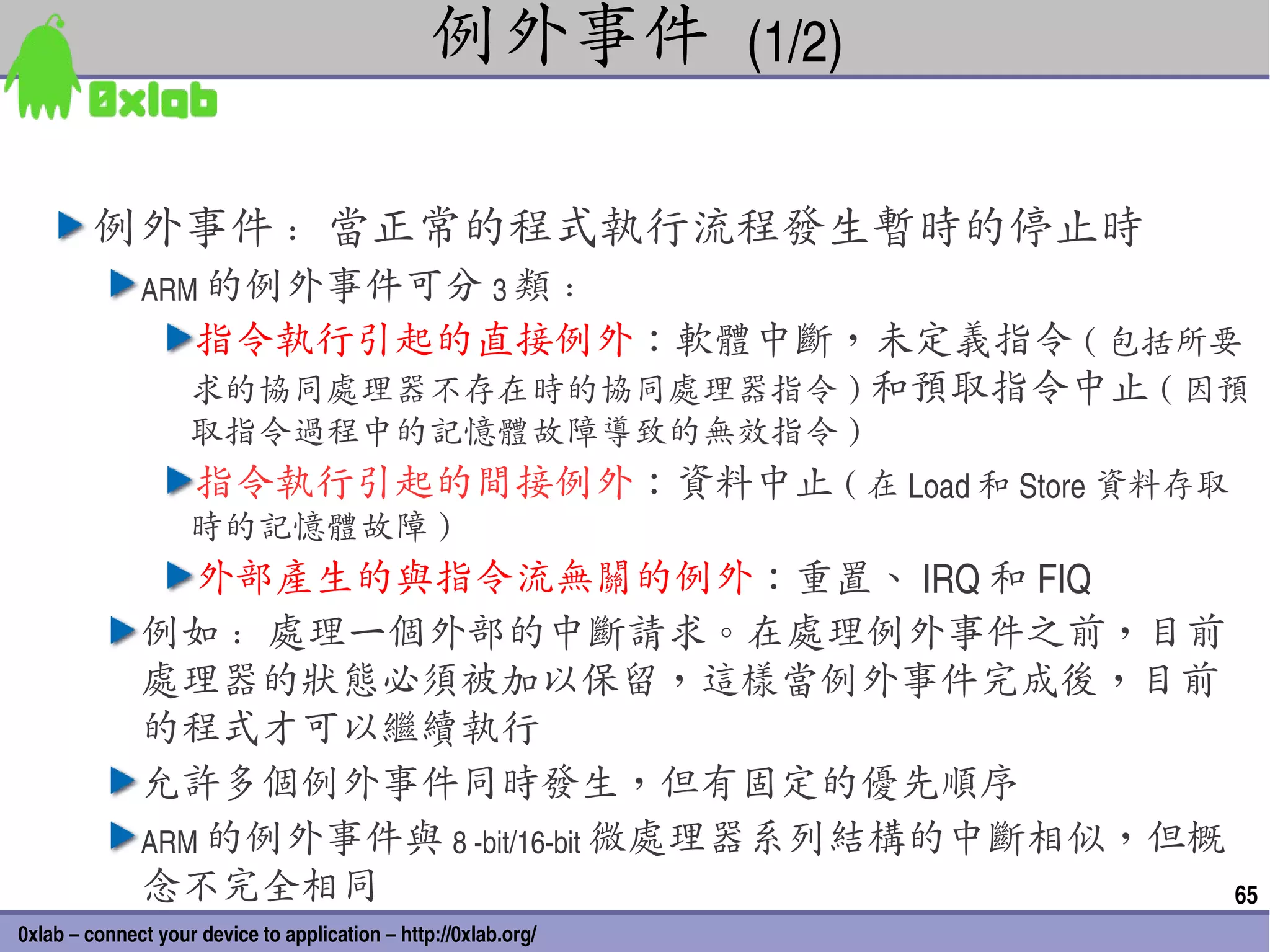
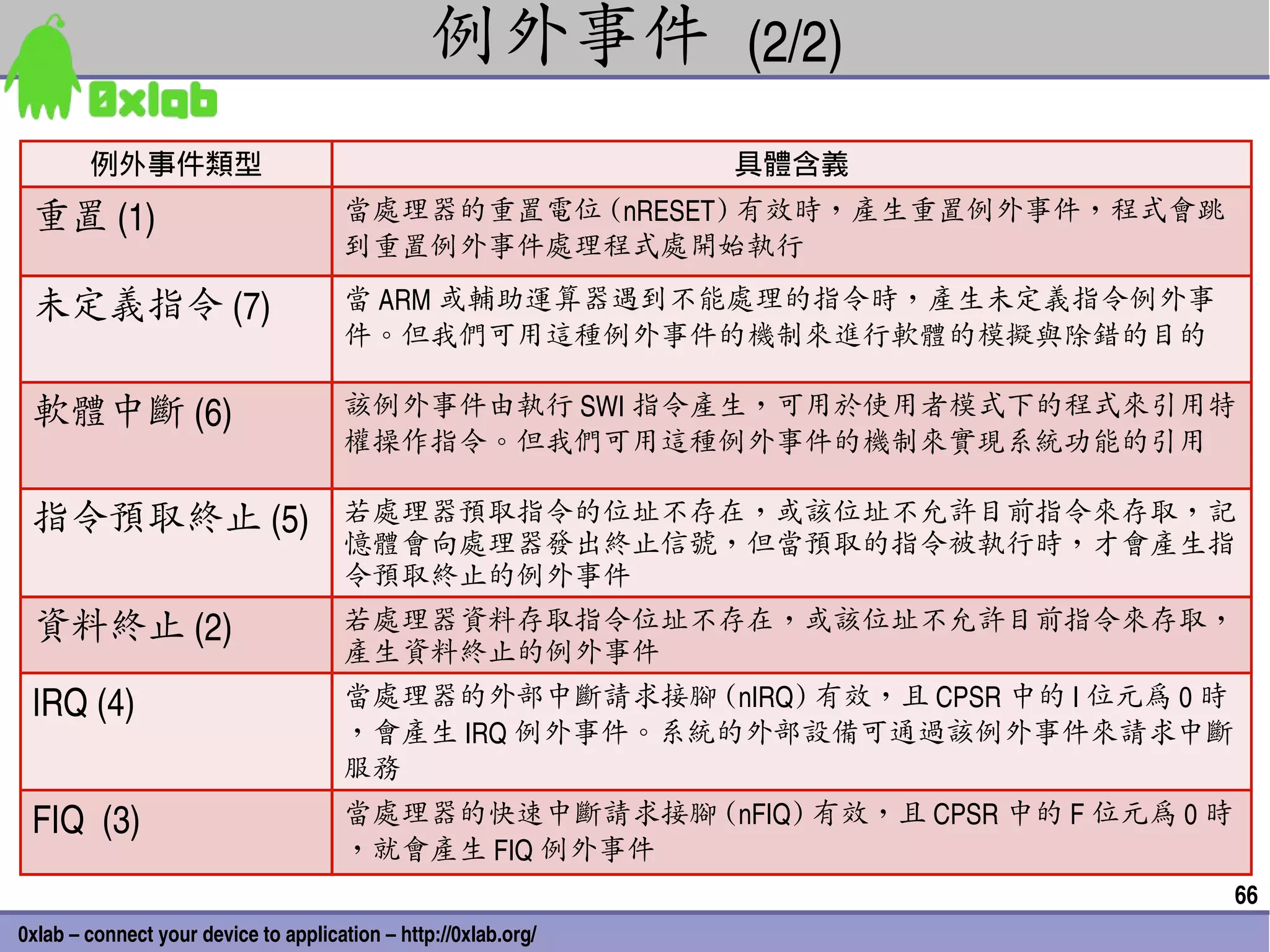
中斷與例外處理
Jim Huang (jserv)
from 0xlab
June 20, 2010
1
0xlab – connect your device to application – http://0xlab.org/
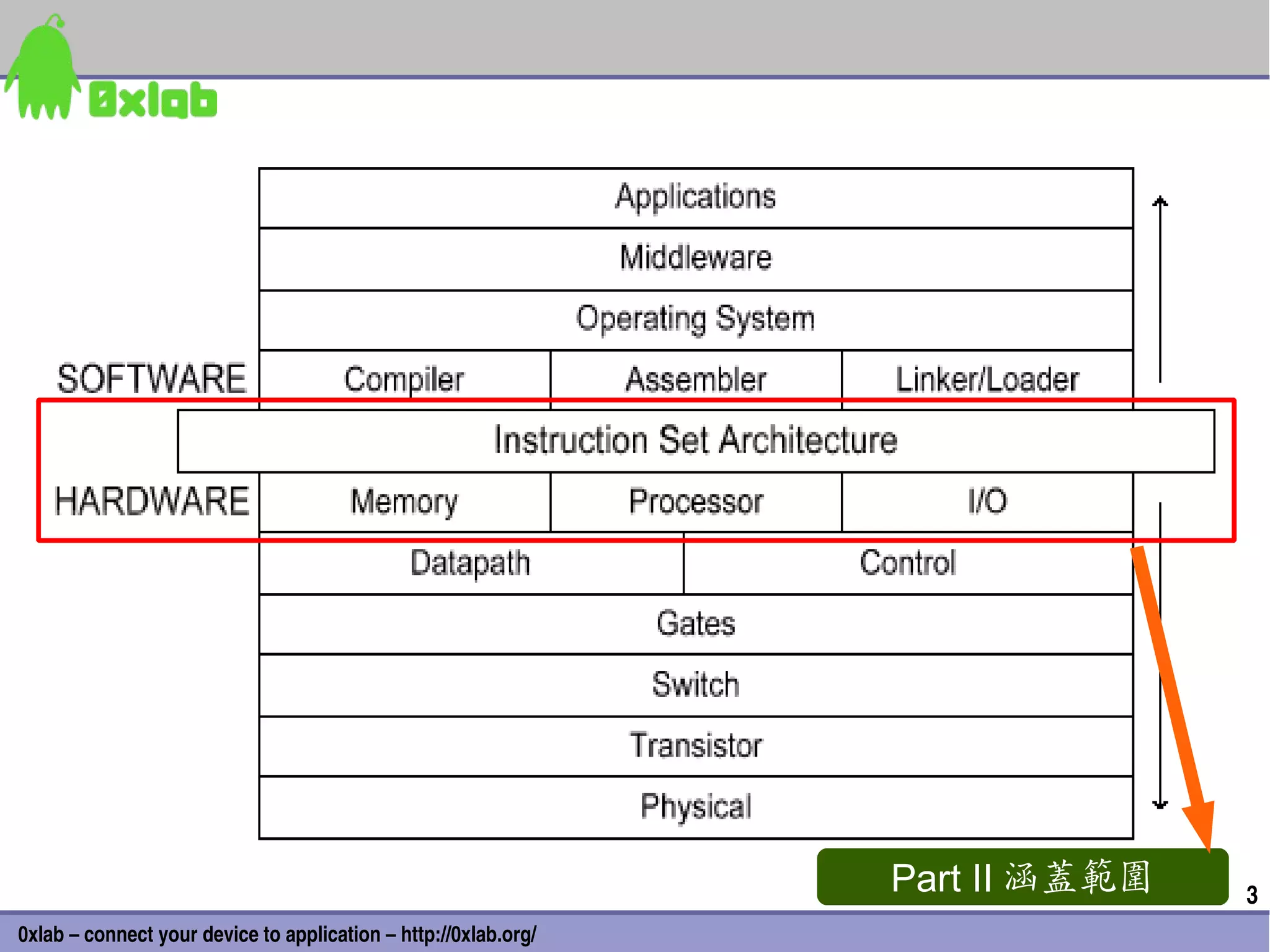
Part II 涵蓋範圍 3
0xlab – connect your device to application – http://0xlab.org/
4.
Agenda
PXA255 SoC 與 CuRT 的硬體啟動程序
ARM Interrupt, ISR, Exception 的處理
ARM 定址與組合語言概況
4
0xlab – connect your device to application – http://0xlab.org/
5.
PXA255 SoC 與 CuRT的硬體啟動程序
ARM Interrupt, ISR, Exception 的處理
ARM 定址與組合語言概況
5
0xlab – connect your device to application – http://0xlab.org/
6.
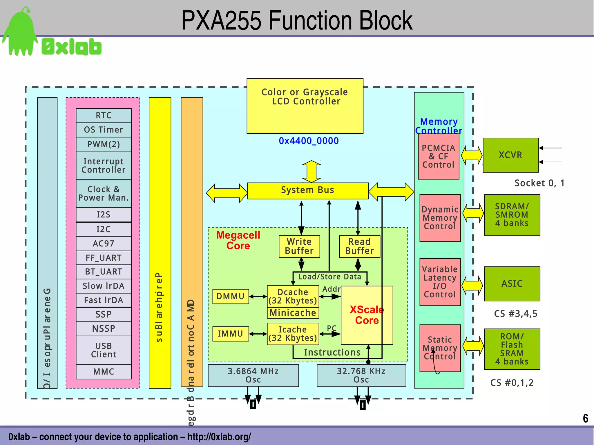
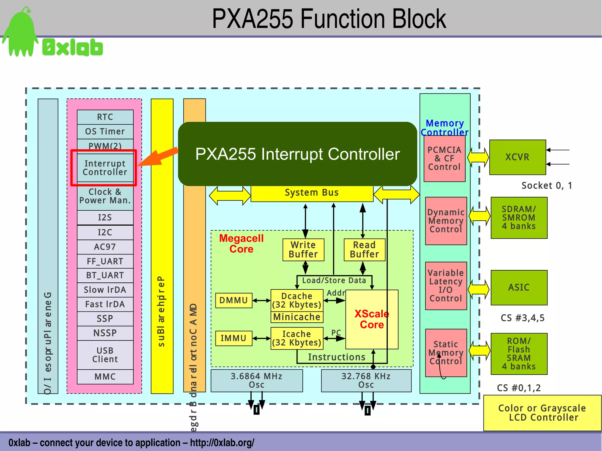
PXA255 Function Block
Color or Grayscale
LCD Controller
RTC
Memory
OS Timer Controller
PWM(2) 0x4400_0000
PCMCIA
& CF XCVR
Interrupt Control
Controller
Socket 0, 1
Clock & System Bus
Power Man.
Dynamic SDRAM/
I2S Memory SMROM
Control 4 banks
I2C
Megacell
AC97 Write Read
Core Buffer Buffer
FF_UART
BT_UART Variable
Load/Store Data
s u B l ar e h p r e P
Latency
Slow lrDA I/O ASIC
Dcac he Addr
O / I es o pr u P l ar e ne G
Control
i
Fast lrDA DMMU
(32 Kbytes)
e g d r B d na r el l ort n o C A MD
SSP Minicache XScale CS #3,4,5
Core
NSSP Icache PC
IMMU ROM/
(32 Kbytes) Static
USB Memory Flash
Client Instructions Control SRAM
4 banks
MMC 3.6864 MHz 32.768 KHz
Osc Osc CS #0,1,2
i
6
0xlab – connect your device to application – http://0xlab.org/
7.
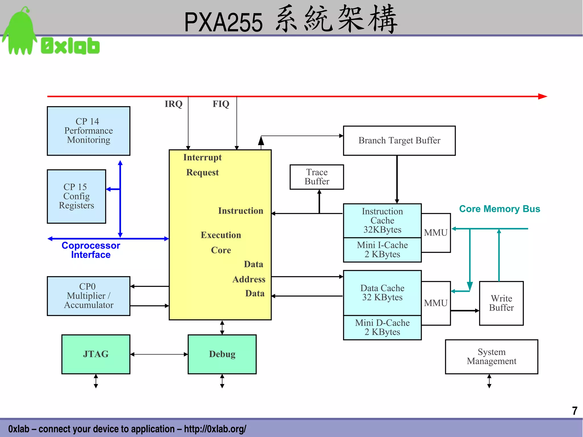
PXA255 系統架構
IRQ FIQ
CP 14
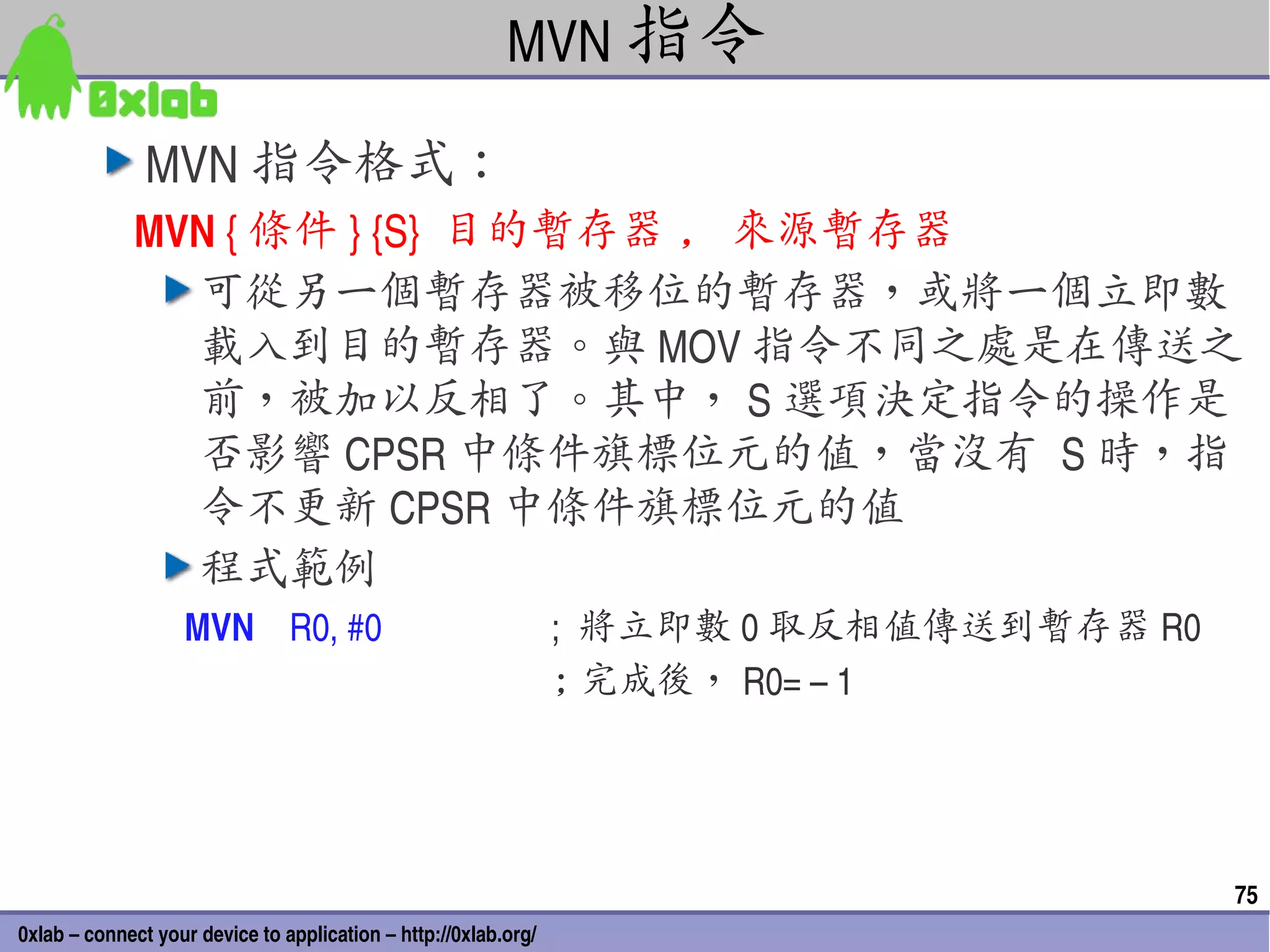
Performance
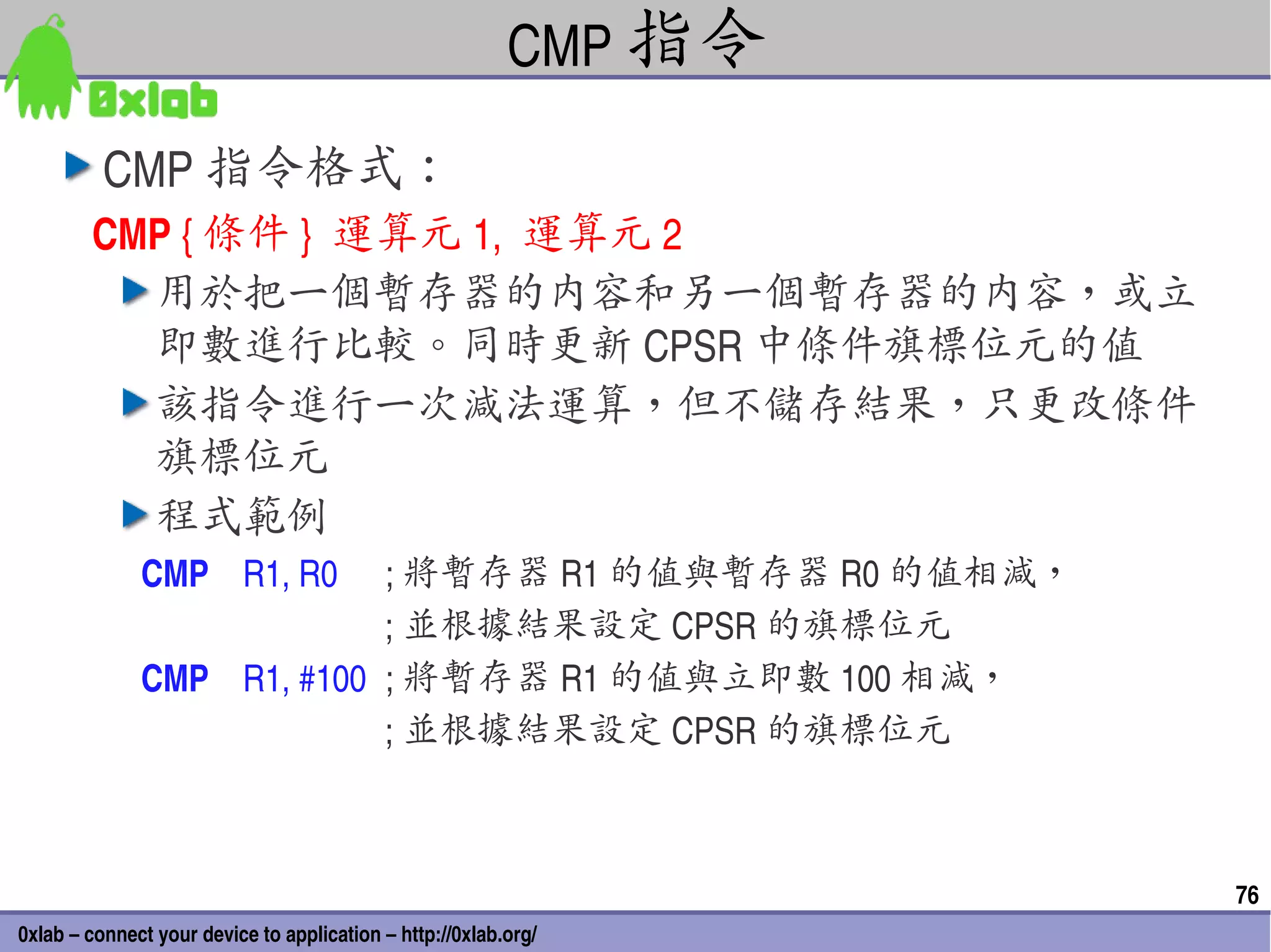
Monitoring Branch Target Buffer
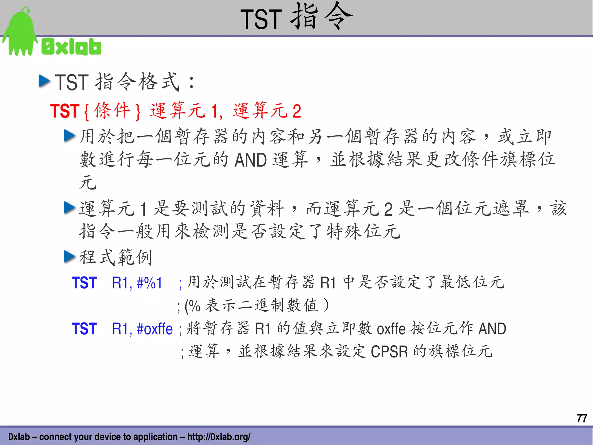
Interrupt
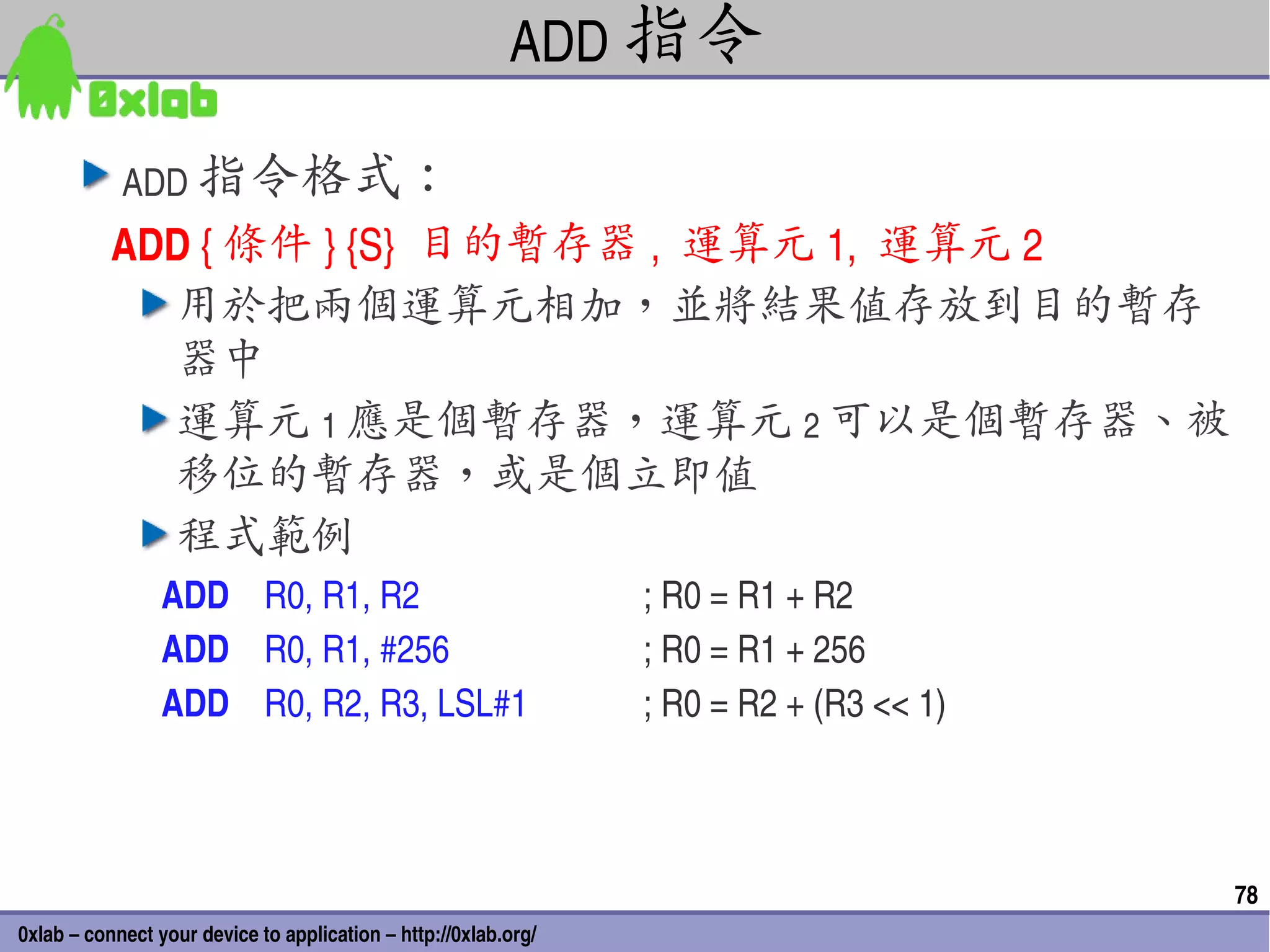
Request Trace
Buffer
CP 15
Config
Registers Core Memory Bus
Instruction Instruction
Cache
32KBytes MMU
Execution
Coprocessor Core
Mini I-Cache
Interface 2 KBytes
Data
Address
CP0 Data Cache
Multiplier / Data 32 KBytes
MMU Write
Accumulator Buffer
Mini D-Cache
2 KBytes
JTAG Debug System
Management
7
0xlab – connect your device to application – http://0xlab.org/
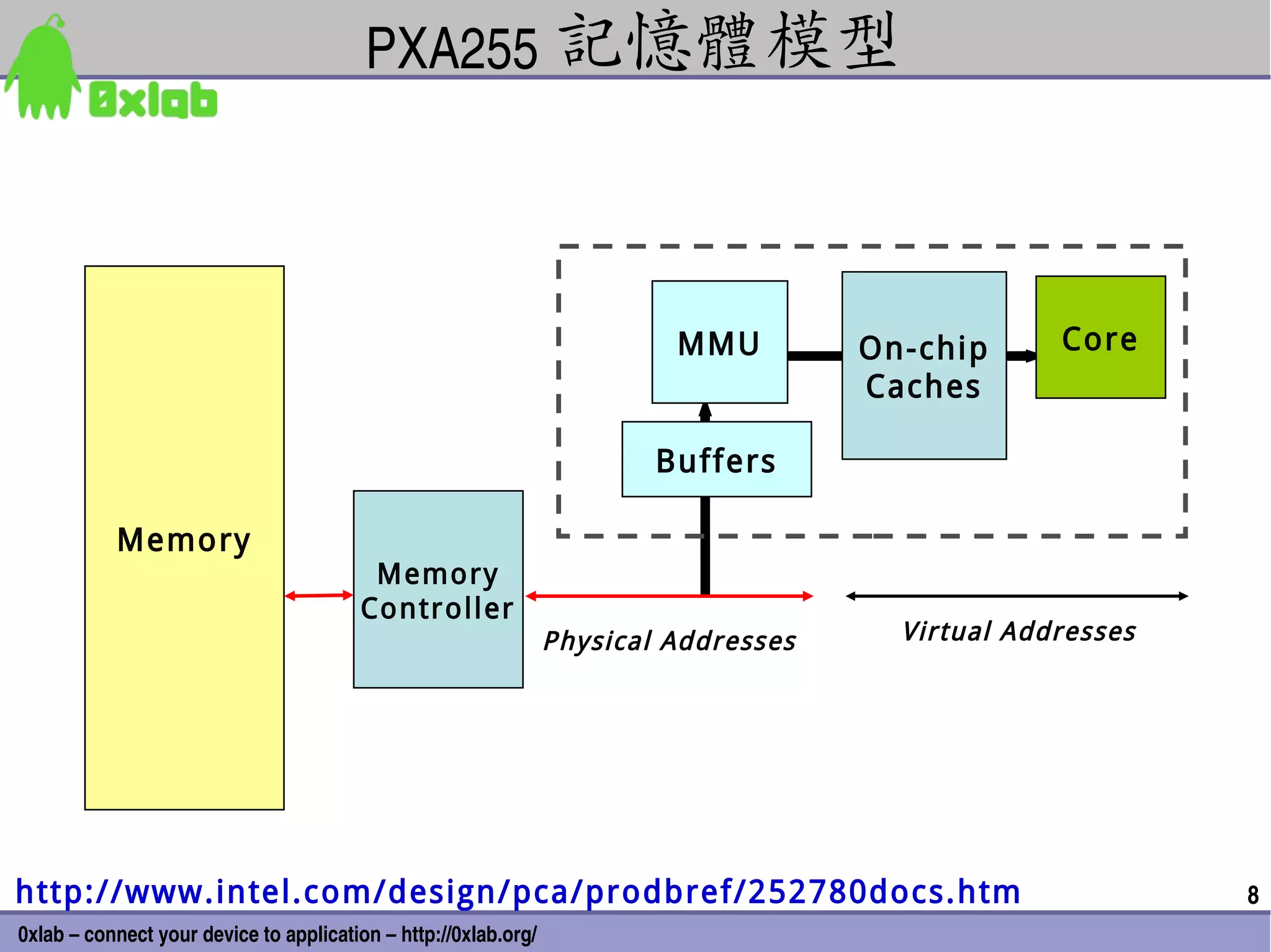
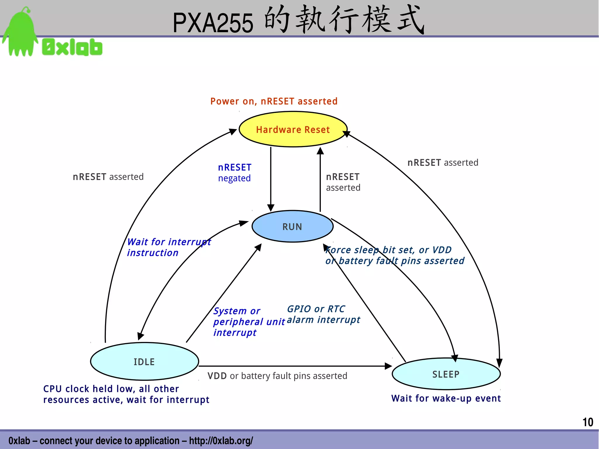
PXA255 的執行模式
Power on, nRESET asserted
Hardware Reset
nRESET asserted
nRESET
nRESET asserted negated nRESET
asserted
RUN
Wait for interrupt
instruction Force sleep bit set, or VDD
or battery fault pins asserted
System or GPIO or RTC
peripheral unit alarm interrupt
interrupt
IDLE
VDD or battery fault pins asserted SLEEP
CPU clock held low, all other
resources active, wait for interrupt Wait for wake-up event
10
0xlab – connect your device to application – http://0xlab.org/
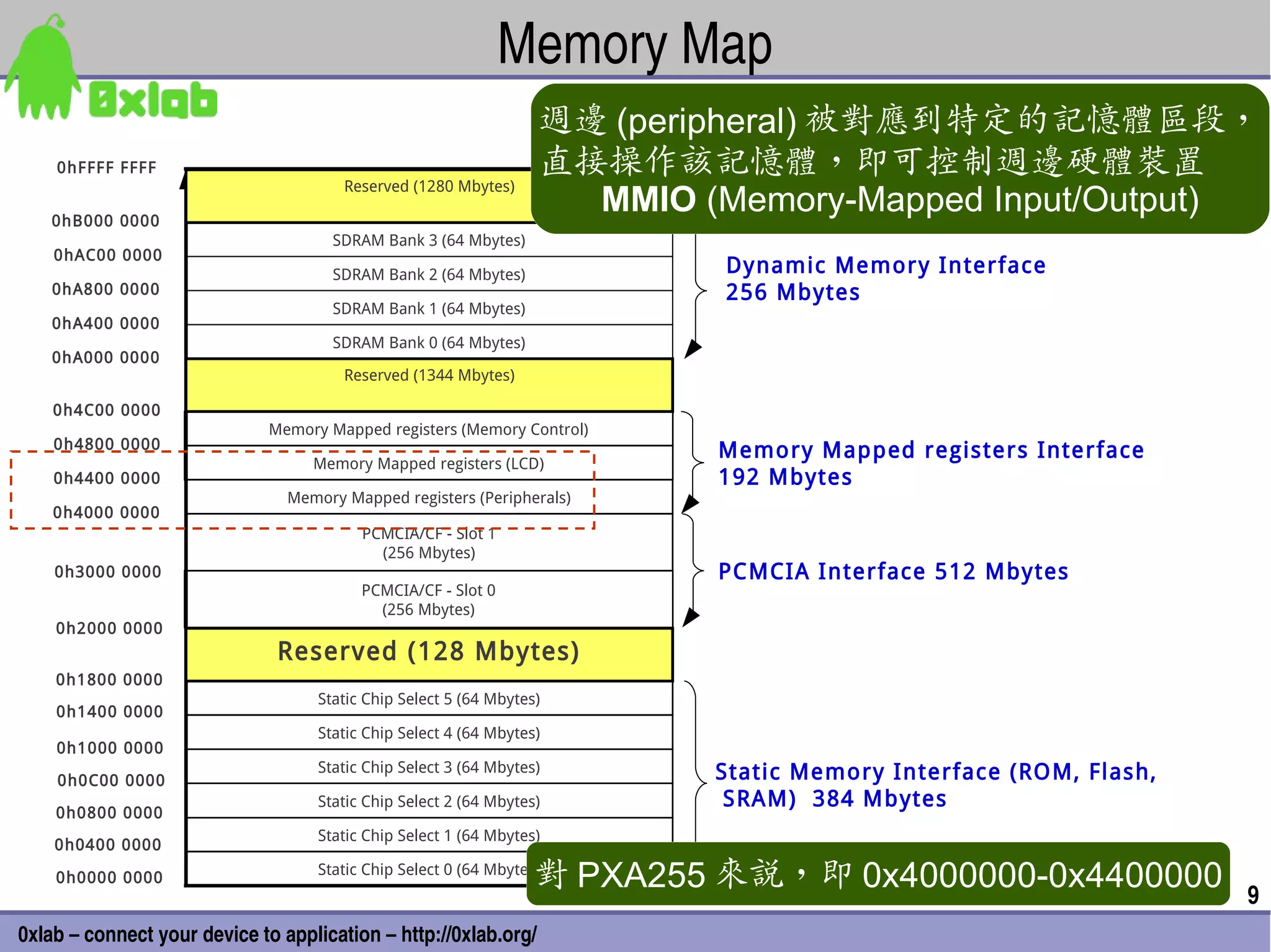
GPIO (General Purpose I/O)
Modem control signals for UART (CTS, RTS, CD, etc) implemented via
GPIO signals
GPIO[58:73] = dual panel color or 16 bit parallel input on LCD
GPIO[23:27] = SPI if both synchronous serial protocols
are required in a single system
Memory
Controller
RTC
O S T ime r
PWM(2) 0x4400_0000 PCMCIA
Inter rupt
& CF XCVR
Contro ller Control
Clo ck & Socket 0, 1
Power Ma n. System Bus
Dynamic SDRAM/
I2S Memory SMROM
I2C Control 4 banks
AC97 Megacell Write Read
FF_U AR T Core B uffe r Buffer
BT_ U ART Variable
Load/Store Data Latency
S low lrD A I/O ASIC
s u B l ar e h p r e P
Dcache Addr
Fast lrD A DMMU (32 Kbytes)
Control
XScale
/ I es o pr u P l ar e n e G
Minicache
i
S SP CS
Core #3,4,5
na r el l ort n o C A MD
NSS P Icache PC
IMMU (32 Kbytes) Static ROM/
U SB Memory Flash
Client Instructions Control SRAM
4 banks
MMC 3.6864 MHz 32.768 KHz
Osc Osc CS #0,1,2
17
0xlab – connect your device to application – http://0xlab.org/
18.
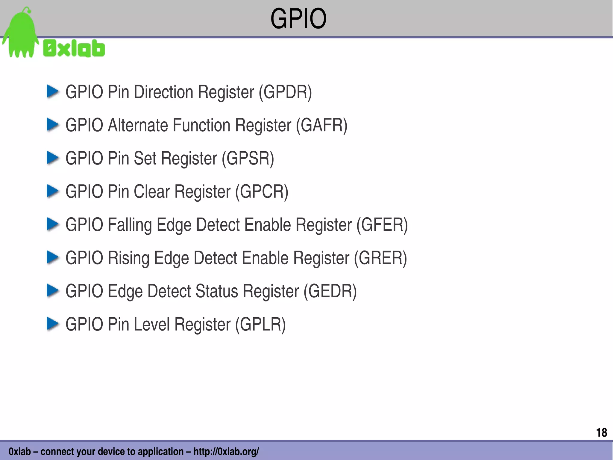
GPIO
GPIO Pin Direction Register (GPDR)
GPIO Alternate Function Register (GAFR)
GPIO Pin Set Register (GPSR)
GPIO Pin Clear Register (GPCR)
GPIO Falling Edge Detect Enable Register (GFER)
GPIO Rising Edge Detect Enable Register (GRER)
GPIO Edge Detect Status Register (GEDR)
GPIO Pin Level Register (GPLR)
18
0xlab – connect your device to application – http://0xlab.org/
19.
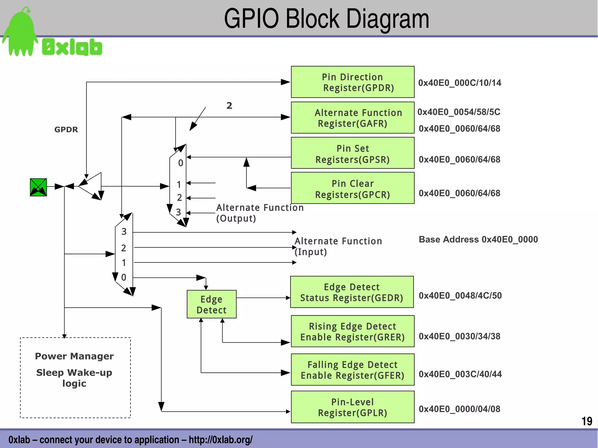
GPIO Block Diagram
Pin Direction
0x40E0_000C/10/14
Register(GPDR)
2
Alternate Function 0x40E0_0054/58/5C
Register(GAFR)
GPDR 0x40E0_0060/64/68
Pin Set
0 Registers(GPSR) 0x40E0_0060/64/68
1 Pin Clear
2 Registers(GPCR) 0x40E0_0060/64/68
Alternate Function
3
(Output)
3
Alternate Function Base Address 0x40E0_0000
2 (Input)
1
0
Edge Detect
Edge Status Register(GEDR) 0x40E0_0048/4C/50
Detect
Rising Edge Detect
Enable Register(GRER) 0x40E0_0030/34/38
Power Manager
Falling Edge Detect
Sleep Wake-up Enable Register(GFER) 0x40E0_003C/40/44
logic
Pin-Level
Register(GPLR) 0x40E0_0000/04/08
19
0xlab – connect your device to application – http://0xlab.org/
20.
CuRT_v1/arch/arm/mach-pxa/start.S
CuRT_v1/arch/arm/mach-pxa/start.S
init_gpio:
init_gpio:
// FFUART
// FFUART
ldr r12, =FFUART_BASE
ldr r12, =FFUART_BASE
ldr
ldr r0,
r0, =0x00000000
=0x00000000
str
str r0,
r0, [r12, #FFLCR]
[r12, #FFLCR]
…
…
//
// First set the output values to a safe/disabled state
First set the output values to a safe/disabled state
//
// before we change any GPIO's outputs start by settings
before we change any GPIO's outputs start by settings
//
// all of them high which is the safest for most signals
all of them high which is the safest for most signals
ldr r12, =GPIO_BASE
ldr r12, =GPIO_BASE
ldr
ldr r0,
r0, =0xffffffff
=0xffffffff
str
str r0,
r0, [r12, #GPIO_GPSR0]
[r12, #GPIO_GPSR0]
str
str r0,
r0, [r12, #GPIO_GPSR1]
[r12, #GPIO_GPSR1]
str
str r0,
r0, [r12, #GPIO_GPSR2]
[r12, #GPIO_GPSR2]
CuRT_v1/includes/arch/arm/mach-pxa/pxa255.h
CuRT_v1/includes/arch/arm/mach-pxa/pxa255.h
/** General Programmable I/O */
/** General Programmable I/O */
#define GPIO_BASE0x40E00000
#define GPIO_BASE0x40E00000
#define GPIO_REG(_x_) *(volatile unsigned long *)(GPIO_BASE + _x_)
#define GPIO_REG(_x_) *(volatile unsigned long *)(GPIO_BASE + _x_)
#define GPIO_GPLR0
#define GPIO_GPLR0 0x00 /* GPIO<31: 0>
0x00 /* GPIO<31: 0> status register */
status register */ 20
#define GPIO_GPLR1
#define GPIO_GPLR1 0x04 /* GPIO<63:32>
0x04 /* GPIO<63:32> status register */
status register */
0xlab – connect your device to application – http://0xlab.org/
#define GPIO_GPLR2
#define GPIO_GPLR2 0x08 /* GPIO<80:64>
0x08 /* GPIO<80:64> status register */
status register */
21.
Register Register
GPIO[15:0] GPIO[31:16] GPIO[47:32] GPIO[63:48] GPIO[79:64] GPIO[80]
Type Function
GPLR Monitor Pin State GPLR0 GPLR1 GPLR2
GPSR GPSR0 GPSR1 GPSR2
Control Output
Pin State
GPCR GPCR0 GPCR1 GPCR2
GPDR Set Pin Direction GPDR0 GPDR1 GPDR2
GRER GRER0 GRER1 GRER2
Detect Rising/
Falling Edge
GFER GFER0 GFER1 GFER2
GEDR Detect Edge Type GEDR0 GEDR1 GEDR2
Set Alternate
GAFR GAFR0_L GAFR0_U GAFR1_L GAFR1_U GAFR2_L GAFR2_U
Functions
21
0xlab – connect your device to application – http://0xlab.org/
22.
PXA255 SoC 與 CuRT的硬體啟動程序
ARM Interrupt, ISR, Exception 的處理
ARM 定址與組合語言概況
22
0xlab – connect your device to application – http://0xlab.org/
23.
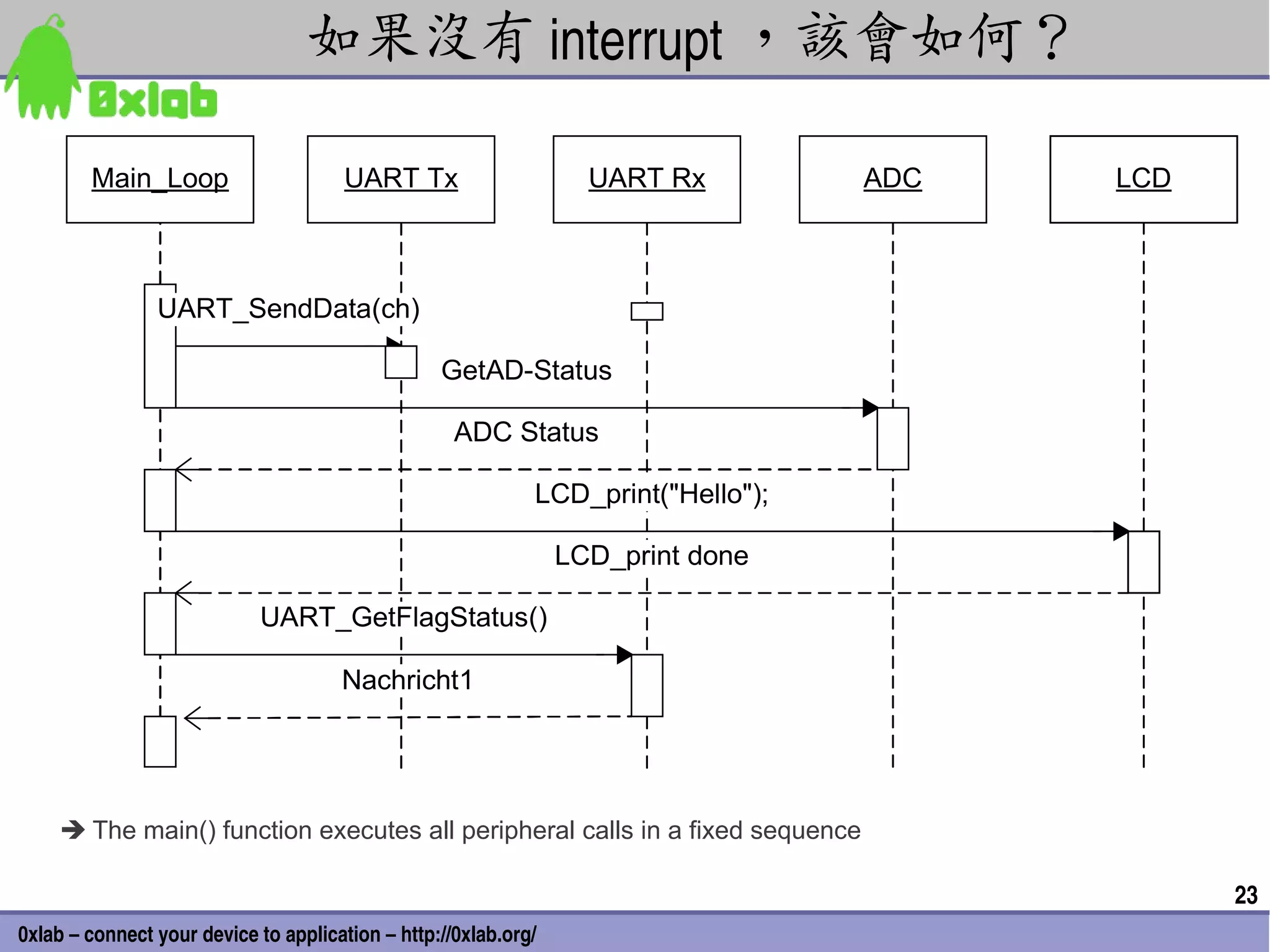
如果沒有 interrupt ,該會如何?
Main_Loop UART Tx UART Rx ADC LCD
UART_SendData(ch)
GetAD-Status
ADC Status
LCD_print("Hello");
LCD_print done
UART_GetFlagStatus()
Nachricht1
The main() function executes all peripheral calls in a fixed sequence
23
0xlab – connect your device to application – http://0xlab.org/
24.
interrupt 的定義與特性
Interrupts are asynchronous events that may happen any time
Interrupts stop the execution of the current task
The processor jumps into the interrupt service routine (ISR)
The short ISR is executed
Control is given back to the previously executing task
Interrupts may have priorities.
Concurrent interrupts (interrupts that happen at the same time)
are serviced according to their priority
Interrupts may be enabled or disabled
Library functions that may be executed by an ISR must be
thread-safe (they have to adhere to some specific rules)
An ISR should if possible not trigger another interrupt
24
0xlab – connect your device to application – http://0xlab.org/
25.
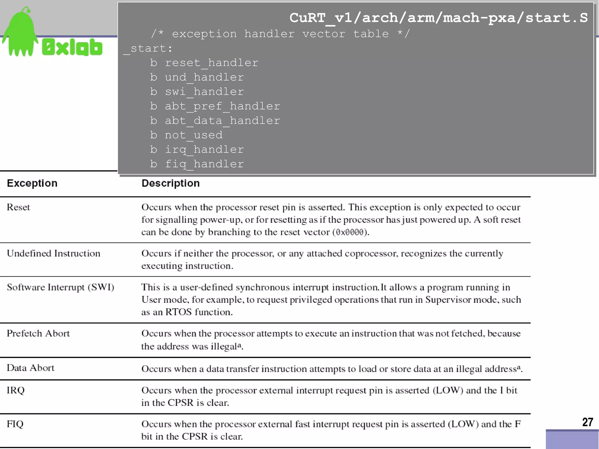
ARM Interrupt Controller
All interrupts routed to FIQ or IRQ
Two level interrupt structure
What module caused interrupt
Serial channel, DMA, Power Management, etc
Why did an interrupt occur there?
RX, TX, overrun, underrun, Data Done, Battery Fault, etc
Template for servicing interrupts provided with firmware
Peripheral/PCMCIA interrupt mask in each module
GPIO masks determined per pin or group of pins
25
0xlab – connect your device to application – http://0xlab.org/
26.
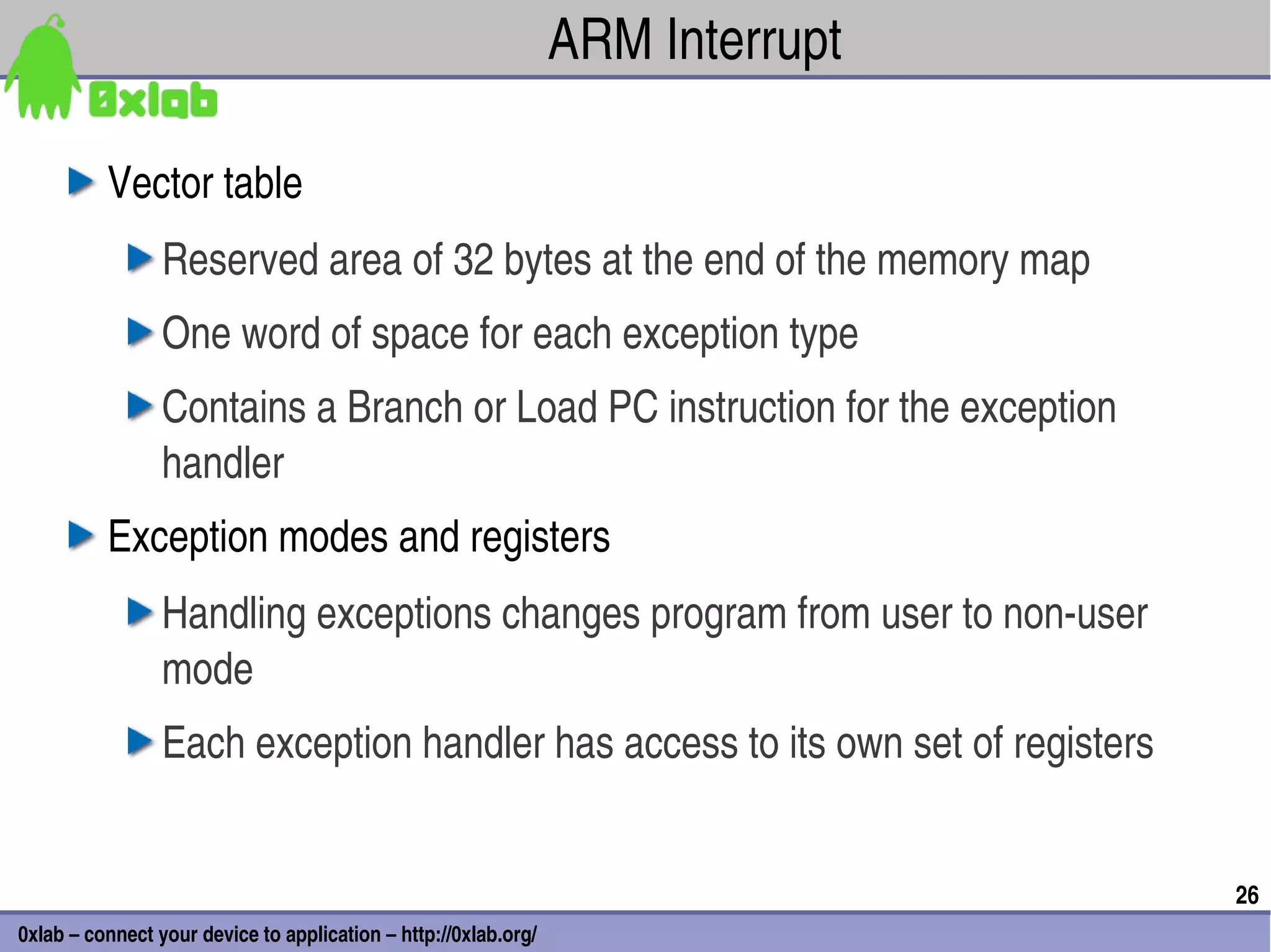
ARM Interrupt
Vector table
Reserved area of 32 bytes at the end of the memory map
One word of space for each exception type
Contains a Branch or Load PC instruction for the exception
handler
Exception modes and registers
Handling exceptions changes program from user to nonuser
mode
Each exception handler has access to its own set of registers
26
0xlab – connect your device to application – http://0xlab.org/
27.
CuRT_v1/arch/arm/mach-pxa/start.S
CuRT_v1/arch/arm/mach-pxa/start.S
/* exception handler vector table */
/* exception handler vector table */
_start:
_start:
b reset_handler
b reset_handler
b und_handler
b und_handler
b swi_handler
b swi_handler
b abt_pref_handler
b abt_pref_handler
b abt_data_handler
b abt_data_handler
b not_used
b not_used
b irq_handler
b irq_handler
b fiq_handler
b fiq_handler
27
0xlab – connect your device to application – http://0xlab.org/
28.
CuRT_v1/arch/arm/mach-pxa/start.S
CuRT_v1/arch/arm/mach-pxa/start.S
/* exception handler vector table */
/* exception handler vector table */
_start:
_start:
b reset_handler
b reset_handler
b und_handler
b und_handler
b swi_handler
b swi_handler
b abt_pref_handler
b abt_pref_handler
b abt_data_handler
b abt_data_handler 如果 Exceptions 同時發生,
b not_used
b not_used
b irq_handler
b irq_handler
會如何?
b fiq_handler
b fiq_handler
28
0xlab – connect your device to application – http://0xlab.org/
IRQ 與 FIQ
• Program Status Register
31 30 29 28 27 … 8 7 6 5 4 3 2 1 0
N Z C V I F M4 M3 M2 M1 M0
– 若要抑制 interrupts ,將 "F” 或“ I” bit 設定為 1
• 一旦 interrupt 觸發,處理器將變更至 FIQ32_mode registers 或
IRQ32_mode registers
• Switch register banks
• Copies CPSR to SPSR_mode (saves mode, interrupt flags, etc.)
• Changes the CPSR mode bits (M[4:0])
• Disables interrupts
• Copies PC to R14_mode (to provide return address)
• Sets the PC to the vector address of the exception handler
30
0xlab – connect your device to application – http://0xlab.org/
31.
CuRT_v1/arch/arm/mach-pxa/arm_port.S
CuRT_v1/arch/arm/mach-pxa/arm_port.S
irq_service_routine:
irq_service_routine:
msr CPSR_c, #(NO_INT | IRQ32_MODE)
msr CPSR_c, #(NO_INT | IRQ32_MODE)
stmfd sp!, {r1-r3}
stmfd sp!, {r1-r3} // push working registers onto IRQ stack
// push working registers onto IRQ stack
mov r1, sp
mov r1, sp // save IRQ stack pointer
// save IRQ stack pointer
add sp, sp, #12
add sp, sp, #12 // adjust IRQ stack pointer
// adjust IRQ stack pointer
sub r2, lr, #4
sub r2, lr, #4 // adjust pc for return
// adjust pc for return
mrs
mrs r3, SPSR
r3, SPSR // copy SPSR (interrupted thread's CPSR)
// copy SPSR (interrupted thread's CPSR)
msr
msr CPSR_c, #(NO_INT | SVC32_MODE)
CPSR_c, #(NO_INT | SVC32_MODE) // change to SVC mode
// change to SVC mode
// save thread's context onto thread's stack
// save thread's context onto thread's stack
stmfd
stmfd sp!,
sp!, {r2}
{r2} // push thread's return pc
// push thread's return pc
stmfd
stmfd sp!,
sp!, {lr}
{lr} // push thread's LR
// push thread's LR
stmfd
stmfd sp!,
sp!, {r4-r12}
{r4-r12} // push thread's r12-r4
// push thread's r12-r4
ldmfd r1!, {r4-r6}
ldmfd r1!, {r4-r6} // move thread's r1-r3 from IRQ stack to
// move thread's r1-r3 from IRQ stack to
// SVC stack
// SVC stack
stmfd sp!, {r4-r6}
stmfd sp!, {r4-r6}
stmfd sp!, {r0}
stmfd sp!, {r0} // push thread's r0 onto thread's stack
// push thread's r0 onto thread's stack
stmfd sp!, {r3}
stmfd sp!, {r3} // push thread's CPSR(IRQ's SPSR)
// push thread's CPSR(IRQ's SPSR)
bl enter_interrupt • 一旦 interrupt 觸發,處理器將變更至 FIQ32_mode registers 或 IRQ32_mode registers
bl enter_interrupt
... • Switch register banks
...
• Copies CPSR to SPSR_mode (saves mode, interrupt flags, etc.)
• Changes the CPSR mode bits (M[4:0])
• Disables interrupts
• Copies PC to R14_mode (to provide return address)
• Sets the PC to the vector address of the exception handler
31
0xlab – connect your device to application – http://0xlab.org/
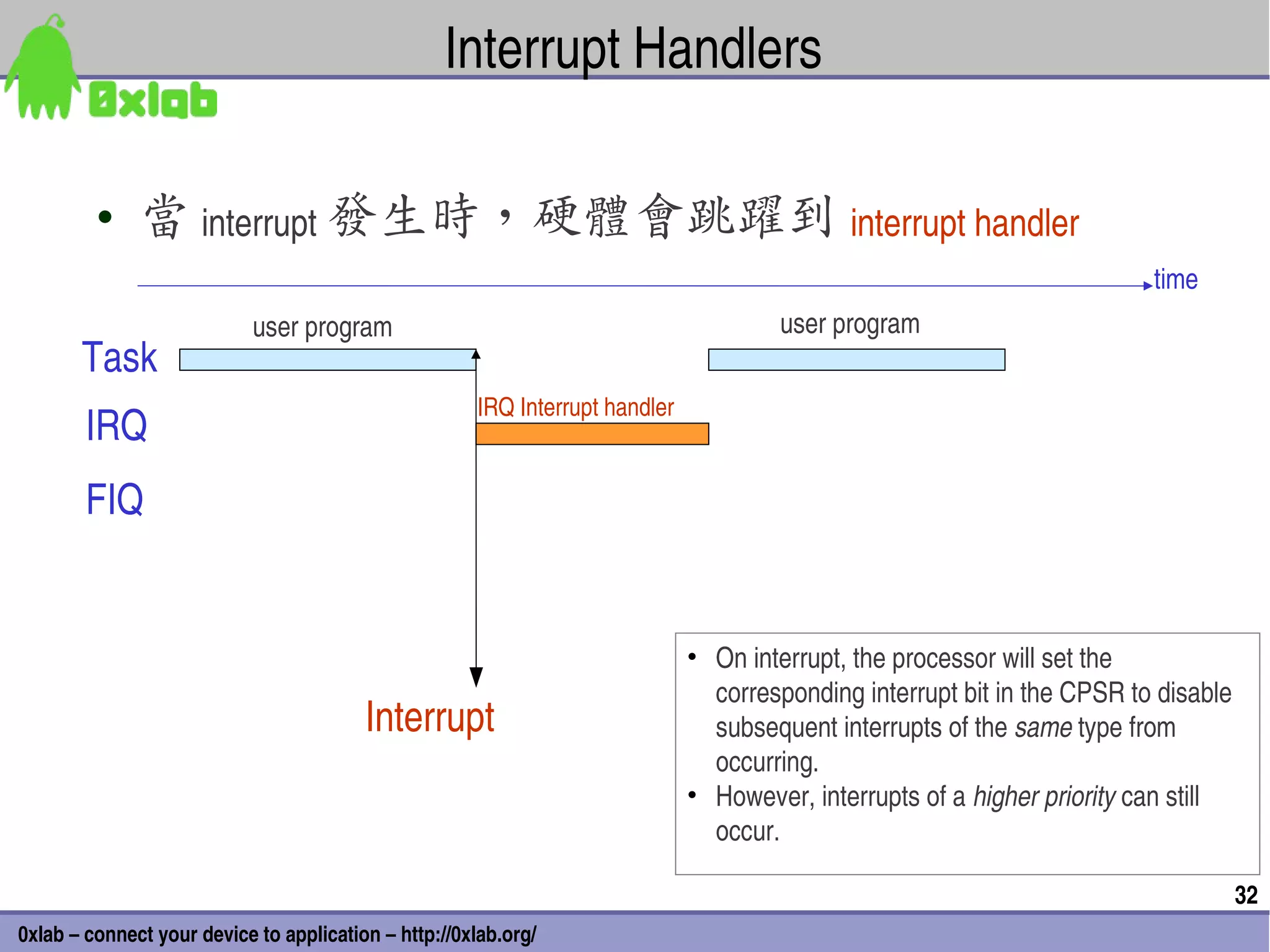
32.
Interrupt Handlers
• 當 interrupt 發生時,硬體會跳躍到 interrupt handler
time
user program user program
Task
IRQ Interrupt handler
IRQ
FIQ
• On interrupt, the processor will set the
corresponding interrupt bit in the CPSR to disable
Interrupt subsequent interrupts of the same type from
occurring.
• However, interrupts of a higher priority can still
occur.
32
0xlab – connect your device to application – http://0xlab.org/
33.
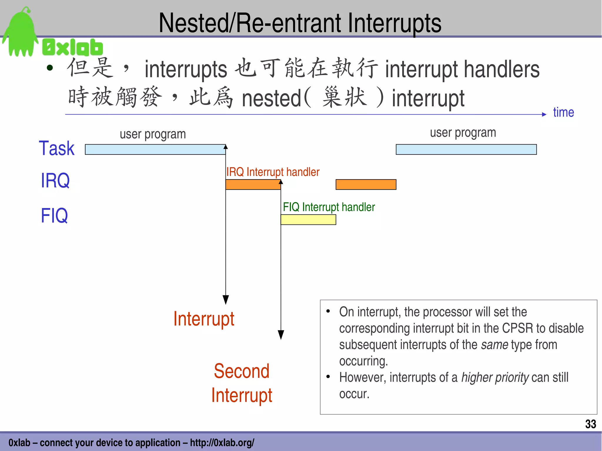
Nested/Reentrant Interrupts
• 但是, interrupts 也可能在執行 interrupt handlers
時被觸發,此為 nested( 巢狀 ) interrupt time
user program user program
Task
IRQ Interrupt handler
IRQ
FIQ Interrupt handler
FIQ
• On interrupt, the processor will set the
Interrupt corresponding interrupt bit in the CPSR to disable
subsequent interrupts of the same type from
occurring.
Second • However, interrupts of a higher priority can still
Interrupt occur.
33
0xlab – connect your device to application – http://0xlab.org/
34.
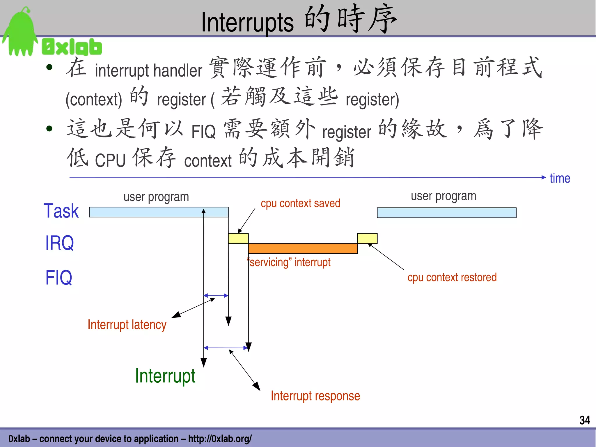
Interrupts 的時序
• 在 interrupt handler 實際運作前,必須保存目前程式
(context) 的 register ( 若觸及這些 register)
• 這也是何以 FIQ 需要額外 register 的緣故,為了降
低 CPU 保存 context 的成本開銷
time
user program user program
cpu context saved
Task
IRQ
“servicing” interrupt
FIQ cpu context restored
Interrupt latency
Interrupt
Interrupt response
34
0xlab – connect your device to application – http://0xlab.org/
35.
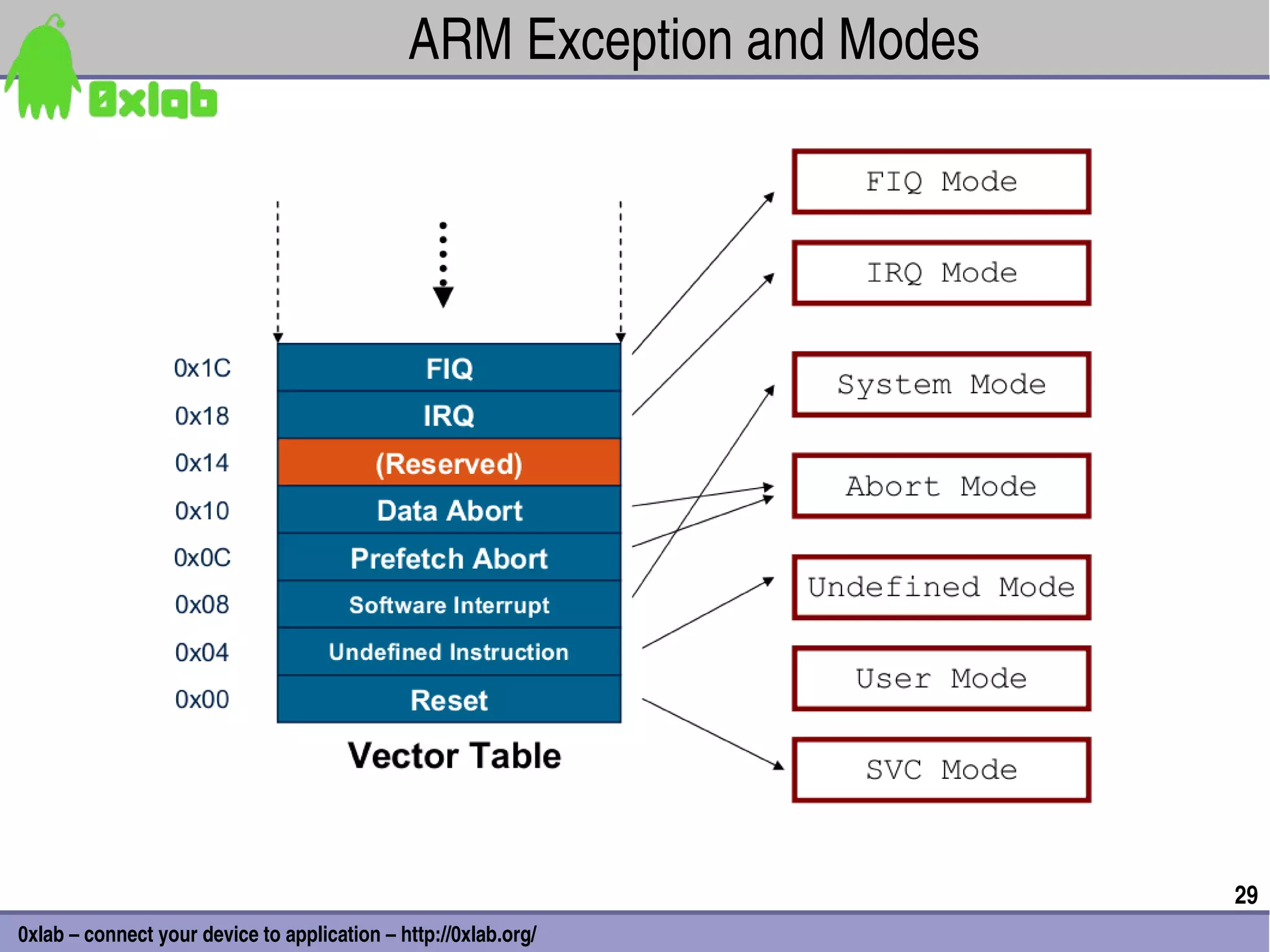
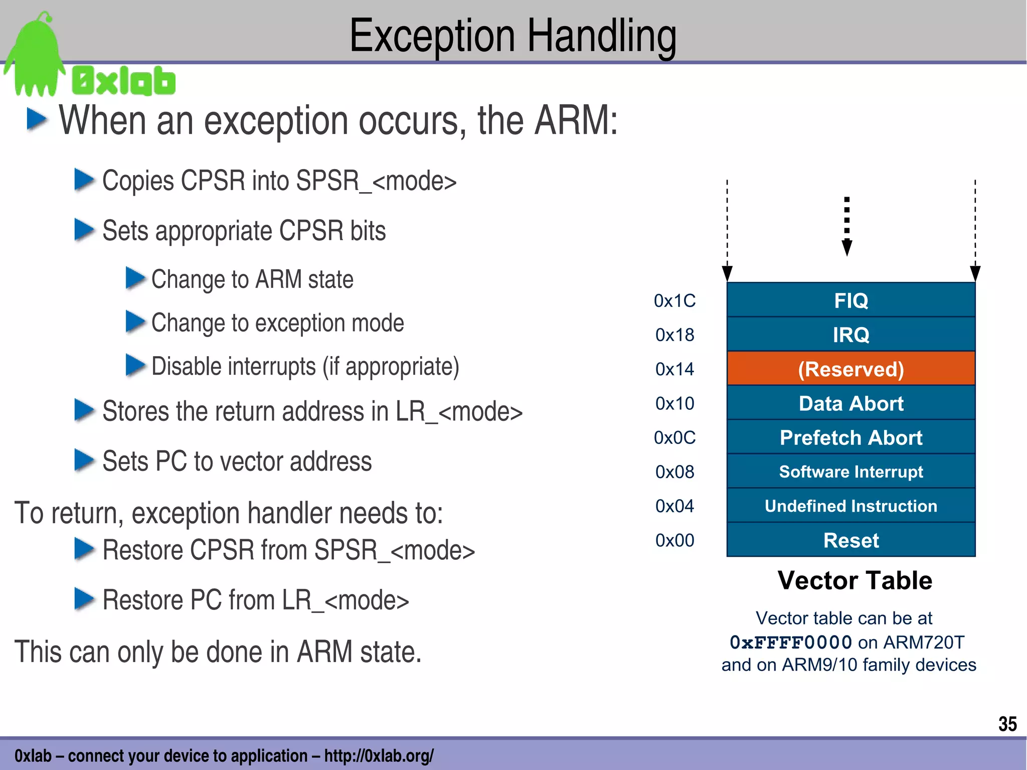
Exception Handling
When an exception occurs, the ARM:
Copies CPSR into SPSR_<mode>
Sets appropriate CPSR bits
Change to ARM state
0x1C FIQ
Change to exception mode 0x18 IRQ
Disable interrupts (if appropriate) 0x14 (Reserved)
Stores the return address in LR_<mode> 0x10 Data Abort
0x0C Prefetch Abort
Sets PC to vector address 0x08 Software Interrupt
To return, exception handler needs to: 0x04 Undefined Instruction
0x00 Reset
Restore CPSR from SPSR_<mode>
Vector Table
Restore PC from LR_<mode>
Vector table can be at
0xFFFF0000 on ARM720T
This can only be done in ARM state. and on ARM9/10 family devices
35
0xlab – connect your device to application – http://0xlab.org/
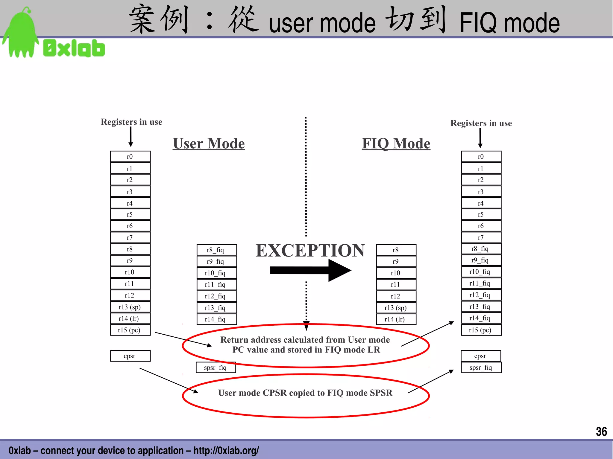
36.
案例:從 user mode 切到FIQ mode
Registers in use Registers in use
User Mode FIQ Mode
r0 r0
r1 r1
r2 r2
r3 r3
r4 r4
r5 r5
r6 r6
r7 r7
r8
r9
r8_fiq
r9_fiq
EXCEPTION r8
r9
r8_fiq
r9_fiq
r10 r10_fiq r10 r10_fiq
r11 r11_fiq r11 r11_fiq
r12 r12_fiq r12 r12_fiq
r13 (sp) r13_fiq r13 (sp) r13_fiq
r14 (lr) r14_fiq r14 (lr) r14_fiq
r15 (pc) r15 (pc)
Return address calculated from User mode
PC value and stored in FIQ mode LR
cpsr cpsr
spsr_fiq spsr_fiq
User mode CPSR copied to FIQ mode SPSR
36
0xlab – connect your device to application – http://0xlab.org/
PXA255 Function Block
RTC
Memory
OS Timer Controller
PWM(2) 0x4400_0000
Interrupt
PXA255 Interrupt Controller PCMCIA
& CF XCVR
Control
Controller
Socket 0, 1
Clock & System Bus
Power Man.
Dynamic SDRAM/
I2S Memory SMROM
Control 4 banks
I2C
Megacell
AC97 Write Read
Core Buffer Buffer
FF_UART
BT_UART Variable
Load/Store Data
s u B l ar e h p r e P
Latency
Slow lrDA I/O ASIC
Dcac he Addr
O / I es o pr u P l ar e ne G
Control
i
Fast lrDA DMMU
(32 Kbytes)
e g d r B d na r el l ort n o C A MD
SSP Minicache XScale CS #3,4,5
Core
NSSP Icache PC
IMMU ROM/
(32 Kbytes) Static
USB Memory Flash
Client Instructions Control SRAM
4 banks
MMC 3.6864 MHz 32.768 KHz
Osc Osc CS #0,1,2
Color or Grayscale
LCD Controller
i
38
0xlab – connect your device to application – http://0xlab.org/
PXA255 SoC 與 CuRT的硬體啟動程序
ARM Interrupt, ISR, Exception 的處理
ARM 定址與組合語言概況
43
0xlab – connect your device to application – http://0xlab.org/
44.
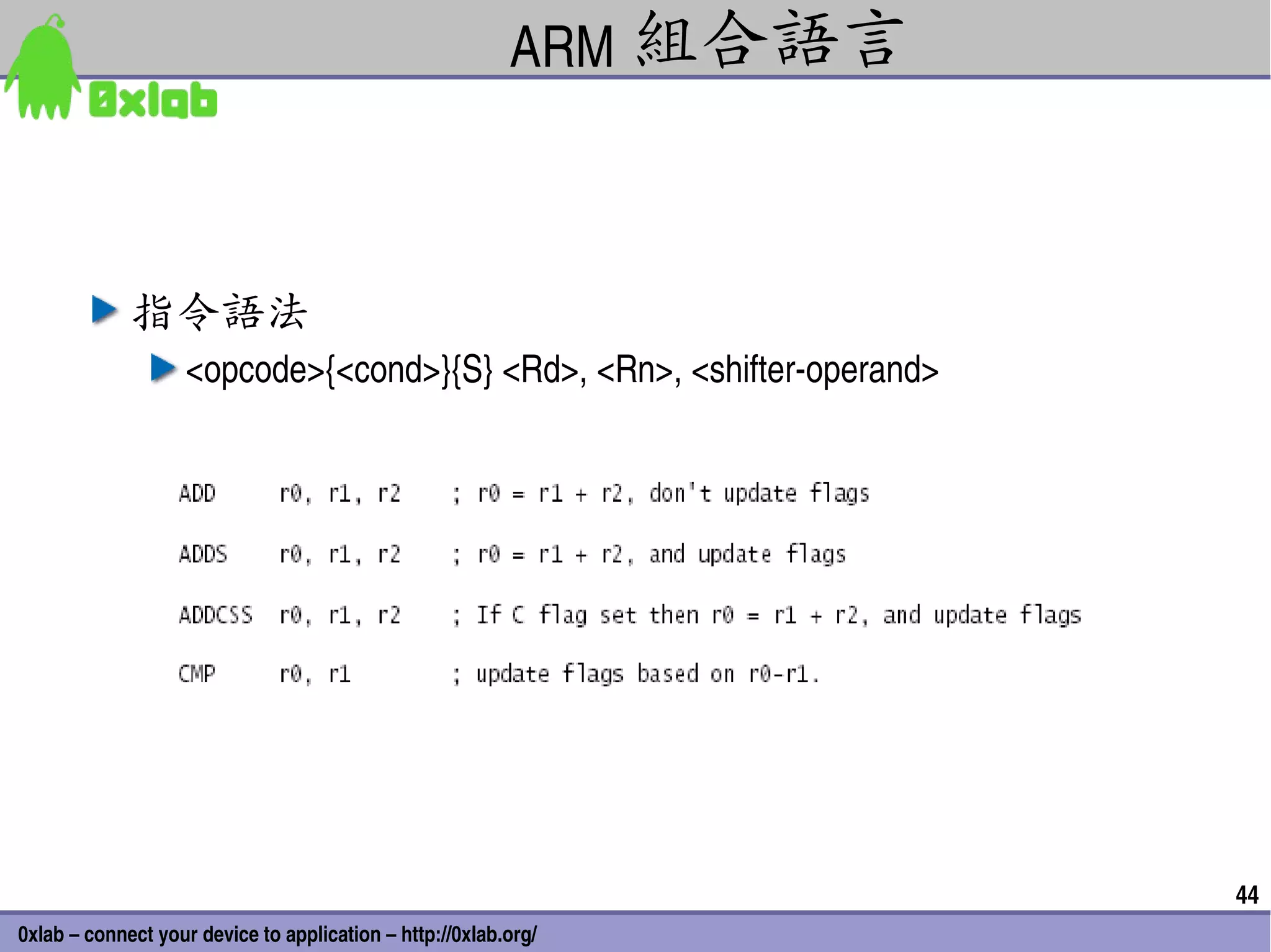
ARM 組合語言
指令語法
<opcode>{<cond>}{S} <Rd>, <Rn>, <shifteroperand>
44
0xlab – connect your device to application – http://0xlab.org/
45.
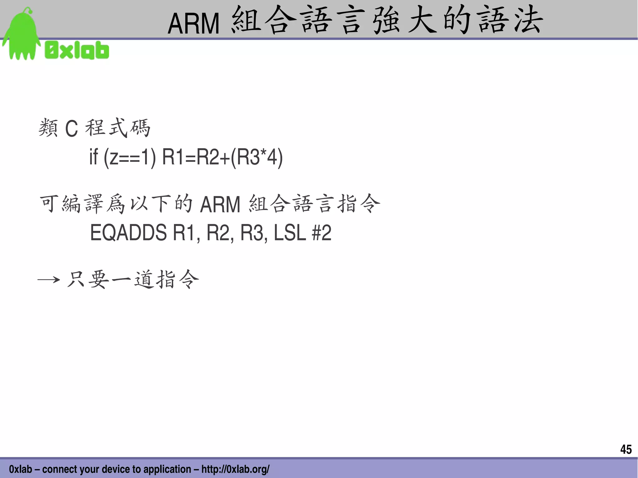
ARM 組合語言強大的語法
類 C 程式碼
if (z==1) R1=R2+(R3*4)
可編譯為以下的 ARM 組合語言指令
EQADDS R1, R2, R3, LSL #2
→ 只要一道指令
45
0xlab – connect your device to application – http://0xlab.org/
46.
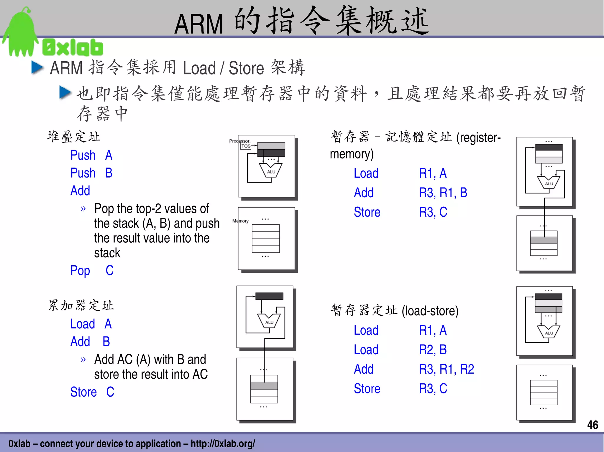
ARM 的指令集概述
ARM 指令集採用 Load / Store 架構
也即指令集僅能處理暫存器中的資料,且處理結果都要再放回暫
存器中
堆疊定址 暫存器 - 記憶體定址 (register
Push A memory)
Push B Load R1, A
Add Add R3, R1, B
» Pop the top2 values of Store R3, C
the stack (A, B) and push
the result value into the
stack
Pop C
累加器定址 暫存器定址 (loadstore)
Load A Load R1, A
Add B
Load R2, B
» Add AC (A) with B and
store the result into AC Add R3, R1, R2
Store C Store R3, C
46
0xlab – connect your device to application – http://0xlab.org/
47.
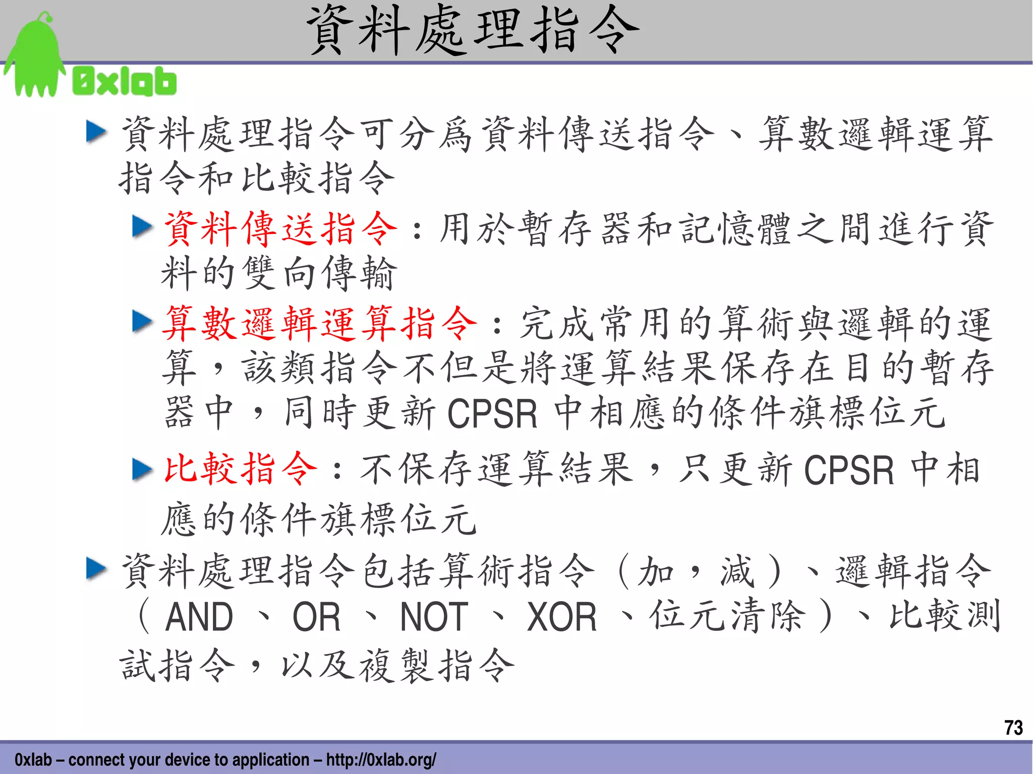
ARM 指令集概述
ARM 指令集分為
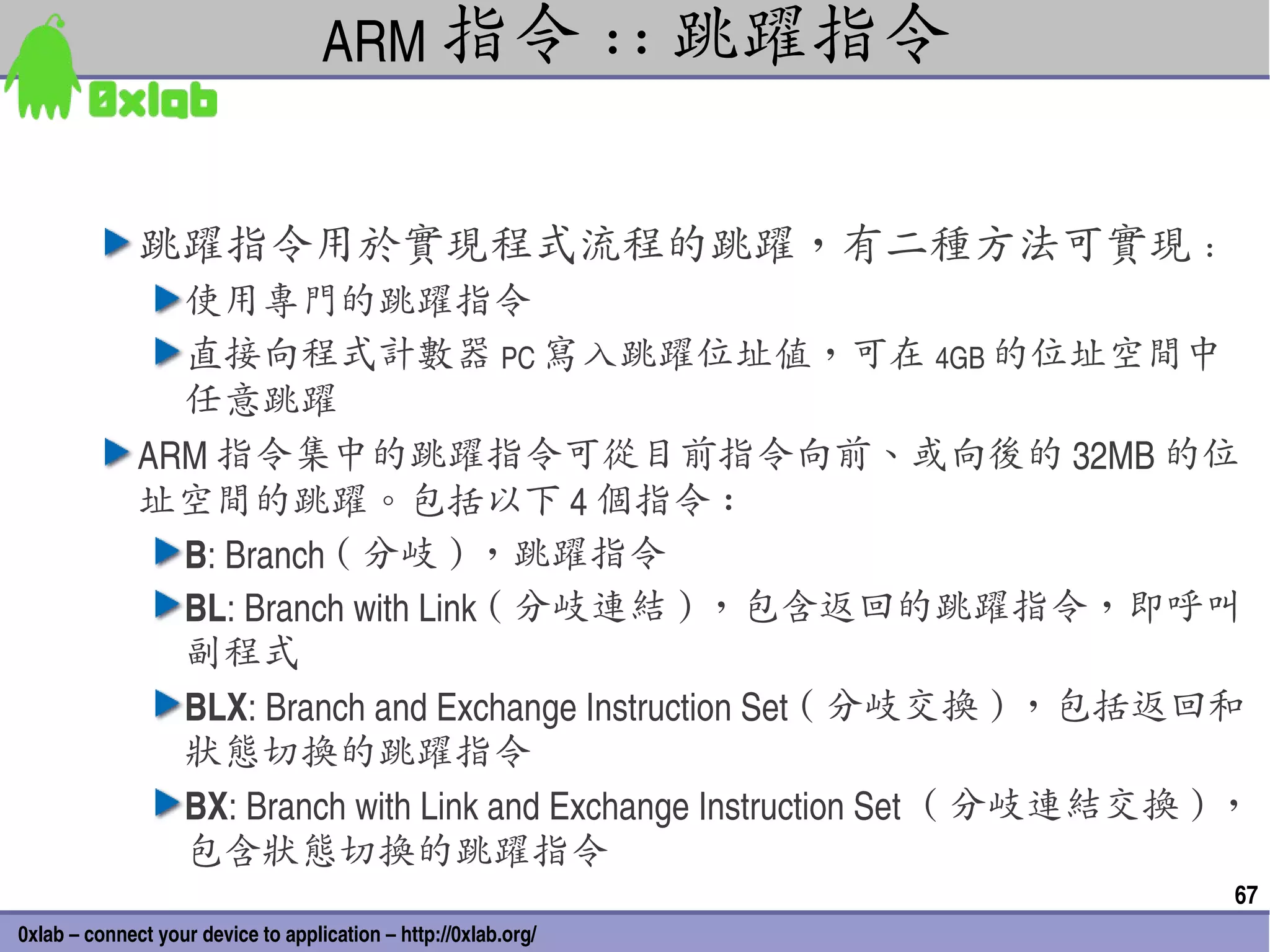
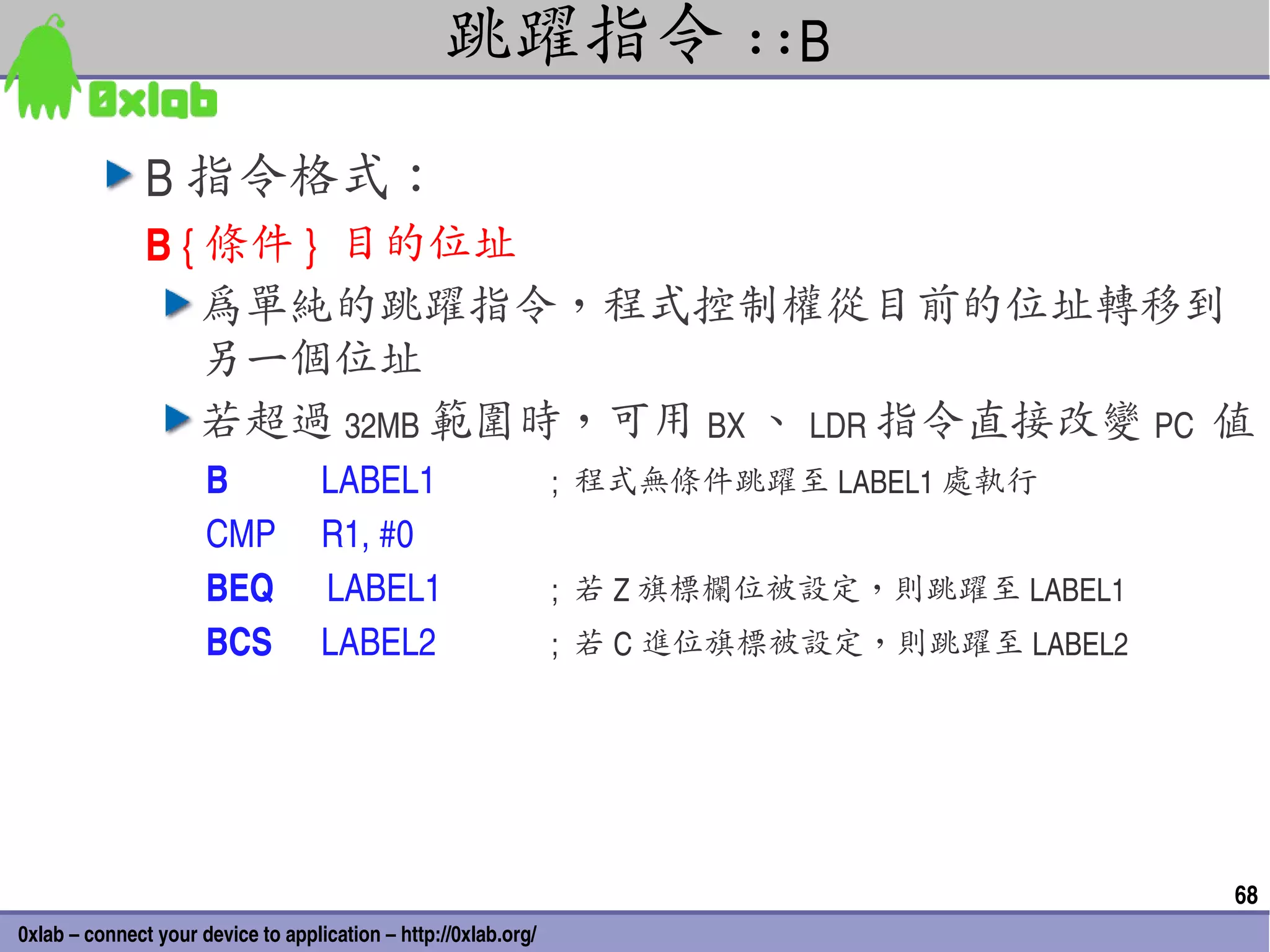
跳躍指令
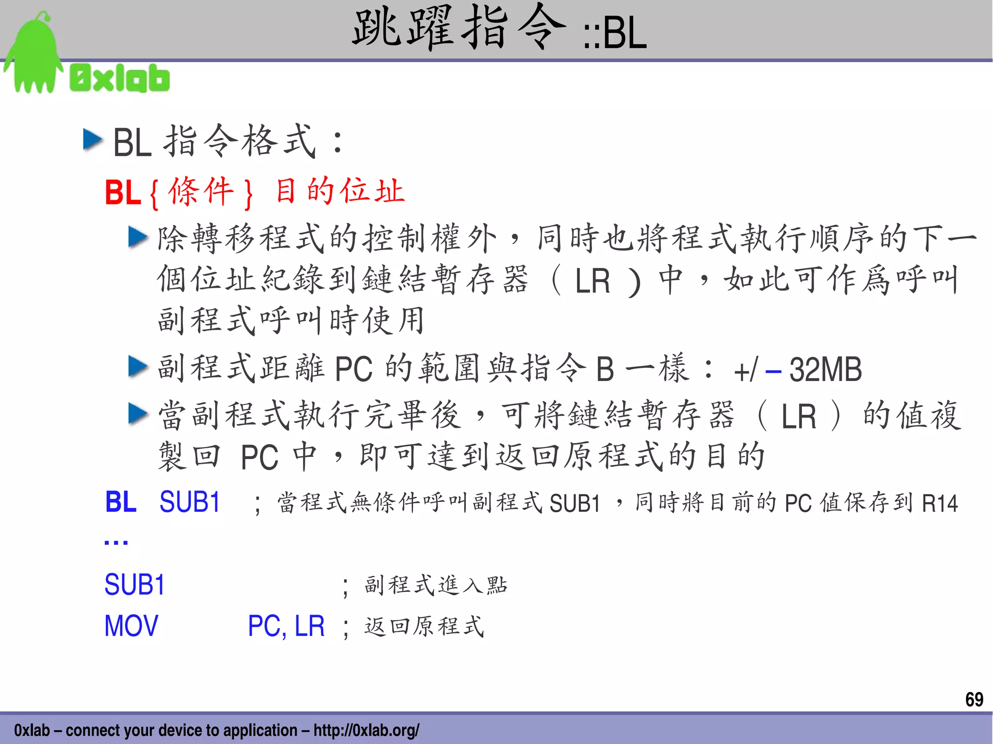
資料處理指令
程式狀態暫存器 (PSR) 處理指令
載入 / 存回指令
協同處理器指令
例外事件產生指令
僅探討 CuRT 所用的指令 47
0xlab – connect your device to application – http://0xlab.org/
48.
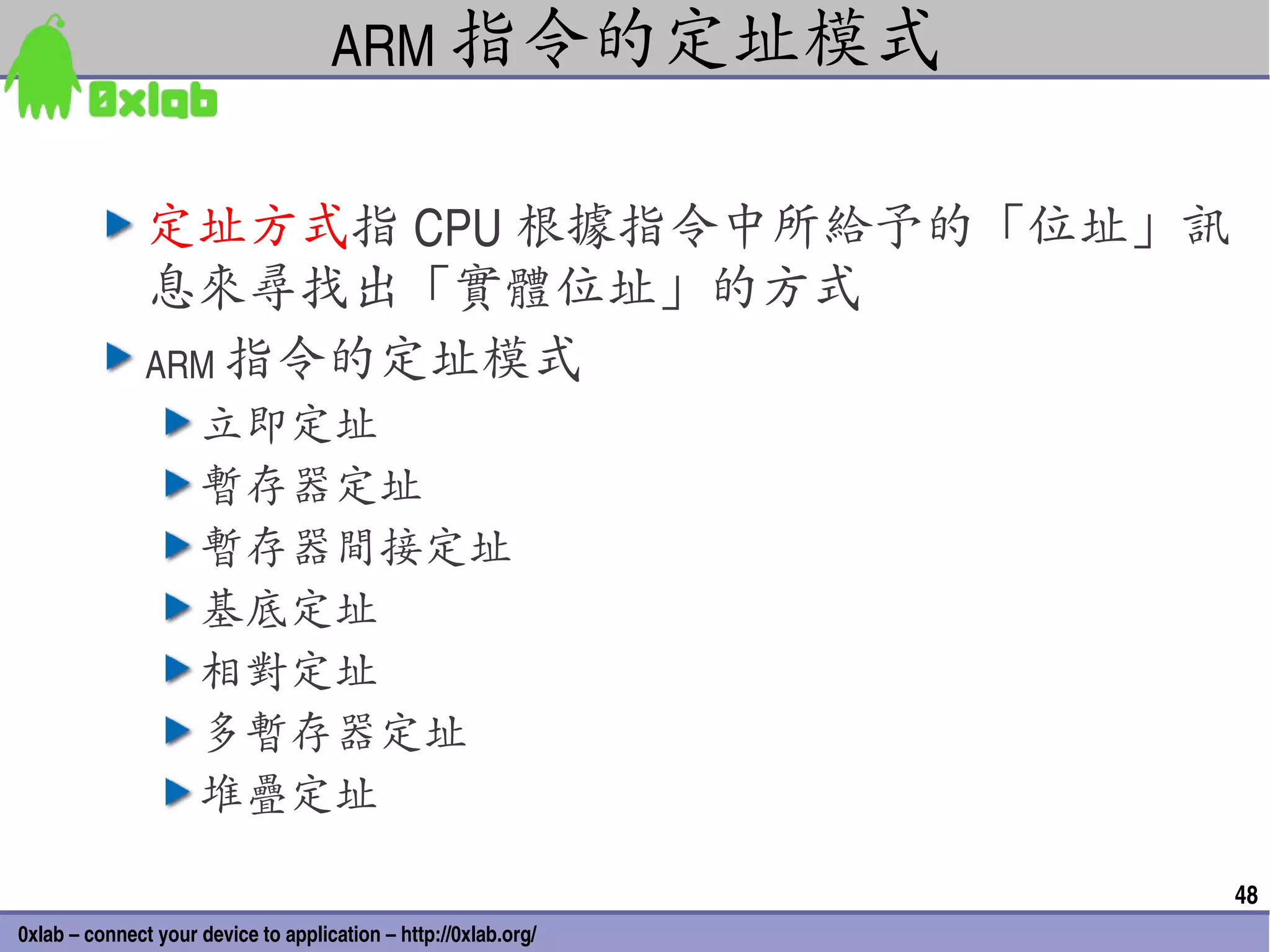
ARM 指令的定址模式
定址方式指 CPU 根據指令中所給予的「位址」訊
息來尋找出「實體位址」的方式
ARM 指令的定址模式
立即定址
暫存器定址
暫存器間接定址
基底定址
相對定址
多暫存器定址
堆疊定址
48
0xlab – connect your device to application – http://0xlab.org/
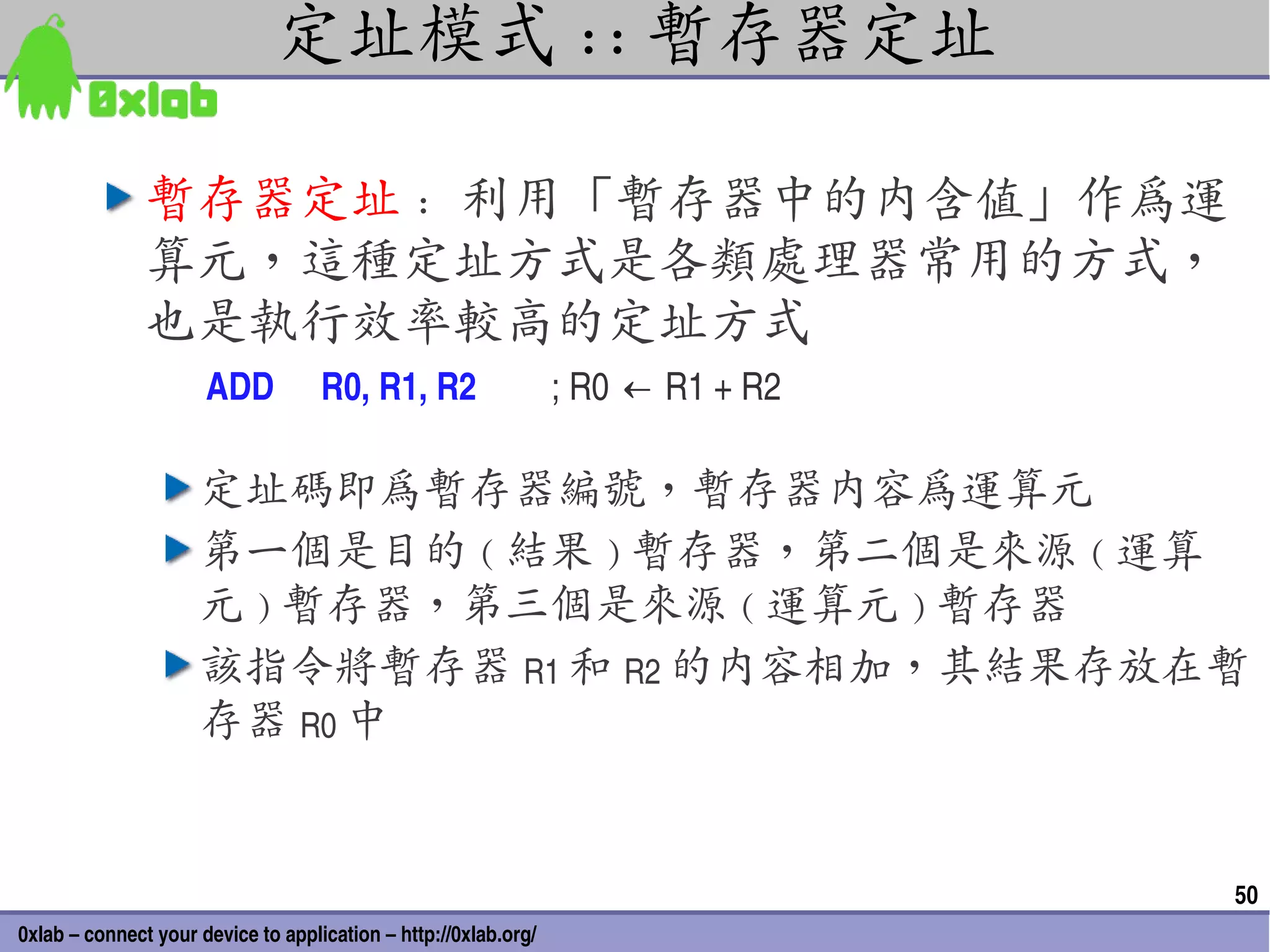
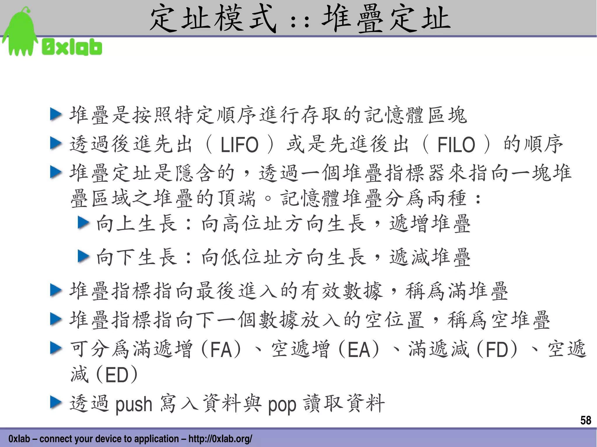
定址模式 :: 堆疊定址
堆疊是按照特定順序進行存取的記憶體區塊
透過後進先出( LIFO )或是先進後出( FILO )的順序
堆疊定址是隱含的,透過一個堆疊指標器來指向一塊堆
疊區域之堆疊的頂端。記憶體堆疊分為兩種 :
向上生長:向高位址方向生長,遞增堆疊
向下生長:向低位址方向生長,遞減堆疊
堆疊指標指向最後進入的有效數據,稱為滿堆疊
堆疊指標指向下一個數據放入的空位置,稱為空堆疊
可分為滿遞增 (FA) 、空遞增 (EA) 、滿遞減 (FD) 、空遞
減 (ED)
透過 push 寫入資料與 pop 讀取資料
58
0xlab – connect your device to application – http://0xlab.org/
59.
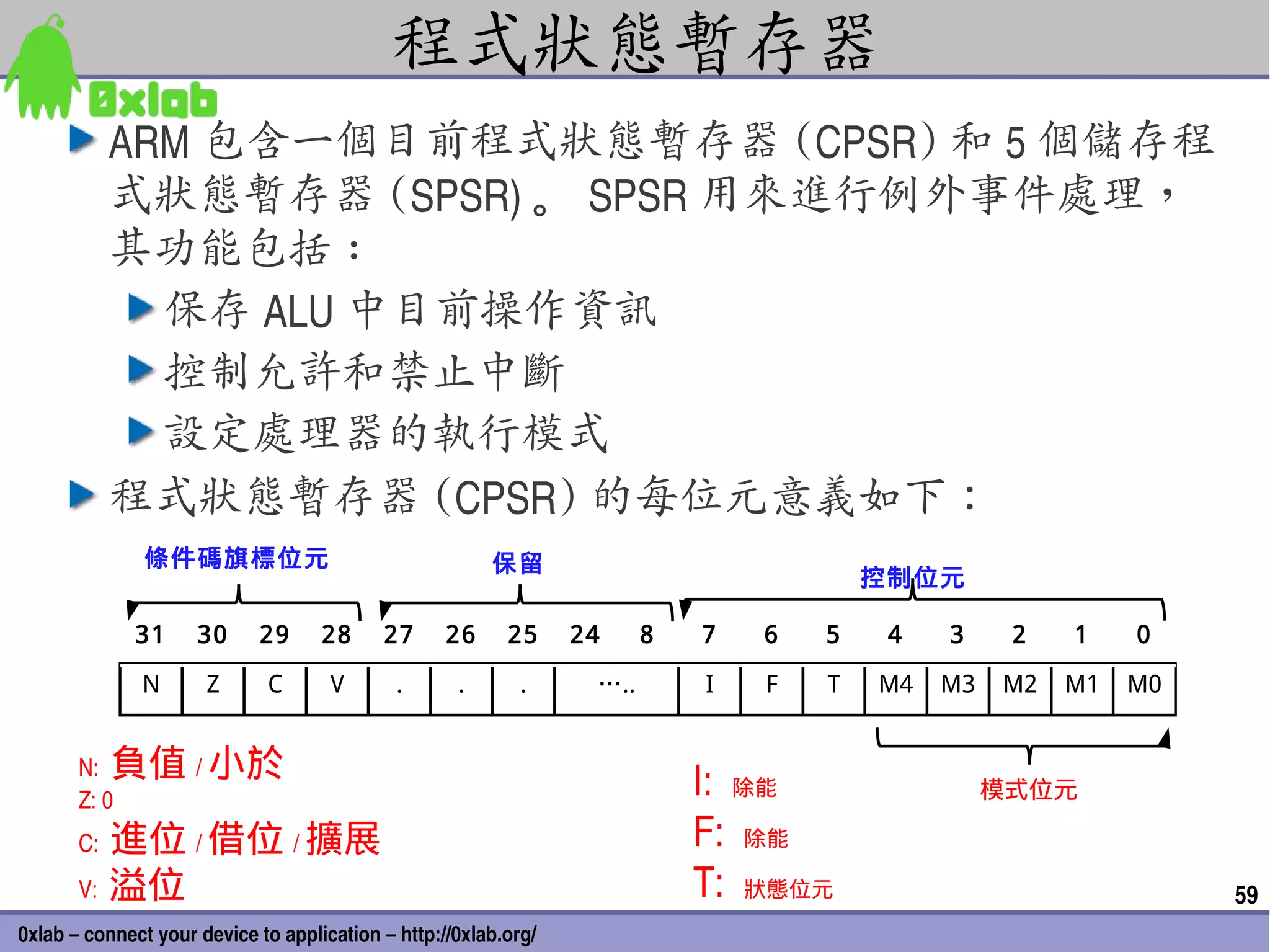
程式狀態暫存器
ARM 包含一個目前程式狀態暫存器 (CPSR) 和 5 個儲存程
式狀態暫存器 (SPSR) 。 SPSR 用來進行例外事件處理,
其功能包括 :
保存 ALU 中目前操作資訊
控制允許和禁止中斷
設定處理器的執行模式
程式狀態暫存器 (CPSR) 的每位元意義如下:
條件碼旗標位元 保留
控制位元
31 30 29 28 27 26 25 24 8 7 6 5 4 3 2 1 0
N Z C V . . . ….. I F T M4 M3 M2 M1 M0
N: 負值 / 小於
Z: 0
I: 除能 模式位元
C: 進位 / 借位 / 擴展 F: 除能
V: 溢位 T: 狀態位元 59
0xlab – connect your device to application – http://0xlab.org/
60.
條件碼旗標欄位 (1/2)
條件碼旗標欄位 (Condition Code Flags)
N 、 Z 、 C 與 V
均為條件碼旗標位元。它們的內
容可被算術或邏輯運算的結果而有所改變,並且
可以決定某條指令是否被執行
在 ARM 狀態下,絕大多數的指令都是有條件執行
在 Thumb 狀態下,僅有跳躍指令都是有條件執行
60
0xlab – connect your device to application – http://0xlab.org/
61.
條件碼旗標欄位 (2/2)
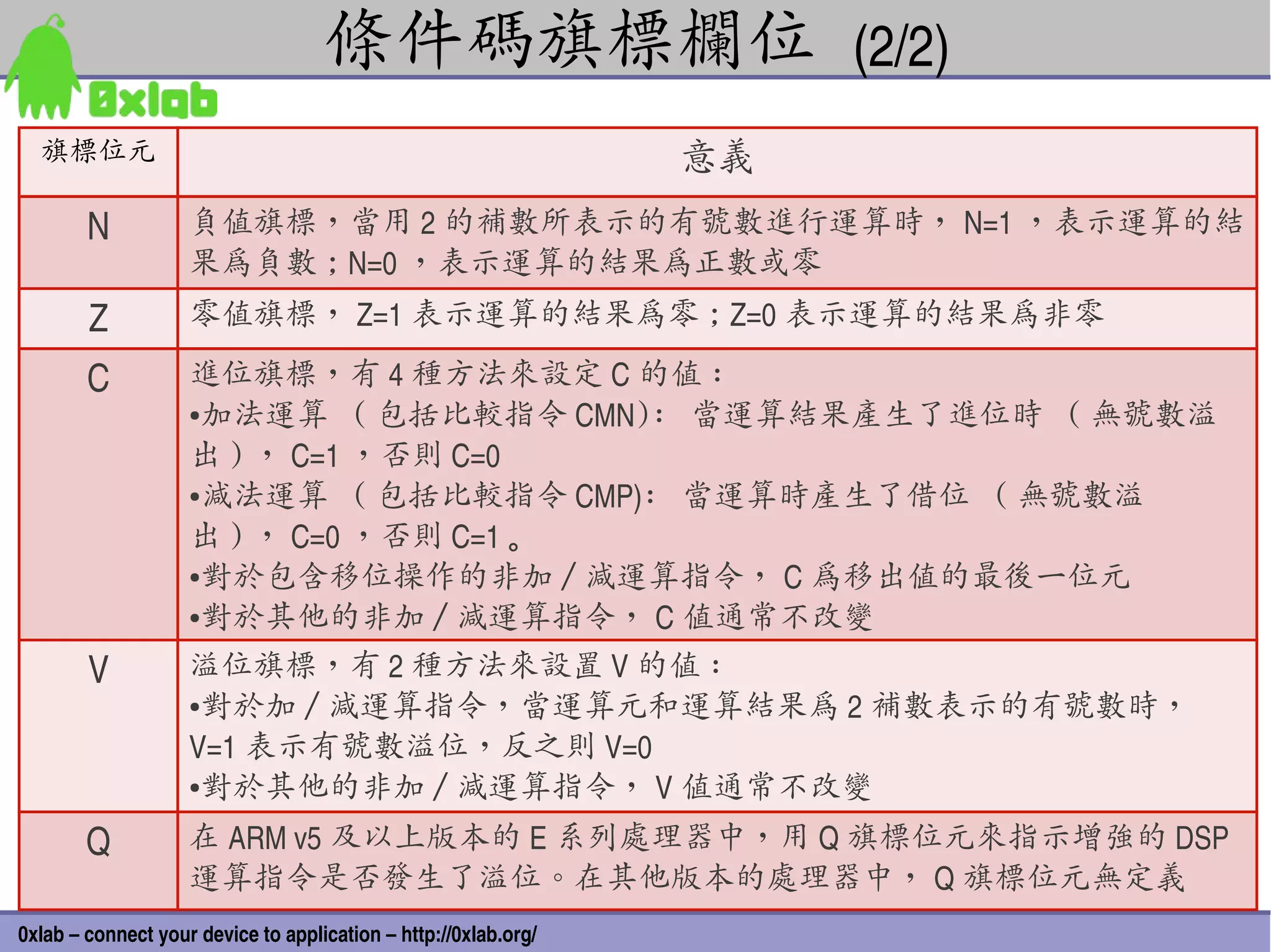
旗標位元 意義
N 負值旗標,當用 2 的補數所表示的有號數進行運算時, N=1 ,表示運算的結
果為負數 ; N=0 ,表示運算的結果為正數或零
Z 零值旗標, Z=1 表示運算的結果為零 ; Z=0 表示運算的結果為非零
C 進位旗標,有 4 種方法來設定 C 的值 :
●加法運算 ( 包括比較指令 CMN): 當運算結果產生了進位時 ( 無號數溢
出 ) , C=1 ,否則 C=0
●減法運算 ( 包括比較指令 CMP): 當運算時產生了借位 ( 無號數溢
出 ) , C=0 ,否則 C=1 。
●對於包含移位操作的非加 / 減運算指令, C 為移出值的最後一位元
●對於其他的非加 / 減運算指令, C 值通常不改變
V 溢位旗標,有 2 種方法來設置 V 的值 :
●對於加 / 減運算指令,當運算元和運算結果為 2 補數表示的有號數時,
V=1 表示有號數溢位,反之則 V=0
●對於其他的非加 / 減運算指令, V 值通常不改變
Q 在 ARM v5 及以上版本的 E 系列處理器中,用 Q 旗標位元來指示增強的 DSP
運算指令是否發生了溢位。在其他版本的處理器中, Q 旗標位元無定義 61
0xlab – connect your device to application – http://0xlab.org/
62.
控制欄位 (1/2)
PSR 的低 8 位元 ( 包括 I 、 F 、 T 和 M[4:0]) 稱之為控制
位元。當發生例外事件時,這些位元可被改變。若處理
器要執行特權模式時,這些位元也可由程式來修改
中斷禁止位元 I 與 F
I =1 ,禁止 IRQ 中斷
F = 1 ,禁止 FIQ 中斷
T 旗標位元 : 該位元反映處理器的執行狀態
T = 0 , ARM 狀態
T = 1 , Thumb 狀態
執行模式位元 M[4:0]: M0 、 M1 、 M2 、 M3 與 M4 是模
式位元。這些位元決定了處理器的執行模式
62
0xlab – connect your device to application – http://0xlab.org/
保留位元
PSR 中的其餘位元為保留位元,當改變 PSR 中的條
件碼旗標位元或控制位元時,保留位元不能被改
變,在程式中也不要用保留位元來儲存資料
這些保留位元將應用於未來 ARM 版本
64
0xlab – connect your device to application – http://0xlab.org/
Part II 回顧
ARM 中斷
ARM 例外處理
ARM 組合語言概況
91
0xlab – connect your device to application – http://0xlab.org/
92.
參考資訊
ARM Limited ARM Architecture Reference Manual, Addison
Wesley, June 2000
ARM Architecture Manual
The ARM Instruction Set – ARM University Program
Steve Furber ARM SystemOnChip Architecture (2nd edition), Addison Wesley,
March 2000
Intel Xscale Programmers Reference Manual
92
0xlab – connect your device to application – http://0xlab.org/

![PMCR (Power Manager Control Register)
31 30 29 28 27 26 25 24 23 22 21 20 19 18 17 16 15 14 13 12 11 10 9 8 7 6 5 4 3 2 1 0
0000 0000 0000 0000 0000 0000 0000 0000
Reserved
IDAE
[0x 40F0 0000]
通常會伴隨「複合式」的控制 register Memory-mapped 位址
同樣落於 0x4000000-0x4400000 的範圍
PCFR (Power Manager General Configuration Register)
31 30 29 28 27 26 25 24 23 22 21 20 19 18 17 16 15 14 13 12 11 10 9 8 7 6 5 4 3 2 1 0
0000 0000 0000 0000 0000 0000 0000 0000
Reserved FP
FS
OPDE
OPDE [0] 3.6864MHz oscillator power-down enable. [0x 40F0 001C]
FP [1] Float PCMCIA controls during Sleep Mode.
FS [2] Float Static Chip Selects during Sleep Mode.
11
Memory-mapped 位址
0xlab – connect your device to application – http://0xlab.org/](https://image.slidesharecdn.com/arm-and-soc-traning-part-ii-system-111203095349-phpapp01/75/ARM-and-SoC-Traning-Part-II-System-11-2048.jpg)
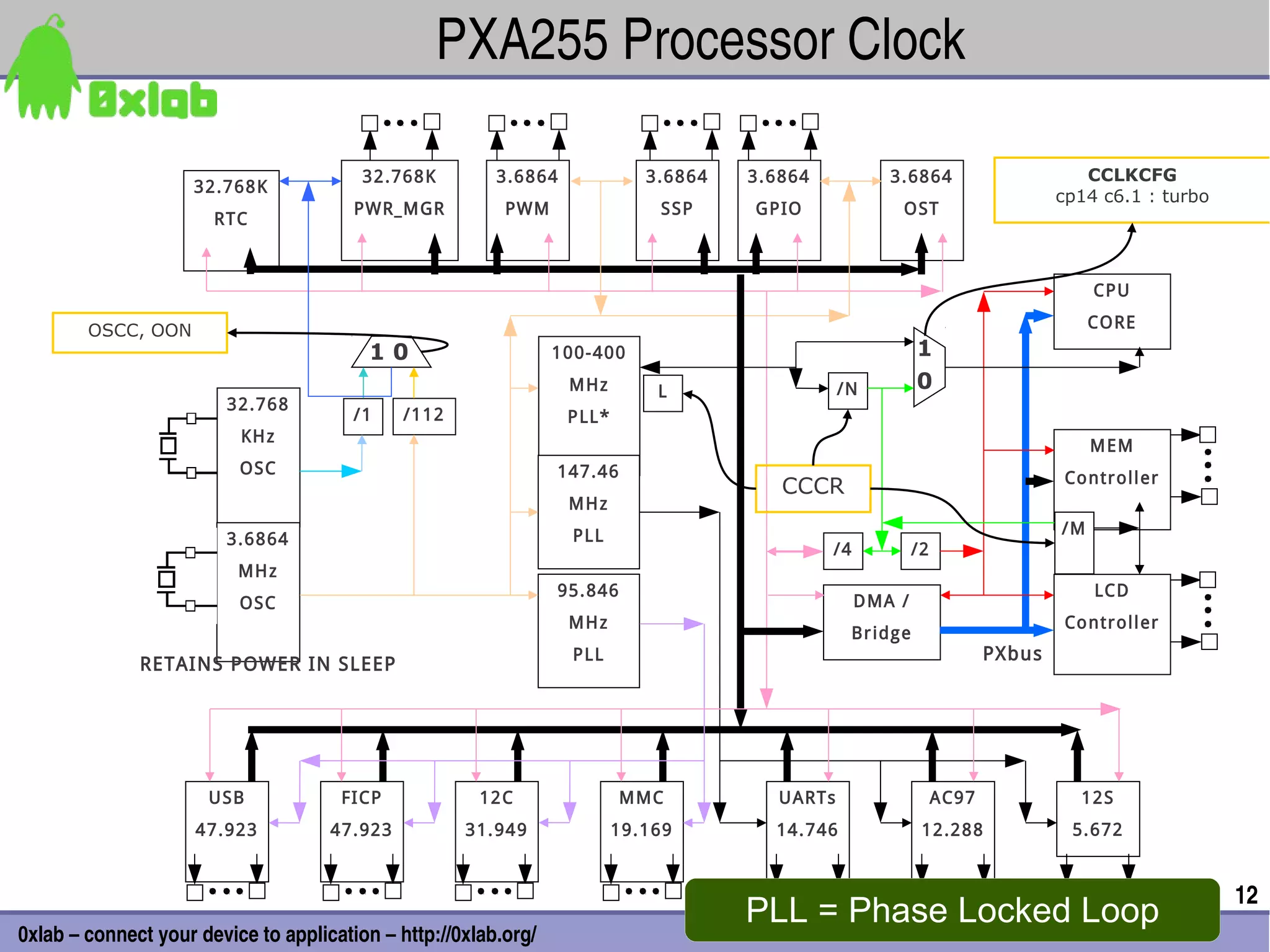
![Core PLL Output Frequencies
Turbo Mode Frequency (MHz) for Values “N” and
Core Clock Configuration Register (CCCR[15:0]) PXbus MEM, LCD SDRAM
L M Programming for Values of “N”: Frequency Frequency max Freq
1.00 1.50 2.00 3.00 (MHz)
(Run)
99.5 ㅡ 199.1 298.6 50 99.5 99.5
27 1
@1.0 V @1.0 V @1.1 v
36 1 132.7 ㅡ ㅡ ㅡ 66 132.7 66
@1.0 V
199.1 298.6 398.1 ㅡ 99.5 99.5 99.5
27 2
@1.0 V @1.1 v @1.3 V
265.4 ㅡ ㅡ ㅡ 132.7 132.7 66
36 2
@1.1 V
331.8 ㅡ ㅡ ㅡ
45 2 165.9 165.9 83
@1.3 V
27 4 398.1 ㅡ ㅡ 196 99.5 99.5
@1.3 V
CCCR (Core Clock Configuration Register)
31 30 29 28 27 26 25 24 23 22 21 20 19 18 17 16 15 14 13 12 11 10 9 8 7 6 5 4 3 2 1 0
0000 0000 0000 0000 0000 0001 0010 0001
Reserved N M L
13
0xlab – connect your device to application – http://0xlab.org/](https://image.slidesharecdn.com/arm-and-soc-traning-part-ii-system-111203095349-phpapp01/75/ARM-and-SoC-Traning-Part-II-System-13-2048.jpg)
![CuRT_v1/arch/arm/mach-pxa/start.S
CuRT_v1/arch/arm/mach-pxa/start.S
init_clock_reg:
init_clock_reg: /* PXA250 Clock Register initialization */
/* PXA250 Clock Register initialization */
ldr r1, =CLK_BASE /* base of clock registers */
ldr r1, =CLK_BASE /* base of clock registers */
ldr r2, =0x00000241
ldr r2, =0x00000241 /* memory clock: 100MHz,
/* memory clock: 100MHz,
normal core clock: 200MHz,
normal core clock: 200MHz,
turbo mode: 400MHz */
turbo mode: 400MHz */
str r2, [r1, #CLK_CCCR]
str r2, [r1, #CLK_CCCR]
CCCR (Core Clock Configuration Register)
31 30 29 28 27 26 25 24 23 22 21 20 19 18 17 16 15 14 13 12 11 10 9 8 7 6 5 4 3 2 1 0
0000 0000 0000 0000 0000 0001 0010 0001
Reserved N M L
N[9:7] Run Mode Frequency : Turbo Mode Frequency
Turbo Mode Freq. = Run Mode Frequency * N
000 , 001 , 101 , 111 – Reserved
001 (Multiplier) = 1
011 (Multiplier) = 1.5
100 (Multiplier) = 2
110 (Multiplier) = 3
☞ Turbo Mode Freq(398.1MHz) = Run Mode Freq(199.1MHz) * N(2)
Address : 0x41300000 14
0xlab – connect your device to application – http://0xlab.org/](https://image.slidesharecdn.com/arm-and-soc-traning-part-ii-system-111203095349-phpapp01/75/ARM-and-SoC-Traning-Part-II-System-14-2048.jpg)
![CuRT_v1/arch/arm/mach-pxa/start.S
CuRT_v1/arch/arm/mach-pxa/start.S
init_clock_reg:
init_clock_reg: /* PXA250 Clock Register initialization */
/* PXA250 Clock Register initialization */
ldr r1, =CLK_BASE /* base of clock registers */
ldr r1, =CLK_BASE /* base of clock registers */
ldr r2, =0x00000241
ldr r2, =0x00000241 /* memory clock: 100MHz,
/* memory clock: 100MHz,
normal core clock: 200MHz,
normal core clock: 200MHz,
turbo mode: 400MHz */
turbo mode: 400MHz */
str r2, [r1, #CLK_CCCR]
str r2, [r1, #CLK_CCCR]
CCCR (Core Clock Configuration Register)
31 30 29 28 27 26 25 24 23 22 21 20 19 18 17 16 15 14 13 12 11 10 9 8 7 6 5 4 3 2 1 0
0000 0000 0000 0000 0000 0001 0010 0001
Reserved N M L
CuRT_v1/includes/arch/arm/mach-pxa/pxa255.h
CuRT_v1/includes/arch/arm/mach-pxa/pxa255.h
/** Clocks Manager */
/** Clocks Manager */
#define CLK_BASE 0x41300000
#define CLK_BASE 0x41300000
#define CLK_REG(_x_)
#define CLK_REG(_x_) *(vulong *)(CLK_BASE + _x_)
*(vulong *)(CLK_BASE + _x_)
#define CLK_CCCR 0x00
#define CLK_CCCR 0x00 /* Core Clock Configuration
/* Core Clock Configuration Register */
Register */
#define CLK_CKEN 0x04
#define CLK_CKEN 0x04 /* Clock Enable Register */
/* Clock Enable Register */
#define CLK_OSCC 0x08
#define CLK_OSCC 0x08 /* Oscillator Configuration
/* Oscillator Configuration Register
Register 15
0xlab – connect your device to application – http://0xlab.org/](https://image.slidesharecdn.com/arm-and-soc-traning-part-ii-system-111203095349-phpapp01/75/ARM-and-SoC-Traning-Part-II-System-15-2048.jpg)
![CCCR (Core Clock Configuration Register)
31 30 29 28 27 26 25 24 23 22 21 20 19 18 17 16 15 14 13 12 11 10 9 8 7 6 5 4 3 2 1 0
0000 0000 0000 0000 0000 0001 0010 0001
Reserved N M L
M [6:5] Memory Frequency :Run Mode Frequency
Memory Freq = Crystal Frequency * L
00 , 11 – Reserved
01(Multiplier) = 1
10(Multiplier) = 2
☞ Memory Freq(99.5MHz) = Crystal Frequency(3.6864MHz) * L(27)
L[4:0] Crystal Frequency: Memory Frequency (3.6864MHz Crystal)
00000 , 00110 to 11111 – Reserved
00001(Multiplier) = 27 (Memory Freq: 99.53MHz)
00010(Multiplier) = 32 (Memory Freq: 117.96MHz)
00011(Multiplier) = 36 (Memory Freq: 132.71MHz)
00100(Multiplier) = 40 (Memory Freq: 147.46MHz)
00101(Multiplier) = 45 (Memory Freq: 165.89MHz)
16
0xlab – connect your device to application – http://0xlab.org/](https://image.slidesharecdn.com/arm-and-soc-traning-part-ii-system-111203095349-phpapp01/75/ARM-and-SoC-Traning-Part-II-System-16-2048.jpg)
![GPIO (General Purpose I/O)
Modem control signals for UART (CTS, RTS, CD, etc) implemented via
GPIO signals
GPIO[58:73] = dual panel color or 16 bit parallel input on LCD
GPIO[23:27] = SPI if both synchronous serial protocols
are required in a single system
Memory
Controller
RTC
O S T ime r
PWM(2) 0x4400_0000 PCMCIA
Inter rupt
& CF XCVR
Contro ller Control
Clo ck & Socket 0, 1
Power Ma n. System Bus
Dynamic SDRAM/
I2S Memory SMROM
I2C Control 4 banks
AC97 Megacell Write Read
FF_U AR T Core B uffe r Buffer
BT_ U ART Variable
Load/Store Data Latency
S low lrD A I/O ASIC
s u B l ar e h p r e P
Dcache Addr
Fast lrD A DMMU (32 Kbytes)
Control
XScale
/ I es o pr u P l ar e n e G
Minicache
i
S SP CS
Core #3,4,5
na r el l ort n o C A MD
NSS P Icache PC
IMMU (32 Kbytes) Static ROM/
U SB Memory Flash
Client Instructions Control SRAM
4 banks
MMC 3.6864 MHz 32.768 KHz
Osc Osc CS #0,1,2
17
0xlab – connect your device to application – http://0xlab.org/](https://image.slidesharecdn.com/arm-and-soc-traning-part-ii-system-111203095349-phpapp01/75/ARM-and-SoC-Traning-Part-II-System-17-2048.jpg)
![CuRT_v1/arch/arm/mach-pxa/start.S
CuRT_v1/arch/arm/mach-pxa/start.S
init_gpio:
init_gpio:
// FFUART
// FFUART
ldr r12, =FFUART_BASE
ldr r12, =FFUART_BASE
ldr
ldr r0,
r0, =0x00000000
=0x00000000
str
str r0,
r0, [r12, #FFLCR]
[r12, #FFLCR]
…
…
//
// First set the output values to a safe/disabled state
First set the output values to a safe/disabled state
//
// before we change any GPIO's outputs start by settings
before we change any GPIO's outputs start by settings
//
// all of them high which is the safest for most signals
all of them high which is the safest for most signals
ldr r12, =GPIO_BASE
ldr r12, =GPIO_BASE
ldr
ldr r0,
r0, =0xffffffff
=0xffffffff
str
str r0,
r0, [r12, #GPIO_GPSR0]
[r12, #GPIO_GPSR0]
str
str r0,
r0, [r12, #GPIO_GPSR1]
[r12, #GPIO_GPSR1]
str
str r0,
r0, [r12, #GPIO_GPSR2]
[r12, #GPIO_GPSR2]
CuRT_v1/includes/arch/arm/mach-pxa/pxa255.h
CuRT_v1/includes/arch/arm/mach-pxa/pxa255.h
/** General Programmable I/O */
/** General Programmable I/O */
#define GPIO_BASE0x40E00000
#define GPIO_BASE0x40E00000
#define GPIO_REG(_x_) *(volatile unsigned long *)(GPIO_BASE + _x_)
#define GPIO_REG(_x_) *(volatile unsigned long *)(GPIO_BASE + _x_)
#define GPIO_GPLR0
#define GPIO_GPLR0 0x00 /* GPIO<31: 0>
0x00 /* GPIO<31: 0> status register */
status register */ 20
#define GPIO_GPLR1
#define GPIO_GPLR1 0x04 /* GPIO<63:32>
0x04 /* GPIO<63:32> status register */
status register */
0xlab – connect your device to application – http://0xlab.org/
#define GPIO_GPLR2
#define GPIO_GPLR2 0x08 /* GPIO<80:64>
0x08 /* GPIO<80:64> status register */
status register */](https://image.slidesharecdn.com/arm-and-soc-traning-part-ii-system-111203095349-phpapp01/75/ARM-and-SoC-Traning-Part-II-System-20-2048.jpg)
![Register Register
GPIO[15:0] GPIO[31:16] GPIO[47:32] GPIO[63:48] GPIO[79:64] GPIO[80]
Type Function
GPLR Monitor Pin State GPLR0 GPLR1 GPLR2
GPSR GPSR0 GPSR1 GPSR2
Control Output
Pin State
GPCR GPCR0 GPCR1 GPCR2
GPDR Set Pin Direction GPDR0 GPDR1 GPDR2
GRER GRER0 GRER1 GRER2
Detect Rising/
Falling Edge
GFER GFER0 GFER1 GFER2
GEDR Detect Edge Type GEDR0 GEDR1 GEDR2
Set Alternate
GAFR GAFR0_L GAFR0_U GAFR1_L GAFR1_U GAFR2_L GAFR2_U
Functions
21
0xlab – connect your device to application – http://0xlab.org/](https://image.slidesharecdn.com/arm-and-soc-traning-part-ii-system-111203095349-phpapp01/75/ARM-and-SoC-Traning-Part-II-System-21-2048.jpg)
![IRQ 與 FIQ
• Program Status Register
31 30 29 28 27 … 8 7 6 5 4 3 2 1 0
N Z C V I F M4 M3 M2 M1 M0
– 若要抑制 interrupts ,將 "F” 或“ I” bit 設定為 1
• 一旦 interrupt 觸發,處理器將變更至 FIQ32_mode registers 或
IRQ32_mode registers
• Switch register banks
• Copies CPSR to SPSR_mode (saves mode, interrupt flags, etc.)
• Changes the CPSR mode bits (M[4:0])
• Disables interrupts
• Copies PC to R14_mode (to provide return address)
• Sets the PC to the vector address of the exception handler
30
0xlab – connect your device to application – http://0xlab.org/](https://image.slidesharecdn.com/arm-and-soc-traning-part-ii-system-111203095349-phpapp01/75/ARM-and-SoC-Traning-Part-II-System-30-2048.jpg)
![CuRT_v1/arch/arm/mach-pxa/arm_port.S
CuRT_v1/arch/arm/mach-pxa/arm_port.S
irq_service_routine:
irq_service_routine:
msr CPSR_c, #(NO_INT | IRQ32_MODE)
msr CPSR_c, #(NO_INT | IRQ32_MODE)
stmfd sp!, {r1-r3}
stmfd sp!, {r1-r3} // push working registers onto IRQ stack
// push working registers onto IRQ stack
mov r1, sp
mov r1, sp // save IRQ stack pointer
// save IRQ stack pointer
add sp, sp, #12
add sp, sp, #12 // adjust IRQ stack pointer
// adjust IRQ stack pointer
sub r2, lr, #4
sub r2, lr, #4 // adjust pc for return
// adjust pc for return
mrs
mrs r3, SPSR
r3, SPSR // copy SPSR (interrupted thread's CPSR)
// copy SPSR (interrupted thread's CPSR)
msr
msr CPSR_c, #(NO_INT | SVC32_MODE)
CPSR_c, #(NO_INT | SVC32_MODE) // change to SVC mode
// change to SVC mode
// save thread's context onto thread's stack
// save thread's context onto thread's stack
stmfd
stmfd sp!,
sp!, {r2}
{r2} // push thread's return pc
// push thread's return pc
stmfd
stmfd sp!,
sp!, {lr}
{lr} // push thread's LR
// push thread's LR
stmfd
stmfd sp!,
sp!, {r4-r12}
{r4-r12} // push thread's r12-r4
// push thread's r12-r4
ldmfd r1!, {r4-r6}
ldmfd r1!, {r4-r6} // move thread's r1-r3 from IRQ stack to
// move thread's r1-r3 from IRQ stack to
// SVC stack
// SVC stack
stmfd sp!, {r4-r6}
stmfd sp!, {r4-r6}
stmfd sp!, {r0}
stmfd sp!, {r0} // push thread's r0 onto thread's stack
// push thread's r0 onto thread's stack
stmfd sp!, {r3}
stmfd sp!, {r3} // push thread's CPSR(IRQ's SPSR)
// push thread's CPSR(IRQ's SPSR)
bl enter_interrupt • 一旦 interrupt 觸發,處理器將變更至 FIQ32_mode registers 或 IRQ32_mode registers
bl enter_interrupt
... • Switch register banks
...
• Copies CPSR to SPSR_mode (saves mode, interrupt flags, etc.)
• Changes the CPSR mode bits (M[4:0])
• Disables interrupts
• Copies PC to R14_mode (to provide return address)
• Sets the PC to the vector address of the exception handler
31
0xlab – connect your device to application – http://0xlab.org/](https://image.slidesharecdn.com/arm-and-soc-traning-part-ii-system-111203095349-phpapp01/75/ARM-and-SoC-Traning-Part-II-System-31-2048.jpg)
![PXA255 Interrupt controller
Interrupt Controller 0 : IRQ All Other Qualified
Level Register(ICLR) 1 : FIQ interrupt Bits
40D0 0008
23 23
XScale CORE
CCR[DIM]=0 & IDLE mode=‘1’
Interrupt Controller
40D0 0004 Mask Register (ICMR)
FIQ
Interrupt Source Bit
CPSR.6(F)
Interrupt Controller
40D0 0010 Pending Register (ICPR) IRQ
Interrupt Controller
CPSR.7(I)
IRQ Pending Register (ICIP)
40D0 0000
Interrupt Controller
40D0 000C FIQ Pending Register (ICFP)
40D0 0014 : Interrupt controller control register (ICCR)
ICCR.0 : disable idle mask(DIM)
39
0xlab – connect your device to application – http://0xlab.org/](https://image.slidesharecdn.com/arm-and-soc-traning-part-ii-system-111203095349-phpapp01/75/ARM-and-SoC-Traning-Part-II-System-39-2048.jpg)
![ICMR (Interrupt Controller Mask Register)
31 30 29 28 27 26 25 24 23 22 21 20 19 18 17 16 15 14 13 12 11 10 9 8 7 6 5 4 3 2 1 0
0000 0000 0000 000? ?000 0000 ???? ????
IM31 – IM28 IM27 – IM24 IM23 – IM20 IM19 – IM17 IM14 – IM12 IM11 – IM8 Reserved
IM[x] Interrupt Mask ‘x’ (where x= 8 through 14 and 17 through 31).
0 – Pending interrupt is masked from becoming active (interrupts are NOT sent to CPU or Power Manager).
1 – Pending interrupt is allowed to become active (interrupts are sent to CPU and Power Manager).
NOTE: In idle mode, the IM bits are ignored if ICCR[DIM] is cleared.
Reserved[07, 15, 16]
Physical Address : 0x40D0/0004
CuRT_v1/arch/arm/mach-pxa/start.S
CuRT_v1/arch/arm/mach-pxa/start.S
/*
/*
* Initializing PXA250 interrupt controller.
* Initializing PXA250 interrupt controller.
*/
*/
mask_off_int_reg: /* Mask off all IRQs and FIQs */
mask_off_int_reg: /* Mask off all IRQs and FIQs */
ldr r1, =(INT_BASE | INT_ICMR)
ldr r1, =(INT_BASE | INT_ICMR)
ldr r2, =0x0 /* interrupt gets mask off */
ldr r2, =0x0 /* interrupt gets mask off */
str r2, [r1]
str r2, [r1] 40
0xlab – connect your device to application – http://0xlab.org/](https://image.slidesharecdn.com/arm-and-soc-traning-part-ii-system-111203095349-phpapp01/75/ARM-and-SoC-Traning-Part-II-System-40-2048.jpg)
![ICLR (Interrupt Controller Level Register)
31 30 29 28 27 26 25 24 23 22 21 20 19 18 17 16 15 14 13 12 11 10 9 8 7 6 5 4 3 2 1 0
0000 0000 0000 000# #000 0000 #### ####
IL31 – IL28 IL27 – IL24 IL23 – IL20 IL19 – IL17 IL14 – IL12 IL11 – IL8 Reserved
IL[x] Interrupt Level ‘x’ (where n = 8 through 14 and 17 through 31).
0 – Interrupt routed to IRQ interrupt input.
1 – Interrupt routed to FIQ interrupt input.
Reserved[07, 15, 16]
Physical Address : 0x40D0/0008
CuRT_v1/arch/arm/mach-pxa/port.c
CuRT_v1/arch/arm/mach-pxa/port.c
void init_os_timer()
void init_os_timer()
{{
INT_REG(INT_ICLR) &= ~BIT26;
INT_REG(INT_ICLR) &= ~BIT26;
TMR_REG(TMR_OSMR0) = PXA255_TMR_CLK / OS_TICKS_PER_SEC;
TMR_REG(TMR_OSMR0) = PXA255_TMR_CLK / OS_TICKS_PER_SEC;
TMR_REG(TMR_OSMR1) = 0x3FFFFFFF;
TMR_REG(TMR_OSMR1) = 0x3FFFFFFF;
TMR_REG(TMR_OSMR2) = 0x7FFFFFFF;
TMR_REG(TMR_OSMR2) = 0x7FFFFFFF;
TMR_REG(TMR_OSMR3) = 0xBFFFFFFF;
TMR_REG(TMR_OSMR3) = 0xBFFFFFFF;
TMR_REG(TMR_OSCR) = 0x00;
TMR_REG(TMR_OSCR) = 0x00;
TMR_REG(TMR_OSSR) = BIT0;
TMR_REG(TMR_OSSR) = BIT0;
TMR_REG(TMR_OIER) = BIT0;
TMR_REG(TMR_OIER) = BIT0;
INT_REG(INT_ICMR) |= BIT26;
INT_REG(INT_ICMR) |= BIT26; 41
}}
0xlab – connect your device to application – http://0xlab.org/](https://image.slidesharecdn.com/arm-and-soc-traning-part-ii-system-111203095349-phpapp01/75/ARM-and-SoC-Traning-Part-II-System-41-2048.jpg)
![ICIP (Interrupt Controller IRQ Pending Register)
31 30 29 28 27 26 25 24 23 22 21 20 19 18 17 16 15 14 13 12 11 10 9 8 7 6 5 4 3 2 1 0
0000 0000 0000 000? ?000 0000 ???? ????
IP31 – IP28 IP27 – IP24 IP23 – IP20 IP19 – IP17 IP14 – IP12 IP11 – IP8 Reserved
IP[x] : IRQ Pending x (where x = 8 through 14 and 17 through 31).
0 – IRQ NOT requested by any enabled source.
1 – IRQ requested by an enabled source.
Reserved[07, 15, 16]
Physical Address : 0x40D0/0000
CuRT_v1/arch/arm/mach-pxa/port.c
CuRT_v1/arch/arm/mach-pxa/port.c
void interrupt_handler()
void interrupt_handler()
{
{
if (INT_REG(INT_ICIP) & BIT26) {
if (INT_REG(INT_ICIP) & BIT26) {
TMR_REG(TMR_OSCR) = 0x00;
TMR_REG(TMR_OSCR) = 0x00;
advance_time_tick();
advance_time_tick();
TMR_REG(TMR_OSSR) = BIT0;
TMR_REG(TMR_OSSR) = BIT0;
}
}
}
}
42
0xlab – connect your device to application – http://0xlab.org/](https://image.slidesharecdn.com/arm-and-soc-traning-part-ii-system-111203095349-phpapp01/75/ARM-and-SoC-Traning-Part-II-System-42-2048.jpg)
![定址模式 :: 立即定址
立即定址 : 運算元本身就在指令中直接加以設
定,只要取出指令也就取到的運算元
ADD R3, R3, #1 ; R3 ← R3+1
將 R3 暫存器的內容加 1 ,結果放回 R3 中
ADD R8, R7, #&ff ; R8 ← R7[7:0]
將 32bit 的 R7 取其低 8bit 的數值,即作 AND 邏輯運算,然後
將結果傳至 R8 中
第二個來源運算元即為立即數值,並要求以「 # 」為
首碼
對於十六進制表示的立即數值,在 「 # 」後加上
「 0x 」 或 「 & 」
49
0xlab – connect your device to application – http://0xlab.org/](https://image.slidesharecdn.com/arm-and-soc-traning-part-ii-system-111203095349-phpapp01/75/ARM-and-SoC-Traning-Part-II-System-49-2048.jpg)
![定址模式 :: 暫存器間接定址
暫存器間接定址 : 以暫存器中的數值作為運算元的位址,而
運算元本身是存放在記憶體中
ADD R0, R1, [R2] ; R0 ← R1+[R2]
以暫存器 R2 的數值作為運算元的位址,在記憶體中取得一個運算元後與 R1 相
加,結果存入暫存器 R0 中
LDR R0, [R1] ; R0 ← [R1]
將 R1 所指向的記憶體單元的內容載入至 R0
STR R0, [R1] ; [R1] ← R0
將 R0 取回至 R1 所指向的記憶體單元中
指令中的定址碼設定一組通用的暫存器編號,被指定的暫存器中存
放運算元的有效位址
運算元則存放在記憶體單元中,暫存器即為位址指標
暫存器間接定址使用一個暫存器(基底暫存器)的數值作為記
憶體的位址
51
0xlab – connect your device to application – http://0xlab.org/](https://image.slidesharecdn.com/arm-and-soc-traning-part-ii-system-111203095349-phpapp01/75/ARM-and-SoC-Traning-Part-II-System-51-2048.jpg)
![定址模式 :: 基底定址 (1/3)
基底定址 : 將暫存器 ( 該暫存器稱之為基底暫存器 ) 的內
容與指令中所給予的位址偏移量加以相加,並進而得到一
個運算元的有效位址
LDR R0, [R1, #4] ; R0 ← [R1+4] ( 前索引定址 )
基底定址是用來處理基底附近的記憶體,包含二種定址:
基底加偏移量:前索引 (PreIndex) 與後索引 (PostIndex) 定址
( 基底 + 索引定址 )
暫存器間接定址則是偏移量為 0 的基底加上偏移定址的方式
但基底加偏移定址中的基底暫存器包含的並非是確定的位址,
基底需加(減)最大 4KB 的偏移來計算出所要處理的位址,也就
是前索引與後索引定址的計算
52
0xlab – connect your device to application – http://0xlab.org/](https://image.slidesharecdn.com/arm-and-soc-traning-part-ii-system-111203095349-phpapp01/75/ARM-and-SoC-Traning-Part-II-System-52-2048.jpg)
![定址模式 :: 基底定址 (2/3)
除找到基底定址所指向的記憶體資料外,還可改
變這基底暫存器
LDR R0, [R1, #4] ! ; R0 ← [R1+4], R1 ← R1+4
改變基底暫存器來指向下一個所傳送的位址,這對於
多筆資料傳送很有用
其中「 ! 」表示指令在完成資料傳送後,同時更新基底
暫存器
ARM 對這種自動索引的方式,不消耗額外的週期
53
0xlab – connect your device to application – http://0xlab.org/](https://image.slidesharecdn.com/arm-and-soc-traning-part-ii-system-111203095349-phpapp01/75/ARM-and-SoC-Traning-Part-II-System-53-2048.jpg)
![定址模式 :: 基底定址 (3/3)
後索引定址 : 基底不包含偏移量來做為傳送的位
址,且再傳送後,自動加上索引的方式
LDR R0, [R1], #4 ; R0 ← [R1], R1 ← R1+4
沒有使用「 ! 」,只用了立即數值的偏移量來作為基底
暫存器的變化量
此外,基底加上索引定址的方式是在指令中指定一個暫
存器為基底,然後再指定另一個暫存器當索引
LDR R0, [R1, R2] ; R0 ← [R1+R2]
54
0xlab – connect your device to application – http://0xlab.org/](https://image.slidesharecdn.com/arm-and-soc-traning-part-ii-system-111203095349-phpapp01/75/ARM-and-SoC-Traning-Part-II-System-54-2048.jpg)
![Preindexed: STR r0, [r1,#12]
Offset r0
Source
12 0x20c 0x5 0x5 Register
for STR
r1
Base
Register 0x200 0x200
Auto-update form: STR r0,[r1,#12]!
Postindexed: STR r0, [r1], #12
Updated r1 Offset
Base 0x20c 12 0x20c
Register r0
Source
Original 0x5 Register
r1
Base for STR
0x200 0x5
Register 0x200
55
0xlab – connect your device to application – http://0xlab.org/](https://image.slidesharecdn.com/arm-and-soc-traning-part-ii-system-111203095349-phpapp01/75/ARM-and-SoC-Traning-Part-II-System-55-2048.jpg)
![定址模式 :: 多暫存器定址
多暫存器定址 : 一道指令可以完成多個暫存器值
的傳送
LDMIA R0, {R1, R2, R3, R4} ; R1 ← [R0]
; R2 ← [R0+4]
; R3 ← [R0+8]
; R4 ← [R0+12]
最多傳送 16 個暫存器
該指令的字尾「 IA 」表示在每次執行完 Load / Store 操
作後, R0 按字元組長度增加,因此,這道指令可將連
續記憶體單元的數值傳送到 R1 ~ R4
57
0xlab – connect your device to application – http://0xlab.org/](https://image.slidesharecdn.com/arm-and-soc-traning-part-ii-system-111203095349-phpapp01/75/ARM-and-SoC-Traning-Part-II-System-57-2048.jpg)
![控制欄位 (1/2)
PSR 的低 8 位元 ( 包括 I 、 F 、 T 和 M[4:0]) 稱之為控制
位元。當發生例外事件時,這些位元可被改變。若處理
器要執行特權模式時,這些位元也可由程式來修改
中斷禁止位元 I 與 F
I =1 ,禁止 IRQ 中斷
F = 1 ,禁止 FIQ 中斷
T 旗標位元 : 該位元反映處理器的執行狀態
T = 0 , ARM 狀態
T = 1 , Thumb 狀態
執行模式位元 M[4:0]: M0 、 M1 、 M2 、 M3 與 M4 是模
式位元。這些位元決定了處理器的執行模式
62
0xlab – connect your device to application – http://0xlab.org/](https://image.slidesharecdn.com/arm-and-soc-traning-part-ii-system-111203095349-phpapp01/75/ARM-and-SoC-Traning-Part-II-System-62-2048.jpg)
![控制欄位 (2/2)
執行模式位元 M[4:0] 的具體定義表
M[4:0] 處理器模式 可存取的暫存器
0b10000 使用者模式 PC, CPSR, R0~R14
0b10001 FIQ 模式 PC, CPSR, SPSR_FIQ, R14_FIQ~R8_FIQ, R7~R0
0b10010 IRQ 模式 PC, CPSR, SPSR_IRQ, R14_IRQ, R13_IRQ, R12~R0
0b10011 管理者模式 PC, CPSR, SPSR_SVC, R14_SVC, R13_SVC, R12~R0
0b10111 終止模式 PC, CPSR, SPSR_ABT, R14_ABT, R13_ABT, R12~R0
0b11011 未定義模式 PC, CPSR, SPSR_UND, R14_UND, R13_UND, R12~R0
0b11111 系統模式 PC, CPSR (ARM v4+), R14~R0
63
0xlab – connect your device to application – http://0xlab.org/](https://image.slidesharecdn.com/arm-and-soc-traning-part-ii-system-111203095349-phpapp01/75/ARM-and-SoC-Traning-Part-II-System-63-2048.jpg)
![跳躍指令 ::BX
BX 指令格式:
BX { 條件 } 目的位址
將暫存器 <Rm> 的數值複製至 PC 中,以達到轉移程式控制權
根據暫存器 <Rm> 的最低位元 <Rm>[0] 來變更指令集狀
態, <Rm>[0] 為 1 ,則變更為 THUMB 指令集狀態。 <Rm>[0] 為
0 ,則變更為 ARM 指令集狀態 ; 其餘 <Rm>[31:1] 移入 PC
此指令可將程式控制權轉移到 4GB 絕對位址的任一位址
CODE 32 ; 從此處起的程式以 ARM 指令集編譯
...
BX R0 ; 若 R0[31:1] 為位址 LABEL1 , R0[0] 為 1 ,
; 當跳躍至 LABEL1 處執行時,切換為 THUMB 指令集狀態
….
CODE 16 ; 指示從此處的程式為 THUMB 指令集狀態
LABEL 1: ; LABEL1 程式進入點
70
0xlab – connect your device to application – http://0xlab.org/](https://image.slidesharecdn.com/arm-and-soc-traning-part-ii-system-111203095349-phpapp01/75/ARM-and-SoC-Traning-Part-II-System-70-2048.jpg)
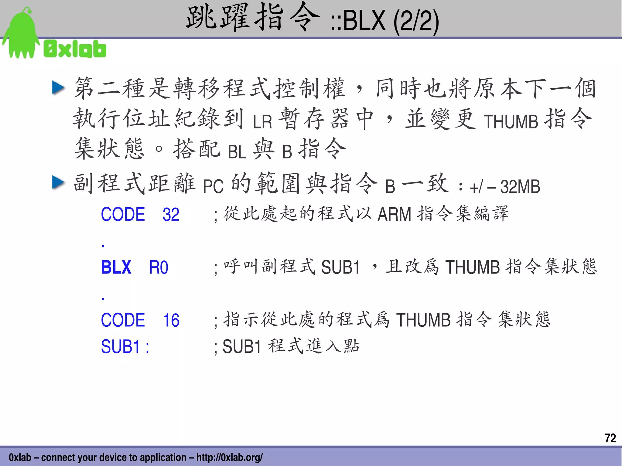
![跳躍指令 :: BLX (1/2)
BLX 指令格式:
BLX 目的位址
從 ARM 指令集跳躍到指令中所指定的目的位址,並將處理
器的工作狀態從 ARM 狀態切換到 THUMB 狀態,該指令同時
將 PC 的目前內容保存到暫存器 R14 中
此指令有兩種使用方式。第一種為與 BX 搭配,可將程式控
制權轉移到 4GB 絕對位址的任一字元位址
CODE 32 ; 從此處起的程式以 ARM 指令集編譯
…
BLX R0 ; 呼叫副程式 SUB1 , R0[0] 為 1 ,切換為 THUMB 指令集狀態
…
CODE 16 ; 指示從此處的程式為 THUMB 指令集狀態
SUB1 : ; SUB1 程式進入點
BX R14
71
0xlab – connect your device to application – http://0xlab.org/](https://image.slidesharecdn.com/arm-and-soc-traning-part-ii-system-111203095349-phpapp01/75/ARM-and-SoC-Traning-Part-II-System-71-2048.jpg)
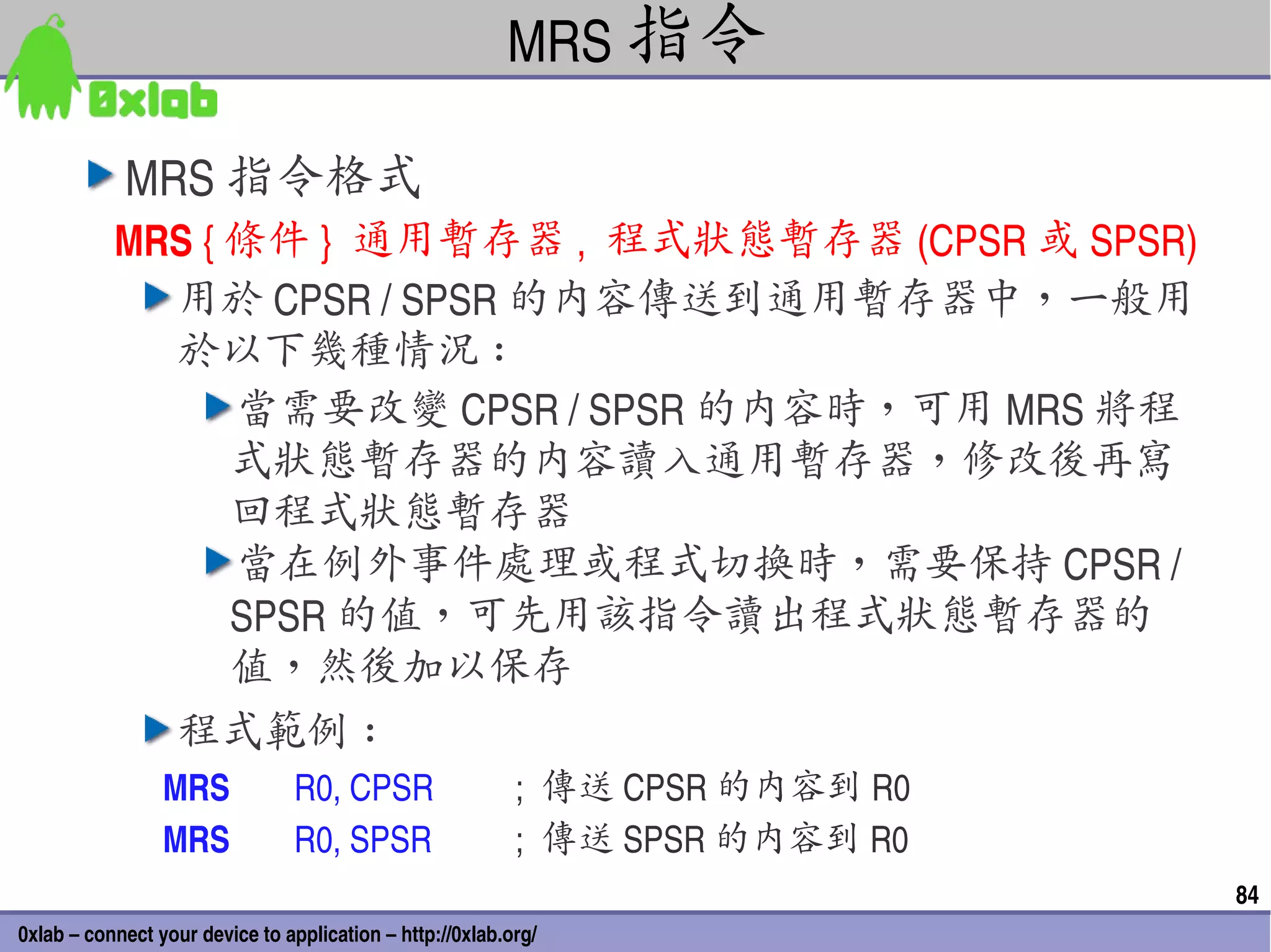
![MSR 指令 (1/3)
MSR 指令的格式
MSR { 條件 } 程式狀態暫存器 (CPSR 或 SPSR) _< 區域 >, 運算元
用於將運算元的內容傳送到 CPSR/SPSR 的特定域中。其中,運算
元可以為通用暫存器或立即數。 < 區域 > 用於設定程式狀態暫存
器中需要操作的位元, 32 位元的程式狀態暫存器可分 4 個區域 :
位元 [31:24] 為條件旗標位元區域,用 f 表示
位元 [23:16] 為狀態位元區域,用 s 表示
位元 [15: 8] 為擴展位元區域,用 x 表示
位元 [ 0: 7] 為控制位元區域,用 c 表示
常用於恢復或改變 CPSR/SPSR 的內容,在使用時,一般要在 MSR
指令中指明要操作的區域
程式範例 :
MSR CPSR, R0 ; 傳送 R0 的內容到 CPSR
MSR SPSR, R0 ; 傳送 R0 的內容到 SPSR
MSR CPSR_c, R0 ; 傳送 R0 的內容到 CPSR
; 但僅修改 CPSR 中的控制位元區域 85
0xlab – connect your device to application – http://0xlab.org/](https://image.slidesharecdn.com/arm-and-soc-traning-part-ii-system-111203095349-phpapp01/75/ARM-and-SoC-Traning-Part-II-System-85-2048.jpg)
![MSR 指令 (2/3)
在使用者模式的指令動作範例:
MSR CPSR_all, Rm ; 傳送 Rm[31:28] 的內容到 CPSR[31:0]
MSR CPSR_flg, Rm ; 傳送 Rm[31:28] 的內容到 CPSR[31:28]
MSR CPSR_flg, #0xA0000000 ; 設定 CPSR[31:28] 為 0xA
; ( 設定 N 、 C; 清除 Z 、 V)
MRS Rd, CPSR ; 傳送 Rm[31:0] 的內容到 CPSR[31:0]
86
0xlab – connect your device to application – http://0xlab.org/](https://image.slidesharecdn.com/arm-and-soc-traning-part-ii-system-111203095349-phpapp01/75/ARM-and-SoC-Traning-Part-II-System-86-2048.jpg)
![MSR 指令 (3/3)
在特權模式的指令動作範例:
MSR CPSR_all, Rm ; 傳送 Rm[31:0] 的內容到 CPSR[31:0]
MSR CPSR_flg, Rm ; 傳送 Rm[31:28] 的內容到 CPSR[31:28]
MSR CPSR_flg, #0x50000000 ; 設定 CPSR[31:28] 為 0x5
; ( 設定 Z 、 V; 清除 N 、 C)
MSR SPSR_all, Rm ; 傳送 Rm[31:0] 的內容到 SPSR[31:0]
MSR SPSR_flg, Rm ; 傳送 Rm[31:28] 的內容到 SPSR[31:28]
MSR SPSR_flg, #0xC0000000 ; 設定 SPSR[31:28] 為 0xC
; ( 設定 N 、 Z; 清除 C 、 V)
MRS Rd, SPSR ; 傳送 Rm[31:0] 的內容到 SPSR[31:0]
87
0xlab – connect your device to application – http://0xlab.org/](https://image.slidesharecdn.com/arm-and-soc-traning-part-ii-system-111203095349-phpapp01/75/ARM-and-SoC-Traning-Part-II-System-87-2048.jpg)
![LDR 指令
LDR 指令格式:
LDR { 條件 } 目的暫存器 , < 記憶體位址>
程式範例
LDR R0, [R1] ; 將記憶體位址為 R1 的字元組資料讀到 R0
LDR R0, [R1, R2] ; 將記憶體位址為 R1+R2 的字元組資料讀到 R0
LDR R0, [R1, #8] ; 將記憶體位址為 R1+8 的字元組資料讀到 R0
LDR R0, [R1, R2] ! ; 將記憶體位址為 R1+R2 的字元組資料讀到 R0 ,
; 並將新位址 R1+R2 寫入 R1
LDR R0, [R1, #8] ! ; 將記憶體位址為 R1+8 的字元組資料讀到 R0 ,
; 並將新位址 R1+8 寫入 R1
LDR R0, [R1], R2 ; 將記憶體位址為 R1 的字元組資料讀到 R0 ,
; 並將新位址 R1+R2 寫入 R1
LDR R0, [R1, R2, LSL #2] ! ; 將記憶體位址為 R1+R2×4 的字元組資料
; 讀到R0 ,並將新位址 R1+R2×4 寫入 R1
LDR R0, [R1], R2, LSL #2 ; 將記憶體位址為 R1 的字元組資料讀到 R0 ,
; 並將新位址 R1+R2×4 寫入 R1 89
0xlab – connect your device to application – http://0xlab.org/](https://image.slidesharecdn.com/arm-and-soc-traning-part-ii-system-111203095349-phpapp01/75/ARM-and-SoC-Traning-Part-II-System-89-2048.jpg)
![STR 指令
STR 指令格式:
STR { 條件 } 來源暫存器 , < 記憶體位址>
程式範例
STR R0, [R1, #8] ; 將 R0 中的字元組資料寫入到
; 以 R1 為位址的記憶體中,並將新位址
; R1+8 寫入 R1
STR R0, [R1, #8] ! ; 將 R0 中的字元組資料寫入到
; 以 R1+8 為位址的記憶體中,並將新位址
; R1+8 寫入 R1
90
0xlab – connect your device to application – http://0xlab.org/](https://image.slidesharecdn.com/arm-and-soc-traning-part-ii-system-111203095349-phpapp01/75/ARM-and-SoC-Traning-Part-II-System-90-2048.jpg)


![[嵌入式系統] MCS-51 實驗 - 使用 IAR (1)](https://cdn.slidesharecdn.com/ss_thumbnails/mcs51iarpart1-150613071712-lva1-app6892-thumbnail.jpg?width=640&height=640&fit=bounds)


