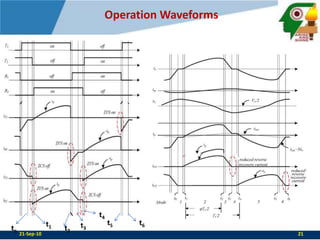
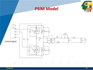
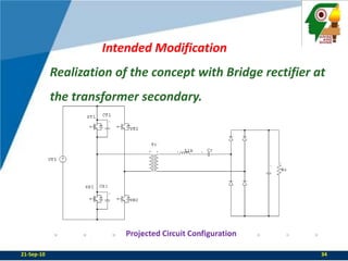
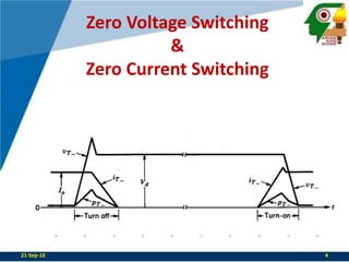
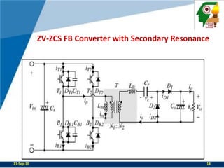
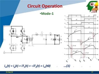
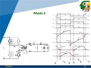
Zero-Voltage- and Zero-Current-Switching with Series Resonance in FB Converter Utilizing Leakage InductancePresented by:Guided By:JoemonRaju Joseph KReg No.- 09HN026M tech PE & DDr. S Suresh Kumar(Professor and Head)Dept. of EEE22-Sep-101
OverviewZVS and ZCSLiteratures on  ZV-ZCSBase Paper Concept & MethodologySimulationSummaryProposed ModificationReferences22-Sep-102
OverviewZVS and ZCSLiteratures on  ZV-ZCSBase Paper Concept & MethodologySimulationSummaryProposed ModificationReferences22-Sep-103
Zero Voltage Switching &Zero Current Switching22-Sep-104
MeritsLossless switching transitionReduced EMI/RFI during switching due to transitionShort circuit tolerationReduction in switching stresses22-Sep-105
OverviewZVS and ZCSLiteratures on  ZV-ZCSBase Paper Concept & MethodologySimulationSummaryProposed ModificationReferences 22-Sep-106
ZCS Circuit MethodologyFig: 1 – Converter with hard switching Auxiliary CircuitFig:2- Fully resonant auxiliary circuitReference [5]22-Sep-107
ZVS Circuit MethodologyFig:3 FB Converter with ZVSReference [13]22-Sep-108
ZV-ZCS Circuit MethodologyUsing Additional Auxillary CircuitsFig:4 FB Converter with Auxiliary Voltage SourceReference [11]22-Sep-109
Using Series Resonant ConvertersFig:5 HB LCL-T ResonantConverterReference [16]1022-Sep-10
Preference for ZV-ZCS Topologies ZCS circuits – Auxiliary circuit Conduction losses, voltage stresses in boost diodeZVS circuits – high circulating losses, high valued inductor with increase in power22-Sep-1011
Choice of IGBTHas lower cost considering high power and high voltage applications .ZVS realizable by  adding additional lossless turn off snubber in parallel22-Sep-1012
OverviewZVS and ZCSLiteratures on  ZV-ZCSBase Paper Concept & MethodologySimulationSummaryProposed ModificationReferences 22-Sep-1013
ZV-ZCS FB Converter with Secondary Resonance22-Sep-1014
ConceptSRC based circuitLeakage inductance of transformer participates in resonanceTurn-on of leading legs possible under all operating conditions and lossless snubber reduces their turn off lossesLagging legs can be turned on at ZV and turned off  near ZC without additional aux. circuits22-Sep-1015
Control SignalNormal PWMPhase Shifted PWM22-Sep-1016
Circuit OperationMode-1im(t) = ip(t) = iT1(t) = −iT2(t) = im(t0)		...(1)22-Sep-1017
Mode-222-Sep-1018
is(t) = sin ωr(t − t1)  x  nVin − (Vo − Vc(t1))/Zo	…(2)ωr = 2πfr = 1/√(LlkCr)	…(angular resonance frequency)Zo = √(Lr/Cr)		…(Characteristic Impedance)im(t) = im(t1) + (Vin/Lm) x (t − t1)		 ….(3)ip(t) = im(t) + nis(t) = iT1(t) = iB2(t)  		....(4)22-Sep-1019
Mode-3is(t) = is (t2) cos ωr(t − t2) − [Vo − Vc(t2)] x sin ωr(t − t2)/Zo …(5)ip(t) = im(t) + nis (t) = −iB1(t) = iB2(t)	     ...(6)21-Sep-1020
Operation Waveformst4t5t6t1t3tot221-Sep-1021
Other Design FactorsFrequency Ratio:		F = fr/fsQuality Factor:		Q =4ωrLlk/Rotch= (CT1+CB1) x Vin/ (Ip1+ Im2max)… Charging time of  					      Capacitance21-Sep-1022
OverviewZVS and ZCSLiteratures on  ZV-ZCSBase Paper Concept & MethodologySimulationSummaryProposed ModificationReferences21-Sep-1023
Assumptions for AnalysisIdeal SwitchesRipple free  Input VoltageIdeal transformer with magnetizing and leakage inductances aloneFrequency ratio, F=122-Sep-1024
PSIM ModelControl Signal21-Sep-1025
Model Parameters21-Sep-1026
Phase Shifted PWM Generation21-Sep-1027
21-Sep-1028
Simulation ResultsPhase Shifted PWM Signals21-Sep-1029
Simulation ResultsSwitching CurrentsZVS ONZVS ONZCS OFF21-Sep-1030
OverviewZVS and ZCSLiteratures on  ZV-ZCSBase Paper Concept & MethodologySummaryProposed ModificationReferences21-Sep-1031
Inference from Literatures: ZV-ZCS has upper hand in effectiveness rather than ZVS or ZCS alone
IGBT is preferable for high power applicationInference from Base Paper:Transformer design plays a crucial role for ZV-ZCS to avoid additional inductor 22-Sep-1032
OverviewZVS and ZCSLiteratures on  ZV-ZCSBase Paper Concept & MethodologyMethodologySummaryProposed ModificationReferences21-Sep-1033
		Intended ModificationRealization of the concept with Bridge rectifier at  the transformer secondary.Projected Circuit Configuration21-Sep-1034
References Eung-Ho Kim and Bong-Hwan Kwon,” Zero-Voltage- and Zero-Current-Switching Full-Bridge Converter With Secondary Resonance”, IEEE Trans. Ind. Electron., vol. 57, no. 3, pp. 1017–1025, Mar. 2010.X. Wu, J. Zhang, X. Ye, and Z. Qian, “Analysis and derivations for a  family ZVS converter based on a new active clamp ZVS cell,” IEEE Trans. Ind. Electron., vol. 55, no. 2, pp. 773–781, Feb. 2008.J. J. Lee, J. M. Kwon, E. H. Kim, and B. H. Kwon, “Dual series resonant active-clamp converter,” IEEE Trans. Ind. Electron., vol. 55, no. 2, pp. 699–710, Feb. 2008.C. M. Wang, “A novel ZCS-PWM flyback converter with a simple ZCSPWM        commutation cell,” IEEE Trans. Ind. Electron., vol. 55, no. 2, pp. 749–757,  Feb. 2008.  X. Wu, X. Xie, C. Zhao, Z. Qian, and R. Zhao, “Low voltage and current stress ZVZCS full bridge DC–DC converter using center tapped rectifier reset,” IEEE Trans. Ind. Electron., vol. 55, no. 3, pp. 1470–1477, Mar. 2008.M. Borage, S. Tiwari, and S. Kotaiah, “LCL-T resonant converter with clamp diodes: A novel constant-current power supply with inherent constant-voltage limit,” IEEE Trans. Ind. Electron., vol. 54, no. 2, pp. 741–746, Apr. 2007.3521-Sep-10

Zero Voltage Zero Current

  • 1.
    Zero-Voltage- and Zero-Current-Switchingwith Series Resonance in FB Converter Utilizing Leakage InductancePresented by:Guided By:JoemonRaju Joseph KReg No.- 09HN026M tech PE & DDr. S Suresh Kumar(Professor and Head)Dept. of EEE22-Sep-101
  • 2.
    OverviewZVS and ZCSLiteratureson ZV-ZCSBase Paper Concept & MethodologySimulationSummaryProposed ModificationReferences22-Sep-102
  • 3.
    OverviewZVS and ZCSLiteratureson ZV-ZCSBase Paper Concept & MethodologySimulationSummaryProposed ModificationReferences22-Sep-103
  • 4.
    Zero Voltage Switching&Zero Current Switching22-Sep-104
  • 5.
    MeritsLossless switching transitionReducedEMI/RFI during switching due to transitionShort circuit tolerationReduction in switching stresses22-Sep-105
  • 6.
    OverviewZVS and ZCSLiteratureson ZV-ZCSBase Paper Concept & MethodologySimulationSummaryProposed ModificationReferences 22-Sep-106
  • 7.
    ZCS Circuit MethodologyFig:1 – Converter with hard switching Auxiliary CircuitFig:2- Fully resonant auxiliary circuitReference [5]22-Sep-107
  • 8.
    ZVS Circuit MethodologyFig:3FB Converter with ZVSReference [13]22-Sep-108
  • 9.
    ZV-ZCS Circuit MethodologyUsingAdditional Auxillary CircuitsFig:4 FB Converter with Auxiliary Voltage SourceReference [11]22-Sep-109
  • 10.
    Using Series ResonantConvertersFig:5 HB LCL-T ResonantConverterReference [16]1022-Sep-10
  • 11.
    Preference for ZV-ZCSTopologies ZCS circuits – Auxiliary circuit Conduction losses, voltage stresses in boost diodeZVS circuits – high circulating losses, high valued inductor with increase in power22-Sep-1011
  • 12.
    Choice of IGBTHaslower cost considering high power and high voltage applications .ZVS realizable by adding additional lossless turn off snubber in parallel22-Sep-1012
  • 13.
    OverviewZVS and ZCSLiteratureson ZV-ZCSBase Paper Concept & MethodologySimulationSummaryProposed ModificationReferences 22-Sep-1013
  • 14.
    ZV-ZCS FB Converterwith Secondary Resonance22-Sep-1014
  • 15.
    ConceptSRC based circuitLeakageinductance of transformer participates in resonanceTurn-on of leading legs possible under all operating conditions and lossless snubber reduces their turn off lossesLagging legs can be turned on at ZV and turned off near ZC without additional aux. circuits22-Sep-1015
  • 16.
    Control SignalNormal PWMPhaseShifted PWM22-Sep-1016
  • 17.
    Circuit OperationMode-1im(t) =ip(t) = iT1(t) = −iT2(t) = im(t0) ...(1)22-Sep-1017
  • 18.
  • 19.
    is(t) = sinωr(t − t1) x nVin − (Vo − Vc(t1))/Zo …(2)ωr = 2πfr = 1/√(LlkCr) …(angular resonance frequency)Zo = √(Lr/Cr) …(Characteristic Impedance)im(t) = im(t1) + (Vin/Lm) x (t − t1) ….(3)ip(t) = im(t) + nis(t) = iT1(t) = iB2(t) ....(4)22-Sep-1019
  • 20.
    Mode-3is(t) = is(t2) cos ωr(t − t2) − [Vo − Vc(t2)] x sin ωr(t − t2)/Zo …(5)ip(t) = im(t) + nis (t) = −iB1(t) = iB2(t) ...(6)21-Sep-1020
  • 21.
  • 22.
    Other Design FactorsFrequencyRatio: F = fr/fsQuality Factor: Q =4ωrLlk/Rotch= (CT1+CB1) x Vin/ (Ip1+ Im2max)… Charging time of Capacitance21-Sep-1022
  • 23.
    OverviewZVS and ZCSLiteratureson ZV-ZCSBase Paper Concept & MethodologySimulationSummaryProposed ModificationReferences21-Sep-1023
  • 24.
    Assumptions for AnalysisIdealSwitchesRipple free Input VoltageIdeal transformer with magnetizing and leakage inductances aloneFrequency ratio, F=122-Sep-1024
  • 25.
  • 26.
  • 27.
    Phase Shifted PWMGeneration21-Sep-1027
  • 28.
  • 29.
    Simulation ResultsPhase ShiftedPWM Signals21-Sep-1029
  • 30.
    Simulation ResultsSwitching CurrentsZVSONZVS ONZCS OFF21-Sep-1030
  • 31.
    OverviewZVS and ZCSLiteratureson ZV-ZCSBase Paper Concept & MethodologySummaryProposed ModificationReferences21-Sep-1031
  • 32.
    Inference from Literatures:ZV-ZCS has upper hand in effectiveness rather than ZVS or ZCS alone
  • 33.
    IGBT is preferablefor high power applicationInference from Base Paper:Transformer design plays a crucial role for ZV-ZCS to avoid additional inductor 22-Sep-1032
  • 34.
    OverviewZVS and ZCSLiteratureson ZV-ZCSBase Paper Concept & MethodologyMethodologySummaryProposed ModificationReferences21-Sep-1033
  • 35.
    Intended ModificationRealization ofthe concept with Bridge rectifier at the transformer secondary.Projected Circuit Configuration21-Sep-1034
  • 36.
    References Eung-Ho Kimand Bong-Hwan Kwon,” Zero-Voltage- and Zero-Current-Switching Full-Bridge Converter With Secondary Resonance”, IEEE Trans. Ind. Electron., vol. 57, no. 3, pp. 1017–1025, Mar. 2010.X. Wu, J. Zhang, X. Ye, and Z. Qian, “Analysis and derivations for a family ZVS converter based on a new active clamp ZVS cell,” IEEE Trans. Ind. Electron., vol. 55, no. 2, pp. 773–781, Feb. 2008.J. J. Lee, J. M. Kwon, E. H. Kim, and B. H. Kwon, “Dual series resonant active-clamp converter,” IEEE Trans. Ind. Electron., vol. 55, no. 2, pp. 699–710, Feb. 2008.C. M. Wang, “A novel ZCS-PWM flyback converter with a simple ZCSPWM commutation cell,” IEEE Trans. Ind. Electron., vol. 55, no. 2, pp. 749–757, Feb. 2008. X. Wu, X. Xie, C. Zhao, Z. Qian, and R. Zhao, “Low voltage and current stress ZVZCS full bridge DC–DC converter using center tapped rectifier reset,” IEEE Trans. Ind. Electron., vol. 55, no. 3, pp. 1470–1477, Mar. 2008.M. Borage, S. Tiwari, and S. Kotaiah, “LCL-T resonant converter with clamp diodes: A novel constant-current power supply with inherent constant-voltage limit,” IEEE Trans. Ind. Electron., vol. 54, no. 2, pp. 741–746, Apr. 2007.3521-Sep-10