SlideShare a Scribd company logo
1 of 29
Download to read offline
DS2438
                                                                       Smart Battery Monitor
www.maxim-ic.com
FEATURES                                                  PIN ASSIGNMENT
                   ®
§   Unique 1-Wire interface requires only one
    port pin for communication                                 GND         1       8   DQ
§   Provides unique 64-bit serial number
                                                              VSENS+                   NC
§   Eliminates thermistors by sensing battery                              2       7

    temperature on-chip                                       VSENS-       3       6   NC
§   On-board A/D converter allows monitoring
                                                                VAD        4       5   VDD
    of battery voltage for end-of-charge and end-
    of-discharge determination
                                                                   DS2438Z, DS2438AZ
§   On-board integrated current accumulator                        8-Pin SOIC (150-mil)
    facilitates fuel gauging
§   Elapsed time meter in binary format                   PIN DESCRIPTION
§   40-byte nonvolatile user memory available             DQ           -   Data In/Out
    for storage of battery-specific data                  VAD          -   General A/D input
§   Reverts to low-power sleep mode on battery            VSENS+       -   Battery current monitor input (+)
    pack disconnect (feature disabled on                  VSENS-       -   Battery current monitor input (-)
    DS2438AZ)                                             VDD          -   Power Supply (2.4V to 10.0V)
§   Operating range -40ºC to +85ºC                        GND          -   Ground
§   Applications include portable computers,              NC           -   No connect
    portable/cellular phones, consumer
    electronics, and handheld instrumentation

DESCRIPTION
The DS2438 Smart Battery Monitor provides several functions that are desirable to carry in a battery
pack: a means of tagging a battery pack with a unique serial number, a direct-to-digital temperature
sensor which eliminates the need for thermistors in the battery pack, an A/D converter which measures
the battery voltage and current, an integrated current accumulator which keeps a running total of all
current going into and out of the battery, an elapsed time meter, and 40 bytes of nonvolatile EEPROM
memory for storage of important parameters such as battery chemistry, battery capacity, charging
methodology and assembly date. Information is sent to/from the DS2438 over a 1-Wire interface, so that
only one wire (and ground) needs to be connected from a central microprocessor to a DS2438. This
means that battery packs need only have three output connectors: battery power, ground, and the 1-Wire
interface.

Because each DS2438 contains a unique silicon serial number, multiple DS2438s can exist on the same
1-Wire bus. This allows multiple battery packs to be charged or used in the system simultaneously.

Applications for the smart battery monitor include portable computers, cellular telephones, and handheld
instrumentation battery packs in which it is critical to monitor real-time battery performance. Used in
conjunction with a microcontroller in the host system, the DS2438 provides a complete smart battery
pack solution that is fully chemistry-independent. The customization for a particular battery chemistry
and capacity is realized in the code programmed into the microcontroller and DS2438 EEPROM, and
only a software revision is necessary should a designer wish to change battery pack chemistry.
                                                    1 of 29                                            070605
DS2438
ORDERING INFORMATION
         PART                  MARKING                        PACKAGE INFORMATION
 DS2438Z+                        DS2438        8-Pin SOIC
 DS2438Z+T&R                     DS2438        DS2438Z+ on Tape-and-Reel
 DS2438AZ+                      DS2438A        8-Pin SOIC
 DS2438AZ+T&R                   DS2438A        DS2438AZ+ on Tape-and-Reel
 DS2438Z                         DS2438        8-Pin SOIC
 DS2438Z/T&R                    DS2438         DS2438Z on Tape-and-Reel
 DS2438AZ                       DS2438A        8-Pin SOIC
 DS2438AZ/T&R                   DS2438A        DS2438AZ on Tape-and-Reel
+ Denotes lead-free package.

DETAILED PIN DESCRIPTION
     PIN         SYMBOL        DESCRIPTION
       1            GND        Ground
       2           VSENS+      Battery Input: connection for battery current to be monitored (see text)
       3            VSENS-     Battery Input: connection for battery current to be monitored (see text)
       4             VAD       ADC Input: input for general purpose A/D
       5             VDD       VDD Pin: input supply voltage
     6, 7            NC        No Connect
       8             DQ        Data Input/Out: for 1-Wire operation: Open drain

OVERVIEW
The block diagram of Figure 1 shows the seven major components of the DS2438:

1.   64-bit lasered ROM
2.   temperature sensor
3.   battery voltage A/D
4.   battery current A/D
5.   current accumulators
6.   elapsed time meter
7.   40-byte nonvolatile user-memory

Each DS2438 contains a unique 64-bit lasered ROM serial number so that several battery packs can be
charged/monitored by the same host system. Furthermore, other Dallas products featuring the same
1-Wire bus architecture with a 64-bit ROM can reside on the same bus; refer to the Dallas Automatic
Identification Data book for the specifications of these products.

Communication to the DS2438 is via a 1-Wire port. With the 1-Wire port, the memory and control
functions will not be available until the ROM function protocol has been established. The master must
first provide one of four ROM function commands: 1) Read ROM, 2) Match ROM, 3) Search ROM, or 4)
Skip ROM. These commands operate on the 64-bit lasered ROM portion of each device and can singulate
a specific device if many are present on the 1-Wire line as well as to indicate to the bus master how many
and what types of devices are present. After a ROM function sequence has been successfully executed,
the memory and control functions are accessible and the master may then provide any one of the six
memory and control function commands.

                                                    2 of 29
DS2438
Control function commands may be issued which instruct the DS2438 to perform a temperature
measurement or battery voltage A/D conversion. The result of these measurements will be placed in the
DS2438’s memory map, and may be read by issuing a memory function command which reads the
contents of the temperature and voltage registers. Additionally, the charging/discharging battery current is
measured without user intervention, and again, the last completed result is stored in DS2438 memory
space. The DS2438 uses these current measurements to update three current accumulators; the first stores
net charge for fuel gauge calculations, the second accumulates the total charging current over the life of
the battery, and the remaining accumulator tallies battery discharge current. The elapsed time meter data,
which can be used in calculating battery self-discharge or time-related charge termination limits, also
resides in the DS2438 memory map and can be extracted with a memory function command. The
nonvolatile user memory of the DS2438 consists of 40 bytes of EEPROM. These locations may be used
to store any data the user wishes and are written to using a memory function command. All data and
commands are read and written least significant bit first.

PARASITE POWER
The block diagram (Figure 1) shows the parasite-powered circuitry. This circuitry “steals” power
whenever the DQ pin is high. DQ will provide sufficient power as long as the specified timing and
voltage requirements are met (see the section titled “1-Wire Bus System”). The advantage of parasite
power is that the ROM may be read in absence of normal power, i.e., if the battery pack is completely
discharged.

DS2438 BLOCK DIAGRAM Figure 1


                                                    3 of 29
DS2438
OPERATION-MEASURING TEMPERATURE
The DS2438 measures temperatures through the use of an on-board temperature measurement technique.

The temperature reading is provided in a 13-bit, two’s complement format, which provides 0.03125°C of
resolution. Table 1 describes the exact relationship of output data to measured temperature. The data is
transmitted serially over the 1-Wire interface. The DS2438 can measure temperature over the range of
-55°C to +125°C in 0.03125°C increments. For Fahrenheit usage, a lookup table or conversion factor
must be used.

Note that temperature is represented in the DS2438 in terms of a 0.03125°C LSb, yielding the following
13-bit format. The 3 least significant bits of the Temperature Register will always be 0. The remaining
13 bits contain the two’s complement representation of the temperature in °C, with the MSb holding the
sign (S) bit. See “Memory Map” section for the Temperature Register address location.

Temperature Register Format Table 1

                         2-1   2-2   2-3    2-4     2-5   0         0    0    LSB

                       MSb                        (unit = °C)           LSb
                         S     26    25     24      23    22    21      20    MSB


        TEMPERATURE                        DIGITAL OUTPUT (Binary)                  DIGITAL OUTPUT (Hex)
              +125°C                              01111101 00000000                        7D00h
            +25.0625°C                            00011001 00010000                        1910h
              +0.5°C                              00000000 10000000                        0080h
               0°C                                00000000 00000000                        0000h
              -0.5°C                              11111111 10000000                        FF80h
            -25.0625°C                            11100110 11110000                        E6F0h
               -55°C                              11001001 00000000                        C900h

OPERATION-MEASURING BATTERY VOLTAGE
The on-board analog-to-digital converter (ADC) has 10 bits of resolution and will perform a conversion
when the DS2438 receives a command protocol (Convert V) instructing it to do so. The result of this
measurement is placed in the 2-byte Voltage Register. The range for the DS2438 ADC is 0 volt to
10 volt; this range is suitable for NiCd or NiMH battery packs up to six cells, and for lithium ion battery
packs of two cells. The full-scale range of the ADC is scaled to 10.23 volt, resulting in a resolution of
10 mV.

While the ADC has a range that extends down to 0 volt, it is important to note that the battery voltage can
also be the supply voltage to the DS2438. As such, the accuracy of the ADC begins to degrade below
battery voltages of 2.4 volt, and the ability to make conversions is limited by the operating voltage range
of the DS2438.

Voltage is expressed in this register in scaled binary format, as outlined in Table 2. Note that while codes
exist for values below 2.4 volt, accuracy of the ADC and the limitation on the DS2438’s supply voltage
make it unlikely that these values would be used in actual practice. See “Memory Map” section for the
Voltage Register address location.
                                                          4 of 29
DS2438
VOLTAGE REGISTER FORMAT Table 2

                       27    26    25    24     23    22    21       20    LSB

                      MSb                (unit = 10 mV)              LSb
                       0     0     0     0       0    0         29   28    MSB


           BATTERY                      DIGITAL OUTPUT (Binary)                  DIGITAL OUTPUT (Hex)
           VOLTAGE
             0.05V                            0000 0000 0000 0101                       0005h
               2.7V                           0000 0001 0000 1110                       010Eh
               3.6V                           0000 0001 0110 1000                       0168h
                5V                            0000 0001 1111 0100                       01F4h
               7.2V                           0000 0010 1101 0000                       02D0h
              9.99V                           0000 0011 1110 0111                       03E7h
               10V                            0000 0011 1110 1000                       03E8H

For applications requiring a general purpose voltage A/D converter, the DS2438 can be configured so that
the result of a Convert V command will place the scaled binary representation of the voltage on the VAD
input (as opposed to the VDD input) into the Voltage Register in the same format described in Table 2.
Depending upon the state of the Status/Configuration Register, either (but not both) the VDD or VAD
voltage will be stored in the Voltage Register upon receipt of the Convert V command. Refer to the
description of the Status/Configuration Register in the Memory Map section for details. If the VAD input
is used as the voltage input, the A/D will be accurate for 1.5V < VAD < 2VDD over the range 2.4V < VDD <
5.0V. This feature gives the user the ability to have a voltage A/D that meets spec accuracy for inputs
over the entire range of 1.5V < VAD < 10V for VDD = 5.0V.

OPERATION - MEASURING BATTERY CURRENT
The DS2438 features an A/D converter that effectively measures the current flow into and out of the
battery pack by measuring the voltage across an external sense resistor. It does so in the background at a
rate of 36.41 measurements/sec; thus, no command is required to initiate current flow measurements.
However, the DS2438 will only perform current A/D measurements if the IAD bit is set to “1” in the
Status/Configuration Register. The DS2438 measures current flow in and out of the battery through the
VSENS pins; the voltage from the VSENS+ pin to the VSENS- pin is considered to be the voltage across the
current sense resistor, RSENS. The VSENS+ terminal may be tied directly to the RSENS resistor, however, for
VSENS-, we recommend use of an RC low pass filter between it and the GND end of RSENS (see the block
diagram in Figure 1). Using a 100 kW (min) resistor (RF) and a 0.1 mF tantalum capacitor (CF), the filter
cutoff is approximately 15.9 Hz. The current A/D measures at a rate of 36.41 times per second, or once
every 27.46 ms. This filter will capture the effect of most current spikes, and will thus allow the current
accumulators to accurately reflect the total charge which has gone into or out of the battery.

The voltage across current sense resistor RSENS is measured by the ADC and the result is placed in the
Current Register in two’s complement format. The sign (S) of the result, indicating charge or discharge,
resides in the most significant bit of the Current Register, as shown in Table 3. See “Memory Map” in
Figure 7 for the Current Register address location.


                                                      5 of 29
DS2438
CURRENT REGISTER FORMAT Table 3
       (This register actually stores the voltage measured across current sense resistor RSENS.
       This value can be used to calculate battery pack current using the equation below.)

                       27    26   25     24    23   22     21      20    LSB

                      MSb              (unit = 0.2441mV)           LSb
                       S     S     S      S    S    S         29   28    MSB


The battery pack current is calculated from the Current Register value using the equation:

       I = Current Register / (4096 * RSENS)         (where RSENS is in W)

For example, if 1.25A is flowing into the pack, and the pack uses a 0.025W sense resistor, the DS2438
will write the value 12810 to the Current Register. From this value, battery pack current can be calculated
to be:

       I = 128 / ( 4096 * 0.025) = 1.25A

Because small current ADC offset errors can have a large cumulative effect when current is integrated
over time, the DS2438 provides a method for canceling offset errors in the current ADC. After each
current measurement is completed, the measured value is added to the contents of the Offset Register and
the result is then stored in the Current Register. The Offset Register is a two-byte nonvolatile read/write
register formatted in two’s-complement format. The four MSb’s of the register contain the sign of the
offset, as shown in Table 4.

OFFSET REGISTER FORMAT Table 4

                       24    23   22     21    20   0         0    0     LSB

                      MSb         (unit = 0.2441 mV)               LSb
                       X     X     X      S    28   27        26   25    MSB

The following process can be used to calibrate the current ADC:
1. Write all zeroes to the Offset Register
2. Force zero current through RSENS
3. Read the Current Register value
4. Disable the current ADC by setting the IAD bit in the Status/Configuration Register to “0”
5. Change the sign of the previously-read Current Register value by performing the two’s complement
   and write the result to the Offset Register
6. Enable the current ADC by setting the IAD bit in the Status/Configuration Register to “1”

NOTE:
When writing to the Offset Register, current measurement MUST be disabled (IAD bit set to “0”).

The current ADC calibration process is done for each DS2438 device prior to shipment. However, for
best results, battery pack manufacturers should calibrate the current ADC during initial battery pack
testing, and the host system should calibrate whenever possible (during battery charging, for example).
                                                    6 of 29
DS2438
OPERATION - CURRENT ACCUMULATORS
The DS2438 tracks the remaining capacity of a battery using the Integrated Current Accumulator (ICA).
The ICA maintains a net accumulated total of current flowing into and out of the battery; therefore, the
value stored in this register is an indication of the remaining capacity in a battery and may be used in
performing fuel gauge functions. In addition, the DS2438 has another register that accumulates only
charging (positive) current (CCA) and one that accumulates only discharging (negative) current (DCA).
The CCA and DCA give the host system the information needed to determine the end of life of a
rechargeable battery, based on total charge/discharge current over its lifetime.

The current measurement described above yields the voltage across sense resistor RSENS measured every
27.46 ms. This value is then used to increment or decrement the ICA register, increment the CCA (if
current is positive), or increment the DCA (if current is negative). The ICA is a scaled 8-bit volatile
binary counter that integrates the voltage across RSENS over time. The ICA is only
incremented/decremented if the IAD bit is set to 1 in the Status/Configuration Register. Table 5 illustrates
the contents of the ICA. See Memory Map section for the address location of the ICA.

ICA REGISTER FORMAT Table 5
       (This register accumulates the voltage measured across current sense resistor RSENS. This
       value can be used to calculate remaining battery capacity using the equation below.)
                               27    26    25   24    23       22   21   20

                              MSb         (unit = 0.4882 mVhr)           LSb
Remaining battery capacity is calculated from the ICA value using the equation:

       Remaining Capacity = ICA / (2048 * RSENS)               (where RSENS is in W)

For example, if a battery pack has 0.625 Ahr of remaining capacity, and the pack uses a 0.025W sense
resistor, the ICA will contain the value 32. From this value, remaining capacity can be calculated to be:

       Remaining Capacity = 32 / ( 2048 * 0.025) = 0.625 Ahr

Since the accuracy of the current ADC is +2 LSb, measurements of very small currents can be inaccurate
by a high percentage. Because these inaccuracies can turn into large ICA errors when accumulated over a
long period of time, the DS2438 provides a method for filtering out potentially erroneous small signals so
that they are not accumulated. The DS2438’s Threshold Register specifies a current measurement
magnitude (after offset cancellation) above which the measurement is accumulated in the ICA, CCA and
DCA and below which it is not accumulated. The format of the Threshold Register is shown in Table 6.
The power-on default Threshold Register value is 00h (no threshold).

NOTE:
When writing to the Threshold Register, current measurement must be disabled (IAD bit set to “0”).


                                                     7 of 29
DS2438
THRESHOLD REGISTER FORMAT Table 6

                              TH2   TH1            0         0         0        0    0     0

                              MSb                                                          LSb
               TH2                                           TH1                                       THRESHOLD

                0                                                0                                     None (default)
                0                                                1                                        ±2 LSB
                1                                                0                                        ±4 LSB
                1                                                1                                        ±8 LSB

The Charging Current Accumulator (CCA) is a two-byte nonvolatile read/write counter which represents
the total charging current the battery has encountered in its lifetime. It is only updated when current
through RSENS, is positive; i.e., when the battery is being charged. Similarly, the Discharge Current
Accumulator (DCA) is a two-byte nonvolatile counter which represents the total discharging current the
battery has encountered over its lifetime.

The CCA and DCA can be configured to function in any of three modes: disabled, enabled with shadow-
to-EEPROM, and enabled without shadow-to-EEPROM. When the CCA and DCA are disabled (by
setting either the IAD bit or the CA bit in the Status/Configuration Register to “0”), the memory in page
07h is free for general purpose data storage. When the CCA and DCA are enabled (by setting both IAD
and CA to “1”), page 07h is reserved for these registers, and none of the bytes in page 07h should be
written to via the 1-Wire bus. When the CCA and DCA are enabled, their values are automatically
shadowed to EEPROM memory by setting the EE bit in the Status/Configuration Register to “1”. When
these registers are configured to shadow to EEPROM, the information will accumulate over the lifetime
of the battery pack and will not be lost when the battery becomes discharged. Shadow-to-EEPROM is
disabled when the EE bit is “0”. Table 7 illustrates the format of the CCA and DCA registers. Table 8
summarizes the modes of operation for ICA, CCA and DCA.

CCA/DCA REGISTER FORMAT Table 7
                              27    26        25       24         23       22       21    20     LSB

                              MSb             (unit = 15.625 mVHr)                       LSb
                              215   214       213      212        211      210      29    28     MSB


ICA/CCA/DCA MODES OF OPERATION Table 8
    IAD Bit          CA Bit          EE Bit                          ICA                 CCA/DCA           CCA/DCA Copy-
                                                                                                            to-EEPROM
       0               X                  X                       Inactive                Inactive              Inactive
       1               0                  X                        Active                 Inactive              Inactive
       1               1                  0                        Active                 Active                Inactive
       1               1                  1                        Active                 Active                 Active


                                                                 8 of 29
DS2438
Figure 2 illustrates the activity of the ICA, CCA, and DCA over a sample charge/discharge cycle of a
battery pack, assuming the DS2438 is configured for the ICA to function and the CCA/DCA to function
and shadow data to EEPROM. To simplify the illustration of the accumulators, they are treated as analog
values, although they are digital counters in the DS2438. Note that when the battery becomes fully
discharged, i.e., the ICA value reaches 0, the CCA and DCA register values are maintained.

CURRENT ACCUMULATOR ACTIVITY Figure 2


SENSE RESISTOR SELECTION
The selection of RSENS involves a tradeoff. On the one hand, the impedance of RSENS must be minimized
to avoid excessive voltage drop during peak current demands. On the other hand, the impedance of RSENS
should be maximized to achieve the finest resolution for current measurement and accumulation. Table 9
below lists several example RSENS values, the LSb of the current calculation ( 1/(4096 * RSENS) ) and the
LSb of the remaining capacity calculation ( 1/(2048 * RSENS) ). The user should carefully consider
voltage drop at maximum current and required current measurement/accumulation resolution when
selecting RSENS.

SENSE RESISTOR TRADEOFFS Table 9
   SENSE RESISTOR                                             REMAINING            MAX REMAINING
    VALUE (RSENS)               CURRENT lsb                   CAPACITY lsb         CAPACITY VALUE
        25 mW                     9.76 mA                      19.53 mAHr             5000 mAhr
          50 mW                     4.88 mA                    9.76 mAHr                2500 mAhr
         100 mW                     2.44 mA                    4.88 mAHr                1250 mAhr
         200 mW                     1.22 mA                    2.44 mAHr                 625 mAhr

OPERATION - ELAPSED TIME METER
An internal oscillator is used as the timebase for the timekeeping functions. The elapsed time functions
are double buffered, allowing the master to read elapsed time without the data changing while it is being
read. To accomplish this, a snapshot of the counter data is transferred to holding registers which the user
accesses. This occurs after the 8th bit of the Recall Memory command.

The elapsed time meter (ETM) is a 4-byte binary counter with 1-second resolution. The ETM can
accumulate 136 years of seconds before rolling over. Time/date is represented by the number of seconds
since a reference point, which is determined by the user. For example, 12:00 A.M., January 1, 1970 could
be used as a reference point.
                                                    9 of 29
DS2438
Two other time-related functions are available. The first is the Disconnect Timestamp, which is written to
by the DS2438 whenever it senses that the DQ line has been low for approximately 2 seconds. This
condition would signal that the battery pack has been removed from the system; the time when that
occurs is written into the Disconnect Timestamp register, so that upon replacement into the system, the
system can determine how long the device has been in storage, to facilitate self-discharge corrections to
the remaining battery capacity. After the disconnect has been detected, the DS2438 reverts to a sleep
mode, during which nothing is active except the real time clock. Some applications may prefer that the
data converters and current accumulators continue operation following a pack disconnect. Thus, a
version of the DS2438 (part number DS2438A) is offered for those applications. Other than not reverting
to a low-power sleep mode following disconnect, there are no specification differences between the
DS2438 and the DS2438A.

The other timestamp is the End-of-Charge timestamp, which is written to by the DS2438 whenever it
senses that charging is finished (when current changes direction). This timestamp allows the user to
calculate the amount of time the battery has been in a discharge or storage state, again to facilitate self-
discharge calculations.

The format of the ETM, Disconnect, and End-of-Charge registers are as shown in Table 10. Refer to the
“Memory Map” section for the address location of the time-related registers.

TIME REGISTER FORMAT Table 10

                               27    26   25    24      23       22    21    20    LSB

                             MSb                      (unit = 1s)            LSb
                              215   214   213   212     211      210   29    28

                             MSb                      (unit = 1s)            LSb
                              223   222   221   220    219       218   217   216

                             MSb                      (unit = 1s)            LSb
                              231   230   229   228    227       226   225   224   MSB


64-BIT LASERED ROM
Each DS2438 contains a unique ROM code that is 64 bits long. The first 8 bits are a 1-Wire family code
(DS2438 code is 26h). The next 48 bits are a unique serial number. The last 8 bits are a CRC of the first
56 bits. (See Figure 3.) The 64-bit ROM and ROM Function Control section allow the DS2438 to operate
as a 1-Wire device and follow the 1-Wire protocol detailed in the section “1-Wire Bus System.” The
functions required to control sections of the DS2438 are not accessible until the ROM function protocol
has been satisfied. This protocol is described in the ROM function protocol flow chart (Figure 5). The
1-Wire bus master must first provide one of four ROM function commands: 1) Read ROM, 2) Match
ROM, 3) Search ROM, or 4) Skip ROM. After a ROM function sequence has been successfully executed,
the functions specific to the DS2438 are accessible and the bus master may then provide any one of the
six memory and control function commands.


                                                      10 of 29
DS2438
64-BIT LASERED ROM FORMAT Figure 3

        8-BIT CRC CODE                  48-BIT SERIAL NUMBER                8-BIT FAMILY CODE (26h)
MSb                           LSb    MSb                          LSb     MSb                          LSb

CRC Generation
The DS2438 has an 8-bit CRC stored in the most significant byte of the 64-bit ROM. The bus master can
compute a CRC value from the first 56 bits of the 64-bit ROM and compare it to the value stored within
the DS2438 to determine if the ROM data has been received error-free by the bus master. The equivalent
polynomial function of this CRC is:

       CRC = X8 + X5 + X4 +1

The DS2438 also generates an 8-bit CRC value using the same polynomial function shown above and
provides this value to the bus master to validate the transfer of data bytes. In each case where a CRC is
used for data transfer validation, the bus master must calculate a CRC value using the polynomial
function given above and compare the calculated value to either the 8-bit CRC value stored in the 64-bit
ROM portion of the DS2438 (for ROM reads) or the 8-bit CRC value computed within the DS2438
(which is read as a 9th byte when a scratchpad is read). The comparison of CRC values and decision to
continue with an operation are determined entirely by the bus master. There is no circuitry inside the
DS2438 that prevents a command sequence from proceeding if the CRC stored in or calculated by the
DS2438 does not match the value generated by the bus master. Proper use of the CRC as outlined in the
flowchart of Figure 6 can result in a communication channel with a very high level of integrity.

The 1-Wire CRC can be generated using a polynomial generator consisting of a shift register and XOR
gates as shown in Figure 4. Additional information about the Dallas 1-Wire Cyclic Redundancy Check is
available in Application Note 27 entitled “Understanding and Using Cyclic Redundancy Checks with
Dallas Semiconductor Touch Memory Products.”

The shift register bits are initialized to 0. Then starting with the least significant bit of the family code,
1 bit at a time is shifted in. After the 8th bit of the family code has been entered, the serial number is
entered. After the 48th bit of the serial number has been entered, the shift register contains the CRC
value.

1-WIRE CRC CODE Figure 4


                                                     11 of 29
DS2438
ROM FUNCTIONS FLOWCHART Figure 5


                             12 of 29
DS2438
MEMORY/CONTROL FUNCTIONS FLOWCHART Figure 6


                                       NO     YES


                            13 of 29
DS2438
MEMORY/CONTROL FUNCTIONS FLOWCHART Figure 6 (continued)


MEMORY MAP
The DS2438’s memory is organized as shown in Figure 7. The memory consists of a scratchpad RAM
and storage SRAM/EEPROM. The scratchpad helps insure data integrity when communicating over the
1-Wire bus. Data is first written to the scratchpad where it can be read back. After the data has been
verified, a copy scratchpad command will transfer the data to the appropriate page in memory (pages 0-2
are primarily volatile SRAM, pages 3-7 are EEPROM). This process insures data integrity when
modifying the memory.

The DS2438’s memory is organized as 64 bytes of memory, in eight 8-byte pages. Each page has its own
scratchpad space, organized as 8 bytes of memory. When reading a scratchpad, there is a 9th byte which
may be read with a Read Scratchpad command. This byte contains a cyclic redundancy check (CRC)
byte, which is the CRC over all of the 8 bytes in the currently selected scratchpad. This CRC is
implemented in the fashion described in the section titled “CRC Generation.”


                                                 14 of 29
DS2438
Page 0 (00h)
The first page contains the most frequently accessed information of the DS2438, and most locations are
volatile read-only bytes with the exception of the Status/Configuration Register (Byte 0) and the
Threshold Register (Byte 7). The Status/Configuration Register is a nonvolatile read/write byte which
defines which features of the DS2438 are enabled and how they will function. The register is formatted as
follows:

                               X    ADB    NVB    TB    AD     EE   CA    IAD

                              MSb                                          LSb

IAD = Current A/D Control Bit. “1” = the current A/D and the ICA are enabled, and current
measurements will be taken at the rate of 36.41 Hz; “0” = the current A/D and the ICA have been
disabled. The default value of this bit is a “1” (current A/D and ICA are enabled).

CA = Current Accumulator Configuration. “1” = CCA/DCA is enabled, and data will be stored and can
be retrieved from page 7, bytes 4-7; “0” = CCA/DCA is disabled, and page 7 can be used for general
EEPROM storage. The default value of this bit is a “1” (current CCA/DCA are enabled).

EE = Current Accumulator Shadow Selector bit. “1” = CCA/DCA counter data will be shadowed to
EEPROM each time the respective register is incremented; “0”= CCA/DCA counter data will not be
shadowed to EEPROM. The CCA/DCA could be lost as the battery pack becomes discharged. If the CA
bit in the status/configuration register is set to “0”, the EE bit will have no effect on the DS2438
functionality. The default value of this bit is a “1” (current CCA/DCA data shadowed to EEPROM).

AD = Voltage A/D Input Select Bit. “1” = the battery input (VDD) is selected as the input for the
DS2438 voltage A/D converter; “0” = the general purpose A/D input (VAD) is selected as the voltage
A/D input. For either setting, a Convert V command will initialize a voltage A/D conversion. The default
value of this bit is a “1” (VDD is the input to the A/D converter).

TB = Temperature Busy Flag. “1” = temperature conversion in progress; “0” = temperature conversion
complete.

NVB = Nonvolatile Memory Busy Flag. “1” = Copy from Scratchpad to EEPROM in progress; “0” =
Nonvolatile memory not busy. A copy to EEPROM may take from 2 ms to 10 ms (taking longer at lower
supply voltages).

ADB = A/D Converter Busy Flag. “1” = A/D conversion in progress on battery voltage; “0” = conversion
complete, or no measurement being made. An A/D conversion takes approximately 10 ms.
X = Don’t care

Bytes 1 and 2 of page 0 contain the last completed temperature conversion in the format described in the
“Operation - Measuring Temperature” section. Bytes 3-4 contain the last completed voltage A/D
conversion result and bytes 5-6 contain the instantaneous current data. Byte 7 contains the Threshold
Register. Refer to the appropriate section for the data format of these locations.

NOTE:
The data in the scratchpad of the status and threshold register will determine the operation of the device.

                                                    15 of 29
DS2438
Page 1 (01h)
The second page, Page 1, contains the ICA, elasped time meter, and current offset data. Both the ETM
and ICA are volatile read/write locations so that they may be set, changed, or cleared by the host
software. Bytes 0-3 contain the ETM data, formatted as described in the “Operation - Elapsed Time
Meter” section. Byte 4 contains the 8-bit ICA. Bytes 5 and 6 contain the Offset Register data. Byte 7 is
reserved and will read out as all “1”s.

Page 2 (02h)
The third page of memory (Page 2) contains the Disconnect (first 4 bytes) and End of Charge (remaining
4 bytes) timestamps. This page is volatile and read/write. Refer to the “Operation – Elapsed Time Meter”
section for the formatting of these locations.

Pages 3-7 (03h - 07h)
The remainder of the memory in the DS2438 (Pages 3 through 7) is backed with EEPROM. This memory
provides 40 bytes of user memory which may be used to carry any information the user wishes to store.
Additionally, the CCA/DCA information is stored in bytes 4-7 of page 7 if the DS2438 is configured
appropriately. If the CCA/DCA is used, page 7 should not be written to or current accumulator data will
be overwritten. See “Operation-Current Accumulators” for details.

MEMORY MAP Figure 7
 PAGE    BYTE      CONTENTS        R/W    NV       PAGE      BYTE     CONTENTS         R/W      NV
           0        STATUS/        R/W    YES                  0      USER BYTE        R/W      YES
                 CONFIGURATION
           1      TEMPERATURE       R      NO                    1    USER BYTE        R/W      YES
                      LSB
           2      TEMPERATURE       R      NO                    2    USER BYTE        R/W      YES
                      MSB
   0       3      VOLTAGE LSB       R     NO            3        3    USER BYTE        R/W      YES
           4      VOLTAGE MSB       R     NO                     4    USER BYTE        R/W      YES
           5      CURRENT LSB       R     NO                     5    USER BYTE        R/W      YES
           6      CURRENT MSB       R     NO                     6    USER BYTE        R/W      YES
           7       THRESHOLD       R/W    YES                    7    USER BYTE        R/W      YES

           0       ETM BYTE 0      R/W    NO                     0    USER BYTE        R/W      YES
           1       ETM BYTE 1      R/W    NO                     1    USER BYTE        R/W      YES
           2       ETM BYTE 2      R/W    NO                     2    USER BYTE        R/W      YES
   1       3       ETM BYTE 3      R/W    NO                     3    USER BYTE        R/W      YES
           4           ICA         R/W    NO            4        4    USER BYTE        R/W      YES
           5       OFFSET LSB      R/W    YES                    5    USER BYTE        R/W      YES
           6       OFFSET MSB      R/W    YES                    6    USER BYTE        R/W      YES
           7        RESERVED                                     7    USER BYTE        R/W      YES
                                   R/W     NO
           0      DISCONNECT       R/W     NO       ·        ·           ·             ·       ·
                     BYTE 0
           1      DISCONNECT       R/W     NO       ·        ·           ·             ·       ·
                     BYTE 1
           2      DISCONNECT       R/W     NO       ·        ·           ·             ·       ·
                     BYTE 2
   2       3      DISCONNECT       R/W     NO                    0    USER BYTE        R/W    YES
                     BYTE 3
           4     END OF CHARGE     R/W     NO                    1    USER BYTE        R/W    YES
                     BYTE 0
           5     END OF CHARGE     R/W     NO                    2    USER BYTE        R/W    YES
                     BYTE 1
           6     END OF CHARGE     R/W     NO           7        3    USER BYTE        R/W    YES
                     BYTE 2
           7     END OF CHARGE     R/W     NO                    4    USER BYTE/       R/W    YES
                     BYTE 3                                            CCA LSB
                                                                 5    USER BYTE/       R/W    YES
                                                                       CCA MSB
                                                                 6    USER BYTE/       R/W    YES
                                                                       DCA LSB
                                                                 7    USER BYTE/       R/W    YES
                                                                       DCA MSB
                                                  16 of 29
DS2438
1-Wire BUS SYSTEM
The 1-Wire bus is a system which has a single bus master and one or more slaves. The DS2438 behaves
as a slave. The discussion of this bus system is broken down into three topics: hardware configuration,
transaction sequence, and 1-Wire signaling (signal types and timing).

HARDWARE CONFIGURATION
The 1-Wire bus has only a single line by definition; it is important that each device on the bus be able to
drive it at the appropriate time. To facilitate this, each device attached to the 1-Wire bus must have open
drain or 3-state outputs. The 1-Wire port of the DS2438 (DQ pin) is open drain with an internal circuit
equivalent to that shown in Figure 8. A multidrop bus consists of a 1-Wire bus with multiple slaves
attached. The 1-Wire bus requires a pull-up resistor of approximately 5 kW.

HARDWARE CONFIGURATION Figure 8


The idle state for the 1 wire bus is high. If for any reason a transaction needs to be suspended, the bus
MUST be left in the idle state if the transaction is to resume. Infinite recovery time can occur between
bits so long as the 1-Wire bus is in the inactive (high) state during the recovery period. If this does not
occur and the bus is left low, all components on the bus will be reset. See Wire-1 Reset Pulse Timing
(Figure 9).

TRANSACTION SEQUENCE
The protocol for accessing the DS2438 via the 1-Wire port is as follows:
§   Initialization
§   ROM Function Command
§   Memory Function Command
§   Transaction/Data

INITIALIZATION
All transactions on the 1-Wire bus begin with an initialization sequence. The initialization sequence
consists of a reset pulse transmitted by the bus master followed by presence pulse(s) transmitted by the
slave(s). The presence pulse lets the bus master know that the DS2438 is on the bus and is ready to
operate. For more details, see the “1-Wire Signaling” section.


                                                   17 of 29
DS2438
ROM FUNCTION COMMANDS
Once the bus master has detected a presence, it can issue one of the four ROM function commands. All
ROM function commands are 8-bits long. A list of these commands follows (refer to flowchart in
Figure 5):

Read ROM [33h]
This command allows the bus master to read the DS2438’s 8-bit family code (26h), unique 48-bit serial
number, and 8-bit CRC. This command can only be used if there is a single DS2438 on the bus. If more
than one slave is present on the bus, a data collision will occur when all slaves try to transmit at the same
time (open-drain will produce a wired-AND result).

Match ROM [55h]
The Match ROM command, followed by a 64-bit ROM sequence, allows the bus master to address a
specific DS2438 on a multidrop bus. Only the DS2438 that exactly matches the 64-bit ROM sequence
will respond to the following memory function command. All slaves that do not match the 64-bit ROM
sequence will wait for a reset pulse. This command can be used with a single or multiple devices on the
bus.

Skip ROM [CCh]
This command can save time in a single-drop bus system by allowing the bus master to access the
memory functions without providing the 64-bit ROM code. If more than one slave is present on the bus
and a read command is issued following the Skip ROM command, data collision will occur on the bus as
multiple slaves transmit simultaneously (open drain pull-downs will produce a wired-AND result).

Search ROM [F0h]
When a system is initially brought up, the bus master might not know the number of devices on the 1-
Wire bus or their 64-bit ROM codes. The search ROM command allows the bus master to use a process
of elimination to identify the 64-bit ROM codes of all slave devices on the bus.

Example of a ROM Search
The ROM search process is the repetition of a simple three-step routine: read a bit, read the complement
of the bit, then write the desired value of that bit. The bus master performs this simple, three-step routine
on each bit of the ROM. After one complete pass, the bus master knows the contents of the ROM in one
device. The remaining number of devices and their ROM codes may be identified by additional passes.

The following example of the ROM search process assumes four different devices are connected to the
same 1-Wire bus. The ROM data of the four devices is as shown (LSb first):

       ROM1 = 00110101...
       ROM2 = 10101010...
       ROM3 = 11110101...
       ROM4 = 00010001...

The search process is as follows:

1. The bus master begins the initialization sequence by issuing a reset pulse. The slave devices respond
   by issuing simultaneous presence pulses.

2. The bus master will then issue the search ROM command on the 1-Wire bus (F0h).


                                                    18 of 29
DS2438
3. The bus master reads a bit from the 1-Wire bus. Each device will respond by placing the value of the
   first bit of their respective ROM data onto the 1-Wire bus. ROM1 and ROM4 will place a 0 onto the
   1-Wire bus, i.e., pull it low. ROM2 and ROM3 will place a 1 onto the 1-Wire bus by allowing the line
   to stay high. The result is the logical AND of all devices on the line; therefore the bus master sees a 0.
   The bus master reads another bit. Since the Search ROM data command is being executed, all of the
   devices on the 1-Wire bus respond to this second read by placing the complement of the first bit of
   their respective ROM data onto the 1-Wire bus. ROM1 and ROM4 will place a 1 onto the 1-wire,
   allowing the line to stay high. ROM2 and ROM3 will place a 0 onto the 1-wire, thus it will be pulled
   low. The bus master again observes a 0 for the complement of the first ROM data bit. The bus master
   has determined that there are some devices on the 1-Wire bus that have a 0 in the first position and
   others that have a 1.

   The data obtained from the two reads of the three-step routine have the following interpretations:

   00 - There are still devices attached which have conflicting bits in this position.
   01 - All devices still coupled have a 0 bit in this bit position.
   10 - All devices still coupled have a 1 bit in this bit position.
   11 - There are no devices attached to the 1-Wire bus.

4. The bus master writes a 0. This deselects ROM2 and ROM3 for the remainder of this search pass,
   leaving only ROM1 and ROM4 connected to the 1-Wire bus.

5. The bus master performs two more reads and receives a 0 bit followed by a 1 bit. This indicates that
   all devices still coupled to the bus have 0s as their second ROM data bit.

6. The bus master then writes a 0 to keep both ROM1 and ROM4 coupled.

7. The bus master executes two reads and receives two 0 bits. This indicates that both 1 bits and 0 bits
   exist as the 3rd bit of the ROM data of the attached devices.

8. The bus master writes a 0 bit. This deselects ROM1, leaving ROM4 as the only device still connected.

9. The bus master reads the remainder of the ROM bits for ROM4 and continues to access the part if
   desired. This completes the first pass and uniquely identifies one part on the 1-Wire bus.

10. The bus master starts a new ROM search sequence by repeating steps 1 through 7.

11. The bus master writes a 1 bit. This decouples ROM4, leaving only ROM1 still coupled.

12. The bus master reads the remainder of the ROM bits for ROM1 and communicates to the underlying
    logic if desired. This completes the second ROM search pass, in which another of the ROMs was
    found.

13. The bus master starts a new ROM search by repeating steps 1 through 3.

14. The bus master writes a 1 bit. This deselects ROM1 and ROM4 for the remainder of this search pass,
    leaving only ROM2 and ROM3 coupled to the system.

15. The bus master executes two read time slots and receives two 0s.


                                                    19 of 29
DS2438
16. The bus master writes a 0 bit. This decouples ROM3, and leaving only ROM2.

17. The bus master reads the remainder of the ROM bits for ROM2 and communicates to the underlying
    logic if desired. This completes the third ROM search pass, in which another of the ROMs was found.

18. The bus master starts a new ROM search by repeating steps 13 through 15.

19. The bus master writes a 1 bit. This decouples ROM2, leaving only ROM3.

20. The bus master reads the remainder of the ROM bits for ROM3 and communicates to the underlying
    logic if desired. This completes the fourth ROM search pass, in which another of the ROMs was
    found.

Note that the bus master learns the unique ID number (ROM data pattern) of one 1-Wire device on each
ROM Search operation. The time required to derive the part’s unique ROM code is:

   960 ms + (8 + 3 x 64) 61 ms = 13.16 ms
The bus master is therefore capable of identifying 75 different 1-Wire devices per second.

MEMORY COMMAND FUNCTIONS
The following command protocols are summarized in Table 11, and by the flowchart of Figure 6.

Write Scratchpad [4Ehxxh]
This command writes to the scratchpad page xxh of the DS2438. The entire 8-byte scratchpad space may
be written, but all writing begins with the byte present at address 0 of the selected scratchpad. After
issuing this command, the user must send the page number of the scratchpad to be written; then the user
may begin writing data to the DS2438 scratchpad. Writing may be terminated at any point by issuing a
reset. Valid page numbers for writing are 00h-07h.

Read Scratchpad [BEhxxh]
This command reads the contents of the scratchpad page xxh on the DS2438. After issuing this command,
the user must send the page number of the scratchpad to be read, and then may begin reading the data,
always beginning at address 0 of the selected scratchpad. The user may read through the end of the
scratchpad space (byte 07h), with any reserved data bits reading all logic 1s, then read the CRC of the
data, and after which the data read will be all logic 1s. If not all locations are to be read, the master may
issue a reset to terminate reading at any time. Valid page numbers are 00h - 07h.

Copy Scratchpad [48hxxh]
This command copies the scratchpad page xxh into the EEPROM / SRAM memory page xxh of the
DS2438. After issuing this command, the user must write a page number to direct which page of memory
the scratchpad is to be copied. Valid page numbers are 00h - 07h. During the copy function, the NVB bit
in the Status/Configuration register will be set to a “l”. When the copy is complete, this bit will reset to
“0”. If the bus master issues read time slots following this command, the DS2438 will output “0” on the
bus as long as it is busy copying the scratchpad to SRAM/EEPROM; it will return a “1” when the copy
process is complete.


                                                    20 of 29
DS2438
Recall Memory [B8hxxh]
This command recalls the stored values in EEPROM / SRAM page xxh to the scratchpad page xxh. This
command must proceed a Read SPxx command in order to read any page of memory on the DS2438.
Valid page numbers are 00h - 07h.

Convert T [44h]
This command begins a temperature conversion. No further data is required. The temperature conversion
will be performed, setting the TB flag in the Status/Configuration register to a “1” during conversion.
When the temperature conversion is done, the TB flag will clear to a “0”. If the bus master issues read
time slots following this command, the DS2438 will output “0” on the bus as long as it is busy making a
temperature conversion; it will return a “1” when the temperature conversion is complete.

Convert V [B4h]
This command instructs the DS2438 to initiate a voltage analog-to-digital conversion cycle. This sets the
ADB flag (see Status/Configuration register discussion in the Memory Map section). The voltage supply
that is measured is defined by the AD bit of the Status/Configuration register. When the A/D conversion
is done, the ADB flag is cleared and the current voltage value is placed in the VOLTAGE REGISTER of
page 00h. While an A/D conversion is taking place, all other memory functions are still available for use.
If the bus master issues read time slots following this command, the DS2438 will output “0” on the bus as
long as it is busy making a voltage measurement; it will return a “1” when the conversion is complete.

DS2438 COMMAND SET Table 11
  INSTRUCTION          DESCRIPTION                PROTOCOL     1-WIRE BUS                1-WIRE BUS
                                                             MASTER STATUS               DATA AFTER
                                                              AFTER ISSUING                ISSUING
                                                               PROTOCOL                   PROTOCOL
                                              MEMORY COMMANDS
   Read Scratchpad     Reads bytes from            BEh <page              Rx              <read up to nine
                      DS2438 Scratchpad            00h-07h>                                bytes of data>
                            page xxh
  Write Scratchpad      Writes bytes to            4Eh <page              Tx             <write up to eight
                            DS2438                 00h-07h>                               bytes of data>
                      Scratchpad page xxh

   Copy Scratchpad    Copies entire contents       48h<page      Idle or Rx of NVB bit   {NVB bit in Status
                        of Scratchpad page         00h-07h>                               Register = 1 until
                                xxh                                                      copy complete (2-
                       to 8-byte EEPROM/                                                    10 ms, typ)}
                         SRAM page xxh
   Recall Memory      Copies entire contents       B8h<page               Idle                  Idle
                      of EEPROM/SRAM               00h-07h>
                            page xxh to
                            Scratchpad
                             page xxh
                                          REGISTER COMMANDS
      Convert T       Initiates temperature          44h          Idle or Rx of TB bit    {TB bit in Status
                            conversion                                                    Register = 1 until
                                                                                            conversion
                                                                                             complete}
     Convert V        Initiates voltage A/D          B4h         Idle or Rx of ADB bit   {ADB bit in Status
                            conversion                                                    Register = 1 until
                                                                                            conversion
                                                                                             complete}

                                                     21 of 29
DS2438
NOTES:
1. Temperature conversion takes up to 10 ms.
2. A/D conversion takes up to 4 ms.
3. EEPROM writes take up to 10 ms.

SAMPLE COMMAND SEQUENCE Table 12
Example: Bus Master enables the ICA, CCA, and DCA on a single DS2438 and configures it such that
the CCA/DCA information is shadowed to EEPROM. The voltage A/D is configured such that the
DS2438 will perform voltage measurements on the battery (VDD) voltage.

  MASTER MODE            DATA (LSB FIRST)                          COMMENTS
      TX                       Reset             Read pulse
      RX                     Presence            Presence pulse
      TX                        CCh              Skip ROM
      TX                      4Eh00h             Issue Write SP 00h command
      TX                        0Fh              Sets ICA, CA, EE, AD Bits active
      TX                       Reset             Reset pulse
      RX                     Presence            Presence pulse
      TX                        CCh              Skip ROM
      TX                      BEh00h             Issue Read SP 00h command
      RX                   <9 data bytes>        Read scratchpad data and CRC
      TX                       Reset             Reset pulse
      RX                     Presence            Presence pulse
      TX                        CCh              Skip ROM
      TX                      48h00h             Issue Copy SP 00h command
      RX                    Read Slots           DS2438 returns a “1” when Copy SP is complete
      TX                       Reset             Reset pulse
      RX                     Presence            Presence Pulse, done


                                               22 of 29
DS2438
SAMPLE COMMAND SEQUENCE Table 13
Example: Bus Master issues a temperature and voltage conversion, then reads the temperature, battery
voltage, battery current, all on a single DS2438.

  MASTER MODE            DATA (LSB FIRST)                          COMMENTS
      TX                       Reset              Reset pulse
      RX                     Presence             Presence pulse
      TX                        CCh               Skip ROM
      TX                        44h               Issue Convert Temperature command, Read Slots
      TX                       Reset              Reset pulse
      RX                     Presence             Presence pulse
      TX                        CCh               Skip ROM
      TX                        B4h               Issue Convert Voltage command, Read Slots
      TX                       Reset              Reset pulse
      RX                     Presence             Presence pulse
      TX                        CCh               Skip ROM
      TX                      B8h00h              Issue Recall Memory page 00h command
      TX                       Reset              Reset pulse
      RX                     Presence             Presence pulse
      TX                        CCh               Skip ROM
      TX                      BEh00h              Issue Read SP 00h command
      RX                   <9 data bytes>         Read scratchpad data and CRC. This page contains
                                                  temperature, voltage, and current measurements.
         TX                     Reset             Reset pulse
         RX                    Presence           Presence pulse, done


                                                23 of 29
DS2438
SAMPLE COMMAND SEQUENCE Table 14
Example: Assuming a single DS2438 is configured for its current accumulators to function, this sequence
allows the Bus Master to read the three current accumulators.

  MASTER MODE               DATA (LSB FIRST)                              COMMENTS
      TX                          Reset                 Reset pulse
      RX                        Presence                Presence pulse
      TX                           CCh                  Skip ROM
      TX                         B8h01h                 Issue Recall Memory page 01h command
      TX                          Reset                 Reset pulse
      RX                        Presence                Presence pulse
      TX                           CCh                  Skip ROM
      TX                         BEh01h                 Issue Read SP 01h command
      RX                      <9 data bytes>            Read scratchpad data and CRC. The ICA is
                                                        located in byte 04h
          TX                       Reset                Reset pulse
          RX                     Presence               Presence pulse
          TX                        CCh                 Skip ROM
          TX                      B8h07h                Issue Recall Memory page 07h command
          TX                       Reset                Reset pulse
          RX                     Presence               Presence pulse
          TX                        CCh                 Skip ROM
          TX                      B8h07h                Issue Read SP 07h command
          RX                   <9 data bytes>           Read scratchpad data and CRC. The CCA is
                                                        located in bytes 04h-05h and the DCA is located in
                                                        bytes 06h-07h.
          TX                        Reset               Reset pulse
          RX                       Presence             Presence pulse, done

I/O SIGNALING
The DS2438 requires strict protocols to insure data integrity. The protocol consists of several types of
signaling on one line: reset pulse, presence pulse, write 0, write 1, read 0, and read 1. All of these signals,
with the exception of the presence pulse, are initiated by the bus master.

The initialization sequence required to begin any communication with the DS2438 is shown in Figure 9.
A reset pulse followed by a presence pulse indicates the DS2438 is ready to send or receive data given the
correct ROM command and memory function command. The bus master transmits (Tx) a reset pulse (a
low signal for a minimum of 480 ms). The bus master then releases the line and goes into a receive
mode(Rx). The 1-Wire bus is pulled to a high state via the 5 kW pull-up resistor. After detecting the
rising edge on the I/O pin, the DS2438 waits 15-60 ms and then transmits the presence pulse (a low signal
for 60-240 ms). DS2438 data is read and written through the use of time slots to manipulate bits and a
command word to specify the transaction.


                                                     24 of 29
DS2438
INITIALIZATION PROCEDURE “RESET AND PRESENCE PULSES” Figure 9


                     RESISTOR
                                              480 ms £ tRSTL < ¥ *
                     MASTER                   480 ms £ tRSTH < ¥ (includes recovery time)
                                              15 ms £ tPDH < 60 ms
                     DS2438                   60 ms £ tPDL < 240 ms

Write Time Slots
A write time slot is initiated when the host pulls the data line from a high (inactive) logic level to a low
logic level. There are two types of write time slots: Write 1 time slots and Write 0 time slots. All write
time slots must be a minimum of 60 ms in duration with a minimum of a 1 ms recovery time between
individual write cycles.

The DS2438 samples the I/O line in a window of 15 ms to 60 ms after the I/O line falls. If the line is high,
a Write 1 occurs. If the line is low, a Write 0 occurs (See Figure 10).

For the host to generate a Write 1 time slot, the data line must be pulled to a logic low level and then
released, allowing the data line to pull up to a high level within 15 microseconds after the start of the
write time slot. For the host to generate a Write 0 time slot, the data line must be pulled to a logic low
level and remain low for the duration of the write time slot.

Read Time Slots
The host generates read time slots when data is to be read from the DS2438. A read time slot is initiated
when the host pulls the data line from a logic high level to logic low level. The data line must remain at a
low logic level for a minimum of 1 ms; output data from the DS2438 is then valid within the next 14 ms
maximum.

The host therefore must stop driving the I/O pin low in order to read its state 15 ms from the start of the
read slot. (see Figure 10). By the end of the read time slot, the I/O pin will pull back high via the external
pull-up resistor. All read time slots must be a minimum of 60 ms in duration with a minimum of a 1 ms
recovery time between individual read slots.


                                                     25 of 29
DS2438
READ / WRITE TIMING DIAGRAM Figure 10
Write-One Time Slot


                                  DS2438
                              SAMPLING WINDOW


                   RESISTOR      60 ms £ tSLOT < 120 ms
                                 1 ms £ tLOW1 < 15 ms
                   MASTER        1 ms £ tREC < ¥

Write-Zero Time Slot


                                    DS2438


                                 60 ms £ tLOW0 < tSLOT < 120 ms
                                 1 ms £ tREC < ¥
Read-Data Time Slot


                   RESISTOR      60 ms £ tSLOT < 120 ms
                                 1 ms £ tLOWR < 15 ms
                   MASTER        0 £ tRELEASE < 45 ms
                   DS2438        1 ms £ tREC < ¥
                                  tRDV = 15 ms
                                  tSU < 1ms
                                       26 of 29
DS2438
ABSOLUTE MAXIMUM RATINGS*
Voltage on VDD and VAD, Relative to Ground                     -0.3V to + 12V
Voltage on VSENS+, VSENS-, Relative to Ground                  <±300 mV
Voltage on Any Other Pin Relative to Ground                    -0.3V to + 7.0V
Operating Temperature                                          -40°C to +85°C
Storage Temperature                                            -55°C to +125°C
Soldering Temperature                                          See J-STD-020A specification

* This is a stress rating only and functional operation of the device at these or any other conditions above
  those indicated in the operation sections of this specification is not implied. Exposure to absolute
  maximum rating conditions for extended periods of time may affect reliability.

RECOMMENDED DC OPERATING CONDITIONS
                              (-40°C to +85°C; 2.4V £ VDD £ 10.0V)
 PARAMETER                    SYMBOL        CONDITION           MIN     TYP MAX        UNITS     NOTES
 Supply Voltage                   VDD                            2.4           10.0       V          1
 Data Pin                         DQ                             -0.3          +5.5       V          1
 DQ Pull-up Voltage                                              2.4            5.5


DC ELECTRICAL CHARACTERISTICS
                                                        (-40°C to +85°C; 2.4V £ VDD £ 10.0V)
 PARAMETER                    SYMBOL        CONDITION           MIN     TYP MAX        UNITS     NOTES
 Input Logic High                 VIH                            2.0                      V          1
 Input Logic Low                  VIL                            -0.3           0.5       V          1
 Shutdown Current                 IDD1        DQ=0, RTC                  25              mA
                                                Active
 Active Current                   IDD        DQ=1, ICA                   50    100       mA
                                               Active or
                                            Temperature or
                                                Voltage
                                            Conversions or
                                            EEPROM write
                                              in progress

 Input Resistance                  RI             DQ                    500              kW          2


                                                    27 of 29
DS2438
ELECTRICAL CHARACTERISTICS: DIGITAL THERMOMETER
                                (-40°C to +85°C; 2.4V £ VDD £ 10.0V)
PARAMETER                     SYMBOL      CONDITION          MIN    TYP MAX      UNITS   NOTES
Thermometer Error (TACTUAL-      TERR                                      ±2      °C
TMEASURED)
Conversion Time                 tCONVT                               3     10      ms


ELECTRICAL CHARACTERISTICS: VOLTAGE A/D CONVERTER
                               (-40°C to +85°C; 2.4V £ VDD £ 10.0V)
PARAMETER                     SYMBOL     CONDITION           MIN    TYP MAX      UNITS   NOTES
A/D Error                     VDDERR       VDD input                ±10   ±50     mV
                              VADERR       VAD input                ±25   ±75
VAD Input Range                VADR                          1.5V         10.0    V        1
VDD Input Range                VDDR                          2.4          10.0    V        1
Conversion Time                tCONVV                                3    10      ms
No Missing Code                                              -40          +85     °C
Temperature Range


ELECTRICAL CHARACTERISTICS: CURRENT A/D CONVERTER
                               (-40°C to +85°C; 2.4V £ VDD £ 10.0V)
PARAMETER                     SYMBOL     CONDITION           MIN    TYP   MAX     UNI    NOTES
                                                                                  TS
Current Measurement Input     IADRANGE                                     250    mV
Range (VSENS+ - VSENS-)
Current Measurement Error      IADERR    |VSENS+ - VSENS-|                 ±2     LSB      3
                                            £ 125 mV
                                                                            1      %


ELECTRICAL CHARACTERISTICS: RTC COUNTER
                                (-40°C to +85°C; 2.4V £ VDD £ 10.0V)
PARAMETER                     SYMBOL     CONDITION           MIN    TYP MAX      UNITS   NOTES
Clock Error                   RTCERR      0°C to +70°C               1     3      %

Resolution                                                    1                   sec


                                                 28 of 29
DS2438
AC ELECTRICAL CHARACTERISTICS: NV MEMORY
                                (-40°C to +85°C; 2.4V £ VDD £ 10.0V)
 PARAMETER                  SYMBOL       CONDITION         MIN   TYP MAX       UNITS    NOTES
 NV Write Cycle Time            tWR                                2     10     ms
 EEPROM Writes (copy           NEEWR     -20ºC to +55ºC    50k                 writes
 scratchpad command)
 EEPROM data retention         tEEDR     -20ºC to +55ºC    10                  years


AC ELECTRICAL CHARACTERISTICS: 1-WIRE INTERFACE
                                (-40°C to +85°C; 2.4V £ VDD £ 10.0V)
 PARAMETER                  SYMBOL       CONDITION         MIN   TYP MAX       UNITS    NOTES
 Time Slot                     tSLOT                       60            120    ms
 Recovery Time                  tREC                        1                   ms
 Write 0 Low Time              tLOW0                       60            120    ms
 Write 1 Low Time              tLOW1                        1            15     ms
 Read Data Valid                tRDV                                     15     ms
 Reset Time High               tRSTH                       480                  ms
 Reset Time Low                tRSTL                       480           980    ms
 Presence Detect High           tPDH                       15            60     ms
 Presence Detect Low            tPDL                       60            240    ms
 DQ Capacitance                 CDQ                                      25     pF


NOTES:
1. All voltages are referenced to GND.

2. Input load is to GND.

3. Current measurement accuracy is ±2 LSb or 1%, whichever is greater.


                                                29 of 29

More Related Content

What's hot

Datacomm 100G QSFP28 CLR4 Optical Transceivers
Datacomm 100G QSFP28 CLR4 Optical TransceiversDatacomm 100G QSFP28 CLR4 Optical Transceivers
Datacomm 100G QSFP28 CLR4 Optical TransceiversIngrid Xiong
 
Familiarization with instrumentation used for reactor core temperature
Familiarization with instrumentation used for reactor core temperatureFamiliarization with instrumentation used for reactor core temperature
Familiarization with instrumentation used for reactor core temperatureCMS90
 
overviev gyrocompass parameters
overviev gyrocompass parametersoverviev gyrocompass parameters
overviev gyrocompass parametersSergey Safronov
 
Teltonika tbox20
Teltonika tbox20Teltonika tbox20
Teltonika tbox20curiosius
 
Hướng dẫn cài đặt FRM220/V.35
Hướng dẫn cài đặt FRM220/V.35Hướng dẫn cài đặt FRM220/V.35
Hướng dẫn cài đặt FRM220/V.35BaoKhanhCorp
 
Advanced motion controls dzralte 060l080
Advanced motion controls dzralte 060l080Advanced motion controls dzralte 060l080
Advanced motion controls dzralte 060l080Electromate
 
A14 sedra ch 14 advanced mos and bipolar logic circuits
A14  sedra ch 14 advanced mos and bipolar logic circuitsA14  sedra ch 14 advanced mos and bipolar logic circuits
A14 sedra ch 14 advanced mos and bipolar logic circuitscairo university
 
Advanced motion controls dzralte 040l080
Advanced motion controls dzralte 040l080Advanced motion controls dzralte 040l080
Advanced motion controls dzralte 040l080Electromate
 
Product Brief Mini Dsp
Product Brief Mini DspProduct Brief Mini Dsp
Product Brief Mini DspAntoine Rouget
 
LED TV T-con board Lecture
LED TV T-con board LectureLED TV T-con board Lecture
LED TV T-con board LectureVikas Deoarshi
 
Digital Speedo Meter Powered by Dynamo
Digital Speedo Meter Powered by DynamoDigital Speedo Meter Powered by Dynamo
Digital Speedo Meter Powered by DynamoSai Malleswar
 
Advanced motion controls dzcante 010l200
Advanced motion controls dzcante 010l200Advanced motion controls dzcante 010l200
Advanced motion controls dzcante 010l200Electromate
 
AD7524 8-Bit DAC Datasheet
AD7524 8-Bit DAC DatasheetAD7524 8-Bit DAC Datasheet
AD7524 8-Bit DAC DatasheetYong Heui Cho
 

What's hot (19)

Datacomm 100G QSFP28 CLR4 Optical Transceivers
Datacomm 100G QSFP28 CLR4 Optical TransceiversDatacomm 100G QSFP28 CLR4 Optical Transceivers
Datacomm 100G QSFP28 CLR4 Optical Transceivers
 
Ia ec700-c-r1
Ia ec700-c-r1Ia ec700-c-r1
Ia ec700-c-r1
 
Familiarization with instrumentation used for reactor core temperature
Familiarization with instrumentation used for reactor core temperatureFamiliarization with instrumentation used for reactor core temperature
Familiarization with instrumentation used for reactor core temperature
 
overviev gyrocompass parameters
overviev gyrocompass parametersoverviev gyrocompass parameters
overviev gyrocompass parameters
 
Teltonika tbox20
Teltonika tbox20Teltonika tbox20
Teltonika tbox20
 
Folheto BCL 21 e 22
Folheto BCL 21 e 22Folheto BCL 21 e 22
Folheto BCL 21 e 22
 
Hướng dẫn cài đặt FRM220/V.35
Hướng dẫn cài đặt FRM220/V.35Hướng dẫn cài đặt FRM220/V.35
Hướng dẫn cài đặt FRM220/V.35
 
Advanced motion controls dzralte 060l080
Advanced motion controls dzralte 060l080Advanced motion controls dzralte 060l080
Advanced motion controls dzralte 060l080
 
A14 sedra ch 14 advanced mos and bipolar logic circuits
A14  sedra ch 14 advanced mos and bipolar logic circuitsA14  sedra ch 14 advanced mos and bipolar logic circuits
A14 sedra ch 14 advanced mos and bipolar logic circuits
 
Advanced motion controls dzralte 040l080
Advanced motion controls dzralte 040l080Advanced motion controls dzralte 040l080
Advanced motion controls dzralte 040l080
 
Product at a glance
Product at a glanceProduct at a glance
Product at a glance
 
Product Brief Mini Dsp
Product Brief Mini DspProduct Brief Mini Dsp
Product Brief Mini Dsp
 
Catalogo 2010
Catalogo 2010Catalogo 2010
Catalogo 2010
 
LED TV T-con board Lecture
LED TV T-con board LectureLED TV T-con board Lecture
LED TV T-con board Lecture
 
Digital Speedo Meter Powered by Dynamo
Digital Speedo Meter Powered by DynamoDigital Speedo Meter Powered by Dynamo
Digital Speedo Meter Powered by Dynamo
 
Advanced motion controls dzcante 010l200
Advanced motion controls dzcante 010l200Advanced motion controls dzcante 010l200
Advanced motion controls dzcante 010l200
 
Ge8808 led datasheet
Ge8808 led datasheetGe8808 led datasheet
Ge8808 led datasheet
 
AD7524 8-Bit DAC Datasheet
AD7524 8-Bit DAC DatasheetAD7524 8-Bit DAC Datasheet
AD7524 8-Bit DAC Datasheet
 
Pca9532
Pca9532Pca9532
Pca9532
 

Similar to Ds2438 smart battery monitor

DS18B20 Programmable Resolution 1-Wire® Digital Thermometer.pdf
DS18B20 Programmable Resolution 1-Wire® Digital Thermometer.pdfDS18B20 Programmable Resolution 1-Wire® Digital Thermometer.pdf
DS18B20 Programmable Resolution 1-Wire® Digital Thermometer.pdfCsarAntnCardoza
 
Hv9821 db2 led_driver_demoboard
Hv9821 db2 led_driver_demoboardHv9821 db2 led_driver_demoboard
Hv9821 db2 led_driver_demoboardMallickarjuna A.S
 
Conversor a d mcp3201
Conversor a d mcp3201Conversor a d mcp3201
Conversor a d mcp3201Samuel Borges
 
ELECTRICAL ENGINEERING PROJECT
ELECTRICAL ENGINEERING PROJECTELECTRICAL ENGINEERING PROJECT
ELECTRICAL ENGINEERING PROJECTvasav2204
 
electrical engineering project
electrical engineering projectelectrical engineering project
electrical engineering projectvasav2204
 
Module collection
Module collectionModule collection
Module collectionhandson28
 
Monitoring temperature rumah dengan display lcd dan recording
Monitoring temperature rumah dengan display lcd dan recordingMonitoring temperature rumah dengan display lcd dan recording
Monitoring temperature rumah dengan display lcd dan recordingYuda Wardiana
 
Dalls02950 1
Dalls02950 1Dalls02950 1
Dalls02950 1S BW
 
Max6972 max6973
Max6972 max6973Max6972 max6973
Max6972 max6973____
 
Wireless Gesture Controlled Tank Toy- Transmitter
Wireless Gesture Controlled Tank Toy- TransmitterWireless Gesture Controlled Tank Toy- Transmitter
Wireless Gesture Controlled Tank Toy- TransmitterNeeraj Purohit
 
Precision Remote Diode Digital Temperature Sensor: LM95245
Precision Remote Diode Digital Temperature Sensor: LM95245Precision Remote Diode Digital Temperature Sensor: LM95245
Precision Remote Diode Digital Temperature Sensor: LM95245Premier Farnell
 
Monitoring temperature rumah dengan display lcd dan recording
Monitoring temperature rumah dengan display lcd dan recordingMonitoring temperature rumah dengan display lcd dan recording
Monitoring temperature rumah dengan display lcd dan recordingMR Selamet
 

Similar to Ds2438 smart battery monitor (20)

DS18B20 Programmable Resolution 1-Wire® Digital Thermometer.pdf
DS18B20 Programmable Resolution 1-Wire® Digital Thermometer.pdfDS18B20 Programmable Resolution 1-Wire® Digital Thermometer.pdf
DS18B20 Programmable Resolution 1-Wire® Digital Thermometer.pdf
 
DS18B20
DS18B20DS18B20
DS18B20
 
Ds18 b20
Ds18 b20Ds18 b20
Ds18 b20
 
Microsd card spec
Microsd card specMicrosd card spec
Microsd card spec
 
Módulo adc 18f4550
Módulo adc   18f4550Módulo adc   18f4550
Módulo adc 18f4550
 
Ds1307 datasheet
Ds1307 datasheetDs1307 datasheet
Ds1307 datasheet
 
Badal sharma
Badal sharmaBadal sharma
Badal sharma
 
Hv9821 db2 led_driver_demoboard
Hv9821 db2 led_driver_demoboardHv9821 db2 led_driver_demoboard
Hv9821 db2 led_driver_demoboard
 
Conversor a d mcp3201
Conversor a d mcp3201Conversor a d mcp3201
Conversor a d mcp3201
 
ELECTRICAL ENGINEERING PROJECT
ELECTRICAL ENGINEERING PROJECTELECTRICAL ENGINEERING PROJECT
ELECTRICAL ENGINEERING PROJECT
 
electrical engineering project
electrical engineering projectelectrical engineering project
electrical engineering project
 
digi mul ppt
digi mul pptdigi mul ppt
digi mul ppt
 
M3488 datasheet
M3488 datasheetM3488 datasheet
M3488 datasheet
 
Module collection
Module collectionModule collection
Module collection
 
Monitoring temperature rumah dengan display lcd dan recording
Monitoring temperature rumah dengan display lcd dan recordingMonitoring temperature rumah dengan display lcd dan recording
Monitoring temperature rumah dengan display lcd dan recording
 
Dalls02950 1
Dalls02950 1Dalls02950 1
Dalls02950 1
 
Max6972 max6973
Max6972 max6973Max6972 max6973
Max6972 max6973
 
Wireless Gesture Controlled Tank Toy- Transmitter
Wireless Gesture Controlled Tank Toy- TransmitterWireless Gesture Controlled Tank Toy- Transmitter
Wireless Gesture Controlled Tank Toy- Transmitter
 
Precision Remote Diode Digital Temperature Sensor: LM95245
Precision Remote Diode Digital Temperature Sensor: LM95245Precision Remote Diode Digital Temperature Sensor: LM95245
Precision Remote Diode Digital Temperature Sensor: LM95245
 
Monitoring temperature rumah dengan display lcd dan recording
Monitoring temperature rumah dengan display lcd dan recordingMonitoring temperature rumah dengan display lcd dan recording
Monitoring temperature rumah dengan display lcd dan recording
 

Recently uploaded

The Vietnam Believer Newsletter_May 13th, 2024_ENVol. 007.pdf
The Vietnam Believer Newsletter_May 13th, 2024_ENVol. 007.pdfThe Vietnam Believer Newsletter_May 13th, 2024_ENVol. 007.pdf
The Vietnam Believer Newsletter_May 13th, 2024_ENVol. 007.pdfbelieveminhh
 
Chapter 2 Organization Structure of a Treasury
Chapter 2 Organization Structure of a TreasuryChapter 2 Organization Structure of a Treasury
Chapter 2 Organization Structure of a TreasurySarunChhetri1
 
Understanding Financial Accounting 3rd Canadian Edition by Christopher D. Bur...
Understanding Financial Accounting 3rd Canadian Edition by Christopher D. Bur...Understanding Financial Accounting 3rd Canadian Edition by Christopher D. Bur...
Understanding Financial Accounting 3rd Canadian Edition by Christopher D. Bur...ssuserf63bd7
 
obat aborsi bandung wa 081336238223 jual obat aborsi cytotec asli di bandung9...
obat aborsi bandung wa 081336238223 jual obat aborsi cytotec asli di bandung9...obat aborsi bandung wa 081336238223 jual obat aborsi cytotec asli di bandung9...
obat aborsi bandung wa 081336238223 jual obat aborsi cytotec asli di bandung9...yulianti213969
 
How Bookkeeping helps you in Cost Saving, Tax Saving and Smooth Business Runn...
How Bookkeeping helps you in Cost Saving, Tax Saving and Smooth Business Runn...How Bookkeeping helps you in Cost Saving, Tax Saving and Smooth Business Runn...
How Bookkeeping helps you in Cost Saving, Tax Saving and Smooth Business Runn...YourLegal Accounting
 
A BUSINESS PROPOSAL FOR SLAUGHTER HOUSE WASTE MANAGEMENT IN MYSORE MUNICIPAL ...
A BUSINESS PROPOSAL FOR SLAUGHTER HOUSE WASTE MANAGEMENT IN MYSORE MUNICIPAL ...A BUSINESS PROPOSAL FOR SLAUGHTER HOUSE WASTE MANAGEMENT IN MYSORE MUNICIPAL ...
A BUSINESS PROPOSAL FOR SLAUGHTER HOUSE WASTE MANAGEMENT IN MYSORE MUNICIPAL ...prakheeshc
 
00971508021841 حبوب الإجهاض في دبي | أبوظبي | الشارقة | السطوة |❇ ❈ ((![© ر
00971508021841 حبوب الإجهاض في دبي | أبوظبي | الشارقة | السطوة |❇ ❈ ((![©  ر00971508021841 حبوب الإجهاض في دبي | أبوظبي | الشارقة | السطوة |❇ ❈ ((![©  ر
00971508021841 حبوب الإجهاض في دبي | أبوظبي | الشارقة | السطوة |❇ ❈ ((![© رnafizanafzal
 
SCI9-Q4-MOD8.1.pdfjttstwjwetw55k5wwtwrjw
SCI9-Q4-MOD8.1.pdfjttstwjwetw55k5wwtwrjwSCI9-Q4-MOD8.1.pdfjttstwjwetw55k5wwtwrjw
SCI9-Q4-MOD8.1.pdfjttstwjwetw55k5wwtwrjwadimosmejiaslendon
 
Thompson_Taylor_MBBS_PB1_2024-03 (1)- Project & Portfolio 2.pptx
Thompson_Taylor_MBBS_PB1_2024-03 (1)- Project & Portfolio 2.pptxThompson_Taylor_MBBS_PB1_2024-03 (1)- Project & Portfolio 2.pptx
Thompson_Taylor_MBBS_PB1_2024-03 (1)- Project & Portfolio 2.pptxtmthompson1
 
Unlocking Growth The Power of Outsourcing for CPA Firms
Unlocking Growth The Power of Outsourcing for CPA FirmsUnlocking Growth The Power of Outsourcing for CPA Firms
Unlocking Growth The Power of Outsourcing for CPA FirmsYourLegal Accounting
 
Presentation4 (2) survey responses clearly labelled
Presentation4 (2) survey responses clearly labelledPresentation4 (2) survey responses clearly labelled
Presentation4 (2) survey responses clearly labelledCaitlinCummins3
 
A DAY IN LIFE OF A NEGOTIATOR By Pondicherry University MBA Students.pptx
A DAY IN LIFE OF A NEGOTIATOR By Pondicherry University MBA Students.pptxA DAY IN LIFE OF A NEGOTIATOR By Pondicherry University MBA Students.pptx
A DAY IN LIFE OF A NEGOTIATOR By Pondicherry University MBA Students.pptxLokeshwariOrchid1
 
Challenges and Opportunities: A Qualitative Study on Tax Compliance in Pakistan
Challenges and Opportunities: A Qualitative Study on Tax Compliance in PakistanChallenges and Opportunities: A Qualitative Study on Tax Compliance in Pakistan
Challenges and Opportunities: A Qualitative Study on Tax Compliance in Pakistanvineshkumarsajnani12
 
obat aborsi jakarta wa 081336238223 jual obat aborsi cytotec asli di jakarta9...
obat aborsi jakarta wa 081336238223 jual obat aborsi cytotec asli di jakarta9...obat aborsi jakarta wa 081336238223 jual obat aborsi cytotec asli di jakarta9...
obat aborsi jakarta wa 081336238223 jual obat aborsi cytotec asli di jakarta9...yulianti213969
 
Navigating Tax Season with Confidence Streamlines CPA Firms
Navigating Tax Season with Confidence Streamlines CPA FirmsNavigating Tax Season with Confidence Streamlines CPA Firms
Navigating Tax Season with Confidence Streamlines CPA FirmsYourLegal Accounting
 
Progress Report - UKG Analyst Summit 2024 - A lot to do - Good Progress1-1.pdf
Progress Report - UKG Analyst Summit 2024 - A lot to do - Good Progress1-1.pdfProgress Report - UKG Analyst Summit 2024 - A lot to do - Good Progress1-1.pdf
Progress Report - UKG Analyst Summit 2024 - A lot to do - Good Progress1-1.pdfHolger Mueller
 
如何办理(SUT毕业证书)斯威本科技大学毕业证成绩单本科硕士学位证留信学历认证
如何办理(SUT毕业证书)斯威本科技大学毕业证成绩单本科硕士学位证留信学历认证如何办理(SUT毕业证书)斯威本科技大学毕业证成绩单本科硕士学位证留信学历认证
如何办理(SUT毕业证书)斯威本科技大学毕业证成绩单本科硕士学位证留信学历认证ogawka
 

Recently uploaded (20)

WAM Corporate Presentation May 2024_w.pdf
WAM Corporate Presentation May 2024_w.pdfWAM Corporate Presentation May 2024_w.pdf
WAM Corporate Presentation May 2024_w.pdf
 
The Vietnam Believer Newsletter_May 13th, 2024_ENVol. 007.pdf
The Vietnam Believer Newsletter_May 13th, 2024_ENVol. 007.pdfThe Vietnam Believer Newsletter_May 13th, 2024_ENVol. 007.pdf
The Vietnam Believer Newsletter_May 13th, 2024_ENVol. 007.pdf
 
Obat Aborsi Malang 0851\7696\3835 Jual Obat Cytotec Di Malang
Obat Aborsi Malang 0851\7696\3835 Jual Obat Cytotec Di MalangObat Aborsi Malang 0851\7696\3835 Jual Obat Cytotec Di Malang
Obat Aborsi Malang 0851\7696\3835 Jual Obat Cytotec Di Malang
 
Chapter 2 Organization Structure of a Treasury
Chapter 2 Organization Structure of a TreasuryChapter 2 Organization Structure of a Treasury
Chapter 2 Organization Structure of a Treasury
 
Understanding Financial Accounting 3rd Canadian Edition by Christopher D. Bur...
Understanding Financial Accounting 3rd Canadian Edition by Christopher D. Bur...Understanding Financial Accounting 3rd Canadian Edition by Christopher D. Bur...
Understanding Financial Accounting 3rd Canadian Edition by Christopher D. Bur...
 
obat aborsi bandung wa 081336238223 jual obat aborsi cytotec asli di bandung9...
obat aborsi bandung wa 081336238223 jual obat aborsi cytotec asli di bandung9...obat aborsi bandung wa 081336238223 jual obat aborsi cytotec asli di bandung9...
obat aborsi bandung wa 081336238223 jual obat aborsi cytotec asli di bandung9...
 
How Bookkeeping helps you in Cost Saving, Tax Saving and Smooth Business Runn...
How Bookkeeping helps you in Cost Saving, Tax Saving and Smooth Business Runn...How Bookkeeping helps you in Cost Saving, Tax Saving and Smooth Business Runn...
How Bookkeeping helps you in Cost Saving, Tax Saving and Smooth Business Runn...
 
Obat Aborsi Pasuruan 0851\7696\3835 Jual Obat Cytotec Di Pasuruan
Obat Aborsi Pasuruan 0851\7696\3835 Jual Obat Cytotec Di PasuruanObat Aborsi Pasuruan 0851\7696\3835 Jual Obat Cytotec Di Pasuruan
Obat Aborsi Pasuruan 0851\7696\3835 Jual Obat Cytotec Di Pasuruan
 
A BUSINESS PROPOSAL FOR SLAUGHTER HOUSE WASTE MANAGEMENT IN MYSORE MUNICIPAL ...
A BUSINESS PROPOSAL FOR SLAUGHTER HOUSE WASTE MANAGEMENT IN MYSORE MUNICIPAL ...A BUSINESS PROPOSAL FOR SLAUGHTER HOUSE WASTE MANAGEMENT IN MYSORE MUNICIPAL ...
A BUSINESS PROPOSAL FOR SLAUGHTER HOUSE WASTE MANAGEMENT IN MYSORE MUNICIPAL ...
 
00971508021841 حبوب الإجهاض في دبي | أبوظبي | الشارقة | السطوة |❇ ❈ ((![© ر
00971508021841 حبوب الإجهاض في دبي | أبوظبي | الشارقة | السطوة |❇ ❈ ((![©  ر00971508021841 حبوب الإجهاض في دبي | أبوظبي | الشارقة | السطوة |❇ ❈ ((![©  ر
00971508021841 حبوب الإجهاض في دبي | أبوظبي | الشارقة | السطوة |❇ ❈ ((![© ر
 
SCI9-Q4-MOD8.1.pdfjttstwjwetw55k5wwtwrjw
SCI9-Q4-MOD8.1.pdfjttstwjwetw55k5wwtwrjwSCI9-Q4-MOD8.1.pdfjttstwjwetw55k5wwtwrjw
SCI9-Q4-MOD8.1.pdfjttstwjwetw55k5wwtwrjw
 
Thompson_Taylor_MBBS_PB1_2024-03 (1)- Project & Portfolio 2.pptx
Thompson_Taylor_MBBS_PB1_2024-03 (1)- Project & Portfolio 2.pptxThompson_Taylor_MBBS_PB1_2024-03 (1)- Project & Portfolio 2.pptx
Thompson_Taylor_MBBS_PB1_2024-03 (1)- Project & Portfolio 2.pptx
 
Unlocking Growth The Power of Outsourcing for CPA Firms
Unlocking Growth The Power of Outsourcing for CPA FirmsUnlocking Growth The Power of Outsourcing for CPA Firms
Unlocking Growth The Power of Outsourcing for CPA Firms
 
Presentation4 (2) survey responses clearly labelled
Presentation4 (2) survey responses clearly labelledPresentation4 (2) survey responses clearly labelled
Presentation4 (2) survey responses clearly labelled
 
A DAY IN LIFE OF A NEGOTIATOR By Pondicherry University MBA Students.pptx
A DAY IN LIFE OF A NEGOTIATOR By Pondicherry University MBA Students.pptxA DAY IN LIFE OF A NEGOTIATOR By Pondicherry University MBA Students.pptx
A DAY IN LIFE OF A NEGOTIATOR By Pondicherry University MBA Students.pptx
 
Challenges and Opportunities: A Qualitative Study on Tax Compliance in Pakistan
Challenges and Opportunities: A Qualitative Study on Tax Compliance in PakistanChallenges and Opportunities: A Qualitative Study on Tax Compliance in Pakistan
Challenges and Opportunities: A Qualitative Study on Tax Compliance in Pakistan
 
obat aborsi jakarta wa 081336238223 jual obat aborsi cytotec asli di jakarta9...
obat aborsi jakarta wa 081336238223 jual obat aborsi cytotec asli di jakarta9...obat aborsi jakarta wa 081336238223 jual obat aborsi cytotec asli di jakarta9...
obat aborsi jakarta wa 081336238223 jual obat aborsi cytotec asli di jakarta9...
 
Navigating Tax Season with Confidence Streamlines CPA Firms
Navigating Tax Season with Confidence Streamlines CPA FirmsNavigating Tax Season with Confidence Streamlines CPA Firms
Navigating Tax Season with Confidence Streamlines CPA Firms
 
Progress Report - UKG Analyst Summit 2024 - A lot to do - Good Progress1-1.pdf
Progress Report - UKG Analyst Summit 2024 - A lot to do - Good Progress1-1.pdfProgress Report - UKG Analyst Summit 2024 - A lot to do - Good Progress1-1.pdf
Progress Report - UKG Analyst Summit 2024 - A lot to do - Good Progress1-1.pdf
 
如何办理(SUT毕业证书)斯威本科技大学毕业证成绩单本科硕士学位证留信学历认证
如何办理(SUT毕业证书)斯威本科技大学毕业证成绩单本科硕士学位证留信学历认证如何办理(SUT毕业证书)斯威本科技大学毕业证成绩单本科硕士学位证留信学历认证
如何办理(SUT毕业证书)斯威本科技大学毕业证成绩单本科硕士学位证留信学历认证
 

Ds2438 smart battery monitor

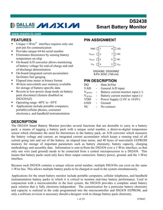
  • 1. DS2438 Smart Battery Monitor www.maxim-ic.com FEATURES PIN ASSIGNMENT ® § Unique 1-Wire interface requires only one port pin for communication GND 1 8 DQ § Provides unique 64-bit serial number VSENS+ NC § Eliminates thermistors by sensing battery 2 7 temperature on-chip VSENS- 3 6 NC § On-board A/D converter allows monitoring VAD 4 5 VDD of battery voltage for end-of-charge and end- of-discharge determination DS2438Z, DS2438AZ § On-board integrated current accumulator 8-Pin SOIC (150-mil) facilitates fuel gauging § Elapsed time meter in binary format PIN DESCRIPTION § 40-byte nonvolatile user memory available DQ - Data In/Out for storage of battery-specific data VAD - General A/D input § Reverts to low-power sleep mode on battery VSENS+ - Battery current monitor input (+) pack disconnect (feature disabled on VSENS- - Battery current monitor input (-) DS2438AZ) VDD - Power Supply (2.4V to 10.0V) § Operating range -40ºC to +85ºC GND - Ground § Applications include portable computers, NC - No connect portable/cellular phones, consumer electronics, and handheld instrumentation DESCRIPTION The DS2438 Smart Battery Monitor provides several functions that are desirable to carry in a battery pack: a means of tagging a battery pack with a unique serial number, a direct-to-digital temperature sensor which eliminates the need for thermistors in the battery pack, an A/D converter which measures the battery voltage and current, an integrated current accumulator which keeps a running total of all current going into and out of the battery, an elapsed time meter, and 40 bytes of nonvolatile EEPROM memory for storage of important parameters such as battery chemistry, battery capacity, charging methodology and assembly date. Information is sent to/from the DS2438 over a 1-Wire interface, so that only one wire (and ground) needs to be connected from a central microprocessor to a DS2438. This means that battery packs need only have three output connectors: battery power, ground, and the 1-Wire interface. Because each DS2438 contains a unique silicon serial number, multiple DS2438s can exist on the same 1-Wire bus. This allows multiple battery packs to be charged or used in the system simultaneously. Applications for the smart battery monitor include portable computers, cellular telephones, and handheld instrumentation battery packs in which it is critical to monitor real-time battery performance. Used in conjunction with a microcontroller in the host system, the DS2438 provides a complete smart battery pack solution that is fully chemistry-independent. The customization for a particular battery chemistry and capacity is realized in the code programmed into the microcontroller and DS2438 EEPROM, and only a software revision is necessary should a designer wish to change battery pack chemistry. 1 of 29 070605
  • 2. DS2438 ORDERING INFORMATION PART MARKING PACKAGE INFORMATION DS2438Z+ DS2438 8-Pin SOIC DS2438Z+T&R DS2438 DS2438Z+ on Tape-and-Reel DS2438AZ+ DS2438A 8-Pin SOIC DS2438AZ+T&R DS2438A DS2438AZ+ on Tape-and-Reel DS2438Z DS2438 8-Pin SOIC DS2438Z/T&R DS2438 DS2438Z on Tape-and-Reel DS2438AZ DS2438A 8-Pin SOIC DS2438AZ/T&R DS2438A DS2438AZ on Tape-and-Reel + Denotes lead-free package. DETAILED PIN DESCRIPTION PIN SYMBOL DESCRIPTION 1 GND Ground 2 VSENS+ Battery Input: connection for battery current to be monitored (see text) 3 VSENS- Battery Input: connection for battery current to be monitored (see text) 4 VAD ADC Input: input for general purpose A/D 5 VDD VDD Pin: input supply voltage 6, 7 NC No Connect 8 DQ Data Input/Out: for 1-Wire operation: Open drain OVERVIEW The block diagram of Figure 1 shows the seven major components of the DS2438: 1. 64-bit lasered ROM 2. temperature sensor 3. battery voltage A/D 4. battery current A/D 5. current accumulators 6. elapsed time meter 7. 40-byte nonvolatile user-memory Each DS2438 contains a unique 64-bit lasered ROM serial number so that several battery packs can be charged/monitored by the same host system. Furthermore, other Dallas products featuring the same 1-Wire bus architecture with a 64-bit ROM can reside on the same bus; refer to the Dallas Automatic Identification Data book for the specifications of these products. Communication to the DS2438 is via a 1-Wire port. With the 1-Wire port, the memory and control functions will not be available until the ROM function protocol has been established. The master must first provide one of four ROM function commands: 1) Read ROM, 2) Match ROM, 3) Search ROM, or 4) Skip ROM. These commands operate on the 64-bit lasered ROM portion of each device and can singulate a specific device if many are present on the 1-Wire line as well as to indicate to the bus master how many and what types of devices are present. After a ROM function sequence has been successfully executed, the memory and control functions are accessible and the master may then provide any one of the six memory and control function commands. 2 of 29
  • 3. DS2438 Control function commands may be issued which instruct the DS2438 to perform a temperature measurement or battery voltage A/D conversion. The result of these measurements will be placed in the DS2438’s memory map, and may be read by issuing a memory function command which reads the contents of the temperature and voltage registers. Additionally, the charging/discharging battery current is measured without user intervention, and again, the last completed result is stored in DS2438 memory space. The DS2438 uses these current measurements to update three current accumulators; the first stores net charge for fuel gauge calculations, the second accumulates the total charging current over the life of the battery, and the remaining accumulator tallies battery discharge current. The elapsed time meter data, which can be used in calculating battery self-discharge or time-related charge termination limits, also resides in the DS2438 memory map and can be extracted with a memory function command. The nonvolatile user memory of the DS2438 consists of 40 bytes of EEPROM. These locations may be used to store any data the user wishes and are written to using a memory function command. All data and commands are read and written least significant bit first. PARASITE POWER The block diagram (Figure 1) shows the parasite-powered circuitry. This circuitry “steals” power whenever the DQ pin is high. DQ will provide sufficient power as long as the specified timing and voltage requirements are met (see the section titled “1-Wire Bus System”). The advantage of parasite power is that the ROM may be read in absence of normal power, i.e., if the battery pack is completely discharged. DS2438 BLOCK DIAGRAM Figure 1 3 of 29
  • 4. DS2438 OPERATION-MEASURING TEMPERATURE The DS2438 measures temperatures through the use of an on-board temperature measurement technique. The temperature reading is provided in a 13-bit, two’s complement format, which provides 0.03125°C of resolution. Table 1 describes the exact relationship of output data to measured temperature. The data is transmitted serially over the 1-Wire interface. The DS2438 can measure temperature over the range of -55°C to +125°C in 0.03125°C increments. For Fahrenheit usage, a lookup table or conversion factor must be used. Note that temperature is represented in the DS2438 in terms of a 0.03125°C LSb, yielding the following 13-bit format. The 3 least significant bits of the Temperature Register will always be 0. The remaining 13 bits contain the two’s complement representation of the temperature in °C, with the MSb holding the sign (S) bit. See “Memory Map” section for the Temperature Register address location. Temperature Register Format Table 1 2-1 2-2 2-3 2-4 2-5 0 0 0 LSB MSb (unit = °C) LSb S 26 25 24 23 22 21 20 MSB TEMPERATURE DIGITAL OUTPUT (Binary) DIGITAL OUTPUT (Hex) +125°C 01111101 00000000 7D00h +25.0625°C 00011001 00010000 1910h +0.5°C 00000000 10000000 0080h 0°C 00000000 00000000 0000h -0.5°C 11111111 10000000 FF80h -25.0625°C 11100110 11110000 E6F0h -55°C 11001001 00000000 C900h OPERATION-MEASURING BATTERY VOLTAGE The on-board analog-to-digital converter (ADC) has 10 bits of resolution and will perform a conversion when the DS2438 receives a command protocol (Convert V) instructing it to do so. The result of this measurement is placed in the 2-byte Voltage Register. The range for the DS2438 ADC is 0 volt to 10 volt; this range is suitable for NiCd or NiMH battery packs up to six cells, and for lithium ion battery packs of two cells. The full-scale range of the ADC is scaled to 10.23 volt, resulting in a resolution of 10 mV. While the ADC has a range that extends down to 0 volt, it is important to note that the battery voltage can also be the supply voltage to the DS2438. As such, the accuracy of the ADC begins to degrade below battery voltages of 2.4 volt, and the ability to make conversions is limited by the operating voltage range of the DS2438. Voltage is expressed in this register in scaled binary format, as outlined in Table 2. Note that while codes exist for values below 2.4 volt, accuracy of the ADC and the limitation on the DS2438’s supply voltage make it unlikely that these values would be used in actual practice. See “Memory Map” section for the Voltage Register address location. 4 of 29
  • 5. DS2438 VOLTAGE REGISTER FORMAT Table 2 27 26 25 24 23 22 21 20 LSB MSb (unit = 10 mV) LSb 0 0 0 0 0 0 29 28 MSB BATTERY DIGITAL OUTPUT (Binary) DIGITAL OUTPUT (Hex) VOLTAGE 0.05V 0000 0000 0000 0101 0005h 2.7V 0000 0001 0000 1110 010Eh 3.6V 0000 0001 0110 1000 0168h 5V 0000 0001 1111 0100 01F4h 7.2V 0000 0010 1101 0000 02D0h 9.99V 0000 0011 1110 0111 03E7h 10V 0000 0011 1110 1000 03E8H For applications requiring a general purpose voltage A/D converter, the DS2438 can be configured so that the result of a Convert V command will place the scaled binary representation of the voltage on the VAD input (as opposed to the VDD input) into the Voltage Register in the same format described in Table 2. Depending upon the state of the Status/Configuration Register, either (but not both) the VDD or VAD voltage will be stored in the Voltage Register upon receipt of the Convert V command. Refer to the description of the Status/Configuration Register in the Memory Map section for details. If the VAD input is used as the voltage input, the A/D will be accurate for 1.5V < VAD < 2VDD over the range 2.4V < VDD < 5.0V. This feature gives the user the ability to have a voltage A/D that meets spec accuracy for inputs over the entire range of 1.5V < VAD < 10V for VDD = 5.0V. OPERATION - MEASURING BATTERY CURRENT The DS2438 features an A/D converter that effectively measures the current flow into and out of the battery pack by measuring the voltage across an external sense resistor. It does so in the background at a rate of 36.41 measurements/sec; thus, no command is required to initiate current flow measurements. However, the DS2438 will only perform current A/D measurements if the IAD bit is set to “1” in the Status/Configuration Register. The DS2438 measures current flow in and out of the battery through the VSENS pins; the voltage from the VSENS+ pin to the VSENS- pin is considered to be the voltage across the current sense resistor, RSENS. The VSENS+ terminal may be tied directly to the RSENS resistor, however, for VSENS-, we recommend use of an RC low pass filter between it and the GND end of RSENS (see the block diagram in Figure 1). Using a 100 kW (min) resistor (RF) and a 0.1 mF tantalum capacitor (CF), the filter cutoff is approximately 15.9 Hz. The current A/D measures at a rate of 36.41 times per second, or once every 27.46 ms. This filter will capture the effect of most current spikes, and will thus allow the current accumulators to accurately reflect the total charge which has gone into or out of the battery. The voltage across current sense resistor RSENS is measured by the ADC and the result is placed in the Current Register in two’s complement format. The sign (S) of the result, indicating charge or discharge, resides in the most significant bit of the Current Register, as shown in Table 3. See “Memory Map” in Figure 7 for the Current Register address location. 5 of 29
  • 6. DS2438 CURRENT REGISTER FORMAT Table 3 (This register actually stores the voltage measured across current sense resistor RSENS. This value can be used to calculate battery pack current using the equation below.) 27 26 25 24 23 22 21 20 LSB MSb (unit = 0.2441mV) LSb S S S S S S 29 28 MSB The battery pack current is calculated from the Current Register value using the equation: I = Current Register / (4096 * RSENS) (where RSENS is in W) For example, if 1.25A is flowing into the pack, and the pack uses a 0.025W sense resistor, the DS2438 will write the value 12810 to the Current Register. From this value, battery pack current can be calculated to be: I = 128 / ( 4096 * 0.025) = 1.25A Because small current ADC offset errors can have a large cumulative effect when current is integrated over time, the DS2438 provides a method for canceling offset errors in the current ADC. After each current measurement is completed, the measured value is added to the contents of the Offset Register and the result is then stored in the Current Register. The Offset Register is a two-byte nonvolatile read/write register formatted in two’s-complement format. The four MSb’s of the register contain the sign of the offset, as shown in Table 4. OFFSET REGISTER FORMAT Table 4 24 23 22 21 20 0 0 0 LSB MSb (unit = 0.2441 mV) LSb X X X S 28 27 26 25 MSB The following process can be used to calibrate the current ADC: 1. Write all zeroes to the Offset Register 2. Force zero current through RSENS 3. Read the Current Register value 4. Disable the current ADC by setting the IAD bit in the Status/Configuration Register to “0” 5. Change the sign of the previously-read Current Register value by performing the two’s complement and write the result to the Offset Register 6. Enable the current ADC by setting the IAD bit in the Status/Configuration Register to “1” NOTE: When writing to the Offset Register, current measurement MUST be disabled (IAD bit set to “0”). The current ADC calibration process is done for each DS2438 device prior to shipment. However, for best results, battery pack manufacturers should calibrate the current ADC during initial battery pack testing, and the host system should calibrate whenever possible (during battery charging, for example). 6 of 29
  • 7. DS2438 OPERATION - CURRENT ACCUMULATORS The DS2438 tracks the remaining capacity of a battery using the Integrated Current Accumulator (ICA). The ICA maintains a net accumulated total of current flowing into and out of the battery; therefore, the value stored in this register is an indication of the remaining capacity in a battery and may be used in performing fuel gauge functions. In addition, the DS2438 has another register that accumulates only charging (positive) current (CCA) and one that accumulates only discharging (negative) current (DCA). The CCA and DCA give the host system the information needed to determine the end of life of a rechargeable battery, based on total charge/discharge current over its lifetime. The current measurement described above yields the voltage across sense resistor RSENS measured every 27.46 ms. This value is then used to increment or decrement the ICA register, increment the CCA (if current is positive), or increment the DCA (if current is negative). The ICA is a scaled 8-bit volatile binary counter that integrates the voltage across RSENS over time. The ICA is only incremented/decremented if the IAD bit is set to 1 in the Status/Configuration Register. Table 5 illustrates the contents of the ICA. See Memory Map section for the address location of the ICA. ICA REGISTER FORMAT Table 5 (This register accumulates the voltage measured across current sense resistor RSENS. This value can be used to calculate remaining battery capacity using the equation below.) 27 26 25 24 23 22 21 20 MSb (unit = 0.4882 mVhr) LSb Remaining battery capacity is calculated from the ICA value using the equation: Remaining Capacity = ICA / (2048 * RSENS) (where RSENS is in W) For example, if a battery pack has 0.625 Ahr of remaining capacity, and the pack uses a 0.025W sense resistor, the ICA will contain the value 32. From this value, remaining capacity can be calculated to be: Remaining Capacity = 32 / ( 2048 * 0.025) = 0.625 Ahr Since the accuracy of the current ADC is +2 LSb, measurements of very small currents can be inaccurate by a high percentage. Because these inaccuracies can turn into large ICA errors when accumulated over a long period of time, the DS2438 provides a method for filtering out potentially erroneous small signals so that they are not accumulated. The DS2438’s Threshold Register specifies a current measurement magnitude (after offset cancellation) above which the measurement is accumulated in the ICA, CCA and DCA and below which it is not accumulated. The format of the Threshold Register is shown in Table 6. The power-on default Threshold Register value is 00h (no threshold). NOTE: When writing to the Threshold Register, current measurement must be disabled (IAD bit set to “0”). 7 of 29
  • 8. DS2438 THRESHOLD REGISTER FORMAT Table 6 TH2 TH1 0 0 0 0 0 0 MSb LSb TH2 TH1 THRESHOLD 0 0 None (default) 0 1 ±2 LSB 1 0 ±4 LSB 1 1 ±8 LSB The Charging Current Accumulator (CCA) is a two-byte nonvolatile read/write counter which represents the total charging current the battery has encountered in its lifetime. It is only updated when current through RSENS, is positive; i.e., when the battery is being charged. Similarly, the Discharge Current Accumulator (DCA) is a two-byte nonvolatile counter which represents the total discharging current the battery has encountered over its lifetime. The CCA and DCA can be configured to function in any of three modes: disabled, enabled with shadow- to-EEPROM, and enabled without shadow-to-EEPROM. When the CCA and DCA are disabled (by setting either the IAD bit or the CA bit in the Status/Configuration Register to “0”), the memory in page 07h is free for general purpose data storage. When the CCA and DCA are enabled (by setting both IAD and CA to “1”), page 07h is reserved for these registers, and none of the bytes in page 07h should be written to via the 1-Wire bus. When the CCA and DCA are enabled, their values are automatically shadowed to EEPROM memory by setting the EE bit in the Status/Configuration Register to “1”. When these registers are configured to shadow to EEPROM, the information will accumulate over the lifetime of the battery pack and will not be lost when the battery becomes discharged. Shadow-to-EEPROM is disabled when the EE bit is “0”. Table 7 illustrates the format of the CCA and DCA registers. Table 8 summarizes the modes of operation for ICA, CCA and DCA. CCA/DCA REGISTER FORMAT Table 7 27 26 25 24 23 22 21 20 LSB MSb (unit = 15.625 mVHr) LSb 215 214 213 212 211 210 29 28 MSB ICA/CCA/DCA MODES OF OPERATION Table 8 IAD Bit CA Bit EE Bit ICA CCA/DCA CCA/DCA Copy- to-EEPROM 0 X X Inactive Inactive Inactive 1 0 X Active Inactive Inactive 1 1 0 Active Active Inactive 1 1 1 Active Active Active 8 of 29
  • 9. DS2438 Figure 2 illustrates the activity of the ICA, CCA, and DCA over a sample charge/discharge cycle of a battery pack, assuming the DS2438 is configured for the ICA to function and the CCA/DCA to function and shadow data to EEPROM. To simplify the illustration of the accumulators, they are treated as analog values, although they are digital counters in the DS2438. Note that when the battery becomes fully discharged, i.e., the ICA value reaches 0, the CCA and DCA register values are maintained. CURRENT ACCUMULATOR ACTIVITY Figure 2 SENSE RESISTOR SELECTION The selection of RSENS involves a tradeoff. On the one hand, the impedance of RSENS must be minimized to avoid excessive voltage drop during peak current demands. On the other hand, the impedance of RSENS should be maximized to achieve the finest resolution for current measurement and accumulation. Table 9 below lists several example RSENS values, the LSb of the current calculation ( 1/(4096 * RSENS) ) and the LSb of the remaining capacity calculation ( 1/(2048 * RSENS) ). The user should carefully consider voltage drop at maximum current and required current measurement/accumulation resolution when selecting RSENS. SENSE RESISTOR TRADEOFFS Table 9 SENSE RESISTOR REMAINING MAX REMAINING VALUE (RSENS) CURRENT lsb CAPACITY lsb CAPACITY VALUE 25 mW 9.76 mA 19.53 mAHr 5000 mAhr 50 mW 4.88 mA 9.76 mAHr 2500 mAhr 100 mW 2.44 mA 4.88 mAHr 1250 mAhr 200 mW 1.22 mA 2.44 mAHr 625 mAhr OPERATION - ELAPSED TIME METER An internal oscillator is used as the timebase for the timekeeping functions. The elapsed time functions are double buffered, allowing the master to read elapsed time without the data changing while it is being read. To accomplish this, a snapshot of the counter data is transferred to holding registers which the user accesses. This occurs after the 8th bit of the Recall Memory command. The elapsed time meter (ETM) is a 4-byte binary counter with 1-second resolution. The ETM can accumulate 136 years of seconds before rolling over. Time/date is represented by the number of seconds since a reference point, which is determined by the user. For example, 12:00 A.M., January 1, 1970 could be used as a reference point. 9 of 29
  • 10. DS2438 Two other time-related functions are available. The first is the Disconnect Timestamp, which is written to by the DS2438 whenever it senses that the DQ line has been low for approximately 2 seconds. This condition would signal that the battery pack has been removed from the system; the time when that occurs is written into the Disconnect Timestamp register, so that upon replacement into the system, the system can determine how long the device has been in storage, to facilitate self-discharge corrections to the remaining battery capacity. After the disconnect has been detected, the DS2438 reverts to a sleep mode, during which nothing is active except the real time clock. Some applications may prefer that the data converters and current accumulators continue operation following a pack disconnect. Thus, a version of the DS2438 (part number DS2438A) is offered for those applications. Other than not reverting to a low-power sleep mode following disconnect, there are no specification differences between the DS2438 and the DS2438A. The other timestamp is the End-of-Charge timestamp, which is written to by the DS2438 whenever it senses that charging is finished (when current changes direction). This timestamp allows the user to calculate the amount of time the battery has been in a discharge or storage state, again to facilitate self- discharge calculations. The format of the ETM, Disconnect, and End-of-Charge registers are as shown in Table 10. Refer to the “Memory Map” section for the address location of the time-related registers. TIME REGISTER FORMAT Table 10 27 26 25 24 23 22 21 20 LSB MSb (unit = 1s) LSb 215 214 213 212 211 210 29 28 MSb (unit = 1s) LSb 223 222 221 220 219 218 217 216 MSb (unit = 1s) LSb 231 230 229 228 227 226 225 224 MSB 64-BIT LASERED ROM Each DS2438 contains a unique ROM code that is 64 bits long. The first 8 bits are a 1-Wire family code (DS2438 code is 26h). The next 48 bits are a unique serial number. The last 8 bits are a CRC of the first 56 bits. (See Figure 3.) The 64-bit ROM and ROM Function Control section allow the DS2438 to operate as a 1-Wire device and follow the 1-Wire protocol detailed in the section “1-Wire Bus System.” The functions required to control sections of the DS2438 are not accessible until the ROM function protocol has been satisfied. This protocol is described in the ROM function protocol flow chart (Figure 5). The 1-Wire bus master must first provide one of four ROM function commands: 1) Read ROM, 2) Match ROM, 3) Search ROM, or 4) Skip ROM. After a ROM function sequence has been successfully executed, the functions specific to the DS2438 are accessible and the bus master may then provide any one of the six memory and control function commands. 10 of 29
  • 11. DS2438 64-BIT LASERED ROM FORMAT Figure 3 8-BIT CRC CODE 48-BIT SERIAL NUMBER 8-BIT FAMILY CODE (26h) MSb LSb MSb LSb MSb LSb CRC Generation The DS2438 has an 8-bit CRC stored in the most significant byte of the 64-bit ROM. The bus master can compute a CRC value from the first 56 bits of the 64-bit ROM and compare it to the value stored within the DS2438 to determine if the ROM data has been received error-free by the bus master. The equivalent polynomial function of this CRC is: CRC = X8 + X5 + X4 +1 The DS2438 also generates an 8-bit CRC value using the same polynomial function shown above and provides this value to the bus master to validate the transfer of data bytes. In each case where a CRC is used for data transfer validation, the bus master must calculate a CRC value using the polynomial function given above and compare the calculated value to either the 8-bit CRC value stored in the 64-bit ROM portion of the DS2438 (for ROM reads) or the 8-bit CRC value computed within the DS2438 (which is read as a 9th byte when a scratchpad is read). The comparison of CRC values and decision to continue with an operation are determined entirely by the bus master. There is no circuitry inside the DS2438 that prevents a command sequence from proceeding if the CRC stored in or calculated by the DS2438 does not match the value generated by the bus master. Proper use of the CRC as outlined in the flowchart of Figure 6 can result in a communication channel with a very high level of integrity. The 1-Wire CRC can be generated using a polynomial generator consisting of a shift register and XOR gates as shown in Figure 4. Additional information about the Dallas 1-Wire Cyclic Redundancy Check is available in Application Note 27 entitled “Understanding and Using Cyclic Redundancy Checks with Dallas Semiconductor Touch Memory Products.” The shift register bits are initialized to 0. Then starting with the least significant bit of the family code, 1 bit at a time is shifted in. After the 8th bit of the family code has been entered, the serial number is entered. After the 48th bit of the serial number has been entered, the shift register contains the CRC value. 1-WIRE CRC CODE Figure 4 11 of 29
  • 12. DS2438 ROM FUNCTIONS FLOWCHART Figure 5 12 of 29
  • 13. DS2438 MEMORY/CONTROL FUNCTIONS FLOWCHART Figure 6 NO YES 13 of 29
  • 14. DS2438 MEMORY/CONTROL FUNCTIONS FLOWCHART Figure 6 (continued) MEMORY MAP The DS2438’s memory is organized as shown in Figure 7. The memory consists of a scratchpad RAM and storage SRAM/EEPROM. The scratchpad helps insure data integrity when communicating over the 1-Wire bus. Data is first written to the scratchpad where it can be read back. After the data has been verified, a copy scratchpad command will transfer the data to the appropriate page in memory (pages 0-2 are primarily volatile SRAM, pages 3-7 are EEPROM). This process insures data integrity when modifying the memory. The DS2438’s memory is organized as 64 bytes of memory, in eight 8-byte pages. Each page has its own scratchpad space, organized as 8 bytes of memory. When reading a scratchpad, there is a 9th byte which may be read with a Read Scratchpad command. This byte contains a cyclic redundancy check (CRC) byte, which is the CRC over all of the 8 bytes in the currently selected scratchpad. This CRC is implemented in the fashion described in the section titled “CRC Generation.” 14 of 29
  • 15. DS2438 Page 0 (00h) The first page contains the most frequently accessed information of the DS2438, and most locations are volatile read-only bytes with the exception of the Status/Configuration Register (Byte 0) and the Threshold Register (Byte 7). The Status/Configuration Register is a nonvolatile read/write byte which defines which features of the DS2438 are enabled and how they will function. The register is formatted as follows: X ADB NVB TB AD EE CA IAD MSb LSb IAD = Current A/D Control Bit. “1” = the current A/D and the ICA are enabled, and current measurements will be taken at the rate of 36.41 Hz; “0” = the current A/D and the ICA have been disabled. The default value of this bit is a “1” (current A/D and ICA are enabled). CA = Current Accumulator Configuration. “1” = CCA/DCA is enabled, and data will be stored and can be retrieved from page 7, bytes 4-7; “0” = CCA/DCA is disabled, and page 7 can be used for general EEPROM storage. The default value of this bit is a “1” (current CCA/DCA are enabled). EE = Current Accumulator Shadow Selector bit. “1” = CCA/DCA counter data will be shadowed to EEPROM each time the respective register is incremented; “0”= CCA/DCA counter data will not be shadowed to EEPROM. The CCA/DCA could be lost as the battery pack becomes discharged. If the CA bit in the status/configuration register is set to “0”, the EE bit will have no effect on the DS2438 functionality. The default value of this bit is a “1” (current CCA/DCA data shadowed to EEPROM). AD = Voltage A/D Input Select Bit. “1” = the battery input (VDD) is selected as the input for the DS2438 voltage A/D converter; “0” = the general purpose A/D input (VAD) is selected as the voltage A/D input. For either setting, a Convert V command will initialize a voltage A/D conversion. The default value of this bit is a “1” (VDD is the input to the A/D converter). TB = Temperature Busy Flag. “1” = temperature conversion in progress; “0” = temperature conversion complete. NVB = Nonvolatile Memory Busy Flag. “1” = Copy from Scratchpad to EEPROM in progress; “0” = Nonvolatile memory not busy. A copy to EEPROM may take from 2 ms to 10 ms (taking longer at lower supply voltages). ADB = A/D Converter Busy Flag. “1” = A/D conversion in progress on battery voltage; “0” = conversion complete, or no measurement being made. An A/D conversion takes approximately 10 ms. X = Don’t care Bytes 1 and 2 of page 0 contain the last completed temperature conversion in the format described in the “Operation - Measuring Temperature” section. Bytes 3-4 contain the last completed voltage A/D conversion result and bytes 5-6 contain the instantaneous current data. Byte 7 contains the Threshold Register. Refer to the appropriate section for the data format of these locations. NOTE: The data in the scratchpad of the status and threshold register will determine the operation of the device. 15 of 29
  • 16. DS2438 Page 1 (01h) The second page, Page 1, contains the ICA, elasped time meter, and current offset data. Both the ETM and ICA are volatile read/write locations so that they may be set, changed, or cleared by the host software. Bytes 0-3 contain the ETM data, formatted as described in the “Operation - Elapsed Time Meter” section. Byte 4 contains the 8-bit ICA. Bytes 5 and 6 contain the Offset Register data. Byte 7 is reserved and will read out as all “1”s. Page 2 (02h) The third page of memory (Page 2) contains the Disconnect (first 4 bytes) and End of Charge (remaining 4 bytes) timestamps. This page is volatile and read/write. Refer to the “Operation – Elapsed Time Meter” section for the formatting of these locations. Pages 3-7 (03h - 07h) The remainder of the memory in the DS2438 (Pages 3 through 7) is backed with EEPROM. This memory provides 40 bytes of user memory which may be used to carry any information the user wishes to store. Additionally, the CCA/DCA information is stored in bytes 4-7 of page 7 if the DS2438 is configured appropriately. If the CCA/DCA is used, page 7 should not be written to or current accumulator data will be overwritten. See “Operation-Current Accumulators” for details. MEMORY MAP Figure 7 PAGE BYTE CONTENTS R/W NV PAGE BYTE CONTENTS R/W NV 0 STATUS/ R/W YES 0 USER BYTE R/W YES CONFIGURATION 1 TEMPERATURE R NO 1 USER BYTE R/W YES LSB 2 TEMPERATURE R NO 2 USER BYTE R/W YES MSB 0 3 VOLTAGE LSB R NO 3 3 USER BYTE R/W YES 4 VOLTAGE MSB R NO 4 USER BYTE R/W YES 5 CURRENT LSB R NO 5 USER BYTE R/W YES 6 CURRENT MSB R NO 6 USER BYTE R/W YES 7 THRESHOLD R/W YES 7 USER BYTE R/W YES 0 ETM BYTE 0 R/W NO 0 USER BYTE R/W YES 1 ETM BYTE 1 R/W NO 1 USER BYTE R/W YES 2 ETM BYTE 2 R/W NO 2 USER BYTE R/W YES 1 3 ETM BYTE 3 R/W NO 3 USER BYTE R/W YES 4 ICA R/W NO 4 4 USER BYTE R/W YES 5 OFFSET LSB R/W YES 5 USER BYTE R/W YES 6 OFFSET MSB R/W YES 6 USER BYTE R/W YES 7 RESERVED 7 USER BYTE R/W YES R/W NO 0 DISCONNECT R/W NO · · · · · BYTE 0 1 DISCONNECT R/W NO · · · · · BYTE 1 2 DISCONNECT R/W NO · · · · · BYTE 2 2 3 DISCONNECT R/W NO 0 USER BYTE R/W YES BYTE 3 4 END OF CHARGE R/W NO 1 USER BYTE R/W YES BYTE 0 5 END OF CHARGE R/W NO 2 USER BYTE R/W YES BYTE 1 6 END OF CHARGE R/W NO 7 3 USER BYTE R/W YES BYTE 2 7 END OF CHARGE R/W NO 4 USER BYTE/ R/W YES BYTE 3 CCA LSB 5 USER BYTE/ R/W YES CCA MSB 6 USER BYTE/ R/W YES DCA LSB 7 USER BYTE/ R/W YES DCA MSB 16 of 29
  • 17. DS2438 1-Wire BUS SYSTEM The 1-Wire bus is a system which has a single bus master and one or more slaves. The DS2438 behaves as a slave. The discussion of this bus system is broken down into three topics: hardware configuration, transaction sequence, and 1-Wire signaling (signal types and timing). HARDWARE CONFIGURATION The 1-Wire bus has only a single line by definition; it is important that each device on the bus be able to drive it at the appropriate time. To facilitate this, each device attached to the 1-Wire bus must have open drain or 3-state outputs. The 1-Wire port of the DS2438 (DQ pin) is open drain with an internal circuit equivalent to that shown in Figure 8. A multidrop bus consists of a 1-Wire bus with multiple slaves attached. The 1-Wire bus requires a pull-up resistor of approximately 5 kW. HARDWARE CONFIGURATION Figure 8 The idle state for the 1 wire bus is high. If for any reason a transaction needs to be suspended, the bus MUST be left in the idle state if the transaction is to resume. Infinite recovery time can occur between bits so long as the 1-Wire bus is in the inactive (high) state during the recovery period. If this does not occur and the bus is left low, all components on the bus will be reset. See Wire-1 Reset Pulse Timing (Figure 9). TRANSACTION SEQUENCE The protocol for accessing the DS2438 via the 1-Wire port is as follows: § Initialization § ROM Function Command § Memory Function Command § Transaction/Data INITIALIZATION All transactions on the 1-Wire bus begin with an initialization sequence. The initialization sequence consists of a reset pulse transmitted by the bus master followed by presence pulse(s) transmitted by the slave(s). The presence pulse lets the bus master know that the DS2438 is on the bus and is ready to operate. For more details, see the “1-Wire Signaling” section. 17 of 29
  • 18. DS2438 ROM FUNCTION COMMANDS Once the bus master has detected a presence, it can issue one of the four ROM function commands. All ROM function commands are 8-bits long. A list of these commands follows (refer to flowchart in Figure 5): Read ROM [33h] This command allows the bus master to read the DS2438’s 8-bit family code (26h), unique 48-bit serial number, and 8-bit CRC. This command can only be used if there is a single DS2438 on the bus. If more than one slave is present on the bus, a data collision will occur when all slaves try to transmit at the same time (open-drain will produce a wired-AND result). Match ROM [55h] The Match ROM command, followed by a 64-bit ROM sequence, allows the bus master to address a specific DS2438 on a multidrop bus. Only the DS2438 that exactly matches the 64-bit ROM sequence will respond to the following memory function command. All slaves that do not match the 64-bit ROM sequence will wait for a reset pulse. This command can be used with a single or multiple devices on the bus. Skip ROM [CCh] This command can save time in a single-drop bus system by allowing the bus master to access the memory functions without providing the 64-bit ROM code. If more than one slave is present on the bus and a read command is issued following the Skip ROM command, data collision will occur on the bus as multiple slaves transmit simultaneously (open drain pull-downs will produce a wired-AND result). Search ROM [F0h] When a system is initially brought up, the bus master might not know the number of devices on the 1- Wire bus or their 64-bit ROM codes. The search ROM command allows the bus master to use a process of elimination to identify the 64-bit ROM codes of all slave devices on the bus. Example of a ROM Search The ROM search process is the repetition of a simple three-step routine: read a bit, read the complement of the bit, then write the desired value of that bit. The bus master performs this simple, three-step routine on each bit of the ROM. After one complete pass, the bus master knows the contents of the ROM in one device. The remaining number of devices and their ROM codes may be identified by additional passes. The following example of the ROM search process assumes four different devices are connected to the same 1-Wire bus. The ROM data of the four devices is as shown (LSb first): ROM1 = 00110101... ROM2 = 10101010... ROM3 = 11110101... ROM4 = 00010001... The search process is as follows: 1. The bus master begins the initialization sequence by issuing a reset pulse. The slave devices respond by issuing simultaneous presence pulses. 2. The bus master will then issue the search ROM command on the 1-Wire bus (F0h). 18 of 29
  • 19. DS2438 3. The bus master reads a bit from the 1-Wire bus. Each device will respond by placing the value of the first bit of their respective ROM data onto the 1-Wire bus. ROM1 and ROM4 will place a 0 onto the 1-Wire bus, i.e., pull it low. ROM2 and ROM3 will place a 1 onto the 1-Wire bus by allowing the line to stay high. The result is the logical AND of all devices on the line; therefore the bus master sees a 0. The bus master reads another bit. Since the Search ROM data command is being executed, all of the devices on the 1-Wire bus respond to this second read by placing the complement of the first bit of their respective ROM data onto the 1-Wire bus. ROM1 and ROM4 will place a 1 onto the 1-wire, allowing the line to stay high. ROM2 and ROM3 will place a 0 onto the 1-wire, thus it will be pulled low. The bus master again observes a 0 for the complement of the first ROM data bit. The bus master has determined that there are some devices on the 1-Wire bus that have a 0 in the first position and others that have a 1. The data obtained from the two reads of the three-step routine have the following interpretations: 00 - There are still devices attached which have conflicting bits in this position. 01 - All devices still coupled have a 0 bit in this bit position. 10 - All devices still coupled have a 1 bit in this bit position. 11 - There are no devices attached to the 1-Wire bus. 4. The bus master writes a 0. This deselects ROM2 and ROM3 for the remainder of this search pass, leaving only ROM1 and ROM4 connected to the 1-Wire bus. 5. The bus master performs two more reads and receives a 0 bit followed by a 1 bit. This indicates that all devices still coupled to the bus have 0s as their second ROM data bit. 6. The bus master then writes a 0 to keep both ROM1 and ROM4 coupled. 7. The bus master executes two reads and receives two 0 bits. This indicates that both 1 bits and 0 bits exist as the 3rd bit of the ROM data of the attached devices. 8. The bus master writes a 0 bit. This deselects ROM1, leaving ROM4 as the only device still connected. 9. The bus master reads the remainder of the ROM bits for ROM4 and continues to access the part if desired. This completes the first pass and uniquely identifies one part on the 1-Wire bus. 10. The bus master starts a new ROM search sequence by repeating steps 1 through 7. 11. The bus master writes a 1 bit. This decouples ROM4, leaving only ROM1 still coupled. 12. The bus master reads the remainder of the ROM bits for ROM1 and communicates to the underlying logic if desired. This completes the second ROM search pass, in which another of the ROMs was found. 13. The bus master starts a new ROM search by repeating steps 1 through 3. 14. The bus master writes a 1 bit. This deselects ROM1 and ROM4 for the remainder of this search pass, leaving only ROM2 and ROM3 coupled to the system. 15. The bus master executes two read time slots and receives two 0s. 19 of 29
  • 20. DS2438 16. The bus master writes a 0 bit. This decouples ROM3, and leaving only ROM2. 17. The bus master reads the remainder of the ROM bits for ROM2 and communicates to the underlying logic if desired. This completes the third ROM search pass, in which another of the ROMs was found. 18. The bus master starts a new ROM search by repeating steps 13 through 15. 19. The bus master writes a 1 bit. This decouples ROM2, leaving only ROM3. 20. The bus master reads the remainder of the ROM bits for ROM3 and communicates to the underlying logic if desired. This completes the fourth ROM search pass, in which another of the ROMs was found. Note that the bus master learns the unique ID number (ROM data pattern) of one 1-Wire device on each ROM Search operation. The time required to derive the part’s unique ROM code is: 960 ms + (8 + 3 x 64) 61 ms = 13.16 ms The bus master is therefore capable of identifying 75 different 1-Wire devices per second. MEMORY COMMAND FUNCTIONS The following command protocols are summarized in Table 11, and by the flowchart of Figure 6. Write Scratchpad [4Ehxxh] This command writes to the scratchpad page xxh of the DS2438. The entire 8-byte scratchpad space may be written, but all writing begins with the byte present at address 0 of the selected scratchpad. After issuing this command, the user must send the page number of the scratchpad to be written; then the user may begin writing data to the DS2438 scratchpad. Writing may be terminated at any point by issuing a reset. Valid page numbers for writing are 00h-07h. Read Scratchpad [BEhxxh] This command reads the contents of the scratchpad page xxh on the DS2438. After issuing this command, the user must send the page number of the scratchpad to be read, and then may begin reading the data, always beginning at address 0 of the selected scratchpad. The user may read through the end of the scratchpad space (byte 07h), with any reserved data bits reading all logic 1s, then read the CRC of the data, and after which the data read will be all logic 1s. If not all locations are to be read, the master may issue a reset to terminate reading at any time. Valid page numbers are 00h - 07h. Copy Scratchpad [48hxxh] This command copies the scratchpad page xxh into the EEPROM / SRAM memory page xxh of the DS2438. After issuing this command, the user must write a page number to direct which page of memory the scratchpad is to be copied. Valid page numbers are 00h - 07h. During the copy function, the NVB bit in the Status/Configuration register will be set to a “l”. When the copy is complete, this bit will reset to “0”. If the bus master issues read time slots following this command, the DS2438 will output “0” on the bus as long as it is busy copying the scratchpad to SRAM/EEPROM; it will return a “1” when the copy process is complete. 20 of 29
  • 21. DS2438 Recall Memory [B8hxxh] This command recalls the stored values in EEPROM / SRAM page xxh to the scratchpad page xxh. This command must proceed a Read SPxx command in order to read any page of memory on the DS2438. Valid page numbers are 00h - 07h. Convert T [44h] This command begins a temperature conversion. No further data is required. The temperature conversion will be performed, setting the TB flag in the Status/Configuration register to a “1” during conversion. When the temperature conversion is done, the TB flag will clear to a “0”. If the bus master issues read time slots following this command, the DS2438 will output “0” on the bus as long as it is busy making a temperature conversion; it will return a “1” when the temperature conversion is complete. Convert V [B4h] This command instructs the DS2438 to initiate a voltage analog-to-digital conversion cycle. This sets the ADB flag (see Status/Configuration register discussion in the Memory Map section). The voltage supply that is measured is defined by the AD bit of the Status/Configuration register. When the A/D conversion is done, the ADB flag is cleared and the current voltage value is placed in the VOLTAGE REGISTER of page 00h. While an A/D conversion is taking place, all other memory functions are still available for use. If the bus master issues read time slots following this command, the DS2438 will output “0” on the bus as long as it is busy making a voltage measurement; it will return a “1” when the conversion is complete. DS2438 COMMAND SET Table 11 INSTRUCTION DESCRIPTION PROTOCOL 1-WIRE BUS 1-WIRE BUS MASTER STATUS DATA AFTER AFTER ISSUING ISSUING PROTOCOL PROTOCOL MEMORY COMMANDS Read Scratchpad Reads bytes from BEh <page Rx <read up to nine DS2438 Scratchpad 00h-07h> bytes of data> page xxh Write Scratchpad Writes bytes to 4Eh <page Tx <write up to eight DS2438 00h-07h> bytes of data> Scratchpad page xxh Copy Scratchpad Copies entire contents 48h<page Idle or Rx of NVB bit {NVB bit in Status of Scratchpad page 00h-07h> Register = 1 until xxh copy complete (2- to 8-byte EEPROM/ 10 ms, typ)} SRAM page xxh Recall Memory Copies entire contents B8h<page Idle Idle of EEPROM/SRAM 00h-07h> page xxh to Scratchpad page xxh REGISTER COMMANDS Convert T Initiates temperature 44h Idle or Rx of TB bit {TB bit in Status conversion Register = 1 until conversion complete} Convert V Initiates voltage A/D B4h Idle or Rx of ADB bit {ADB bit in Status conversion Register = 1 until conversion complete} 21 of 29
  • 22. DS2438 NOTES: 1. Temperature conversion takes up to 10 ms. 2. A/D conversion takes up to 4 ms. 3. EEPROM writes take up to 10 ms. SAMPLE COMMAND SEQUENCE Table 12 Example: Bus Master enables the ICA, CCA, and DCA on a single DS2438 and configures it such that the CCA/DCA information is shadowed to EEPROM. The voltage A/D is configured such that the DS2438 will perform voltage measurements on the battery (VDD) voltage. MASTER MODE DATA (LSB FIRST) COMMENTS TX Reset Read pulse RX Presence Presence pulse TX CCh Skip ROM TX 4Eh00h Issue Write SP 00h command TX 0Fh Sets ICA, CA, EE, AD Bits active TX Reset Reset pulse RX Presence Presence pulse TX CCh Skip ROM TX BEh00h Issue Read SP 00h command RX <9 data bytes> Read scratchpad data and CRC TX Reset Reset pulse RX Presence Presence pulse TX CCh Skip ROM TX 48h00h Issue Copy SP 00h command RX Read Slots DS2438 returns a “1” when Copy SP is complete TX Reset Reset pulse RX Presence Presence Pulse, done 22 of 29
  • 23. DS2438 SAMPLE COMMAND SEQUENCE Table 13 Example: Bus Master issues a temperature and voltage conversion, then reads the temperature, battery voltage, battery current, all on a single DS2438. MASTER MODE DATA (LSB FIRST) COMMENTS TX Reset Reset pulse RX Presence Presence pulse TX CCh Skip ROM TX 44h Issue Convert Temperature command, Read Slots TX Reset Reset pulse RX Presence Presence pulse TX CCh Skip ROM TX B4h Issue Convert Voltage command, Read Slots TX Reset Reset pulse RX Presence Presence pulse TX CCh Skip ROM TX B8h00h Issue Recall Memory page 00h command TX Reset Reset pulse RX Presence Presence pulse TX CCh Skip ROM TX BEh00h Issue Read SP 00h command RX <9 data bytes> Read scratchpad data and CRC. This page contains temperature, voltage, and current measurements. TX Reset Reset pulse RX Presence Presence pulse, done 23 of 29
  • 24. DS2438 SAMPLE COMMAND SEQUENCE Table 14 Example: Assuming a single DS2438 is configured for its current accumulators to function, this sequence allows the Bus Master to read the three current accumulators. MASTER MODE DATA (LSB FIRST) COMMENTS TX Reset Reset pulse RX Presence Presence pulse TX CCh Skip ROM TX B8h01h Issue Recall Memory page 01h command TX Reset Reset pulse RX Presence Presence pulse TX CCh Skip ROM TX BEh01h Issue Read SP 01h command RX <9 data bytes> Read scratchpad data and CRC. The ICA is located in byte 04h TX Reset Reset pulse RX Presence Presence pulse TX CCh Skip ROM TX B8h07h Issue Recall Memory page 07h command TX Reset Reset pulse RX Presence Presence pulse TX CCh Skip ROM TX B8h07h Issue Read SP 07h command RX <9 data bytes> Read scratchpad data and CRC. The CCA is located in bytes 04h-05h and the DCA is located in bytes 06h-07h. TX Reset Reset pulse RX Presence Presence pulse, done I/O SIGNALING The DS2438 requires strict protocols to insure data integrity. The protocol consists of several types of signaling on one line: reset pulse, presence pulse, write 0, write 1, read 0, and read 1. All of these signals, with the exception of the presence pulse, are initiated by the bus master. The initialization sequence required to begin any communication with the DS2438 is shown in Figure 9. A reset pulse followed by a presence pulse indicates the DS2438 is ready to send or receive data given the correct ROM command and memory function command. The bus master transmits (Tx) a reset pulse (a low signal for a minimum of 480 ms). The bus master then releases the line and goes into a receive mode(Rx). The 1-Wire bus is pulled to a high state via the 5 kW pull-up resistor. After detecting the rising edge on the I/O pin, the DS2438 waits 15-60 ms and then transmits the presence pulse (a low signal for 60-240 ms). DS2438 data is read and written through the use of time slots to manipulate bits and a command word to specify the transaction. 24 of 29
  • 25. DS2438 INITIALIZATION PROCEDURE “RESET AND PRESENCE PULSES” Figure 9 RESISTOR 480 ms £ tRSTL < ¥ * MASTER 480 ms £ tRSTH < ¥ (includes recovery time) 15 ms £ tPDH < 60 ms DS2438 60 ms £ tPDL < 240 ms Write Time Slots A write time slot is initiated when the host pulls the data line from a high (inactive) logic level to a low logic level. There are two types of write time slots: Write 1 time slots and Write 0 time slots. All write time slots must be a minimum of 60 ms in duration with a minimum of a 1 ms recovery time between individual write cycles. The DS2438 samples the I/O line in a window of 15 ms to 60 ms after the I/O line falls. If the line is high, a Write 1 occurs. If the line is low, a Write 0 occurs (See Figure 10). For the host to generate a Write 1 time slot, the data line must be pulled to a logic low level and then released, allowing the data line to pull up to a high level within 15 microseconds after the start of the write time slot. For the host to generate a Write 0 time slot, the data line must be pulled to a logic low level and remain low for the duration of the write time slot. Read Time Slots The host generates read time slots when data is to be read from the DS2438. A read time slot is initiated when the host pulls the data line from a logic high level to logic low level. The data line must remain at a low logic level for a minimum of 1 ms; output data from the DS2438 is then valid within the next 14 ms maximum. The host therefore must stop driving the I/O pin low in order to read its state 15 ms from the start of the read slot. (see Figure 10). By the end of the read time slot, the I/O pin will pull back high via the external pull-up resistor. All read time slots must be a minimum of 60 ms in duration with a minimum of a 1 ms recovery time between individual read slots. 25 of 29
  • 26. DS2438 READ / WRITE TIMING DIAGRAM Figure 10 Write-One Time Slot DS2438 SAMPLING WINDOW RESISTOR 60 ms £ tSLOT < 120 ms 1 ms £ tLOW1 < 15 ms MASTER 1 ms £ tREC < ¥ Write-Zero Time Slot DS2438 60 ms £ tLOW0 < tSLOT < 120 ms 1 ms £ tREC < ¥ Read-Data Time Slot RESISTOR 60 ms £ tSLOT < 120 ms 1 ms £ tLOWR < 15 ms MASTER 0 £ tRELEASE < 45 ms DS2438 1 ms £ tREC < ¥ tRDV = 15 ms tSU < 1ms 26 of 29
  • 27. DS2438 ABSOLUTE MAXIMUM RATINGS* Voltage on VDD and VAD, Relative to Ground -0.3V to + 12V Voltage on VSENS+, VSENS-, Relative to Ground <±300 mV Voltage on Any Other Pin Relative to Ground -0.3V to + 7.0V Operating Temperature -40°C to +85°C Storage Temperature -55°C to +125°C Soldering Temperature See J-STD-020A specification * This is a stress rating only and functional operation of the device at these or any other conditions above those indicated in the operation sections of this specification is not implied. Exposure to absolute maximum rating conditions for extended periods of time may affect reliability. RECOMMENDED DC OPERATING CONDITIONS (-40°C to +85°C; 2.4V £ VDD £ 10.0V) PARAMETER SYMBOL CONDITION MIN TYP MAX UNITS NOTES Supply Voltage VDD 2.4 10.0 V 1 Data Pin DQ -0.3 +5.5 V 1 DQ Pull-up Voltage 2.4 5.5 DC ELECTRICAL CHARACTERISTICS (-40°C to +85°C; 2.4V £ VDD £ 10.0V) PARAMETER SYMBOL CONDITION MIN TYP MAX UNITS NOTES Input Logic High VIH 2.0 V 1 Input Logic Low VIL -0.3 0.5 V 1 Shutdown Current IDD1 DQ=0, RTC 25 mA Active Active Current IDD DQ=1, ICA 50 100 mA Active or Temperature or Voltage Conversions or EEPROM write in progress Input Resistance RI DQ 500 kW 2 27 of 29
  • 28. DS2438 ELECTRICAL CHARACTERISTICS: DIGITAL THERMOMETER (-40°C to +85°C; 2.4V £ VDD £ 10.0V) PARAMETER SYMBOL CONDITION MIN TYP MAX UNITS NOTES Thermometer Error (TACTUAL- TERR ±2 °C TMEASURED) Conversion Time tCONVT 3 10 ms ELECTRICAL CHARACTERISTICS: VOLTAGE A/D CONVERTER (-40°C to +85°C; 2.4V £ VDD £ 10.0V) PARAMETER SYMBOL CONDITION MIN TYP MAX UNITS NOTES A/D Error VDDERR VDD input ±10 ±50 mV VADERR VAD input ±25 ±75 VAD Input Range VADR 1.5V 10.0 V 1 VDD Input Range VDDR 2.4 10.0 V 1 Conversion Time tCONVV 3 10 ms No Missing Code -40 +85 °C Temperature Range ELECTRICAL CHARACTERISTICS: CURRENT A/D CONVERTER (-40°C to +85°C; 2.4V £ VDD £ 10.0V) PARAMETER SYMBOL CONDITION MIN TYP MAX UNI NOTES TS Current Measurement Input IADRANGE 250 mV Range (VSENS+ - VSENS-) Current Measurement Error IADERR |VSENS+ - VSENS-| ±2 LSB 3 £ 125 mV 1 % ELECTRICAL CHARACTERISTICS: RTC COUNTER (-40°C to +85°C; 2.4V £ VDD £ 10.0V) PARAMETER SYMBOL CONDITION MIN TYP MAX UNITS NOTES Clock Error RTCERR 0°C to +70°C 1 3 % Resolution 1 sec 28 of 29
  • 29. DS2438 AC ELECTRICAL CHARACTERISTICS: NV MEMORY (-40°C to +85°C; 2.4V £ VDD £ 10.0V) PARAMETER SYMBOL CONDITION MIN TYP MAX UNITS NOTES NV Write Cycle Time tWR 2 10 ms EEPROM Writes (copy NEEWR -20ºC to +55ºC 50k writes scratchpad command) EEPROM data retention tEEDR -20ºC to +55ºC 10 years AC ELECTRICAL CHARACTERISTICS: 1-WIRE INTERFACE (-40°C to +85°C; 2.4V £ VDD £ 10.0V) PARAMETER SYMBOL CONDITION MIN TYP MAX UNITS NOTES Time Slot tSLOT 60 120 ms Recovery Time tREC 1 ms Write 0 Low Time tLOW0 60 120 ms Write 1 Low Time tLOW1 1 15 ms Read Data Valid tRDV 15 ms Reset Time High tRSTH 480 ms Reset Time Low tRSTL 480 980 ms Presence Detect High tPDH 15 60 ms Presence Detect Low tPDL 60 240 ms DQ Capacitance CDQ 25 pF NOTES: 1. All voltages are referenced to GND. 2. Input load is to GND. 3. Current measurement accuracy is ±2 LSb or 1%, whichever is greater. 29 of 29