1. VBUS
PMID
OTG
D+
D–
STAT
SDA
SCL
INT
CE
SW
BTST
REGN
PGND
SYS
BAT
ILIM
TS1
TS2
+3.3V
Host
REGN
REGN
USB
3.9V –17V
bq24195L
Phone
Tablet
BATTERY
Q1
CSD25302Q2
C5
10 Fm
C1
C2
1 Fm
C3
47nF
C4
4.7 Fm
L1
2.2 Hm
Q3
Si2312DS
SYS
Adapter +
Power Pad
Adapter –
Q2
Si2312DS
R1
333W
(1.5A max)
RTH
10kW
RT1
5.52kW
RT2
31.23kW
R2
2.2kW
R3
10kW
R4
10kW
R5
10kW
R6
10kW
R7
10kWR8
262kW
R9
100kW
R10
121kW
R11
49.9kW
C8
1nF
C6
10 Fm
Recommended C1(min) = 20 F (bq24195L) or 60 F (bq24195)m m
bq24195
C7
10 Fm
Product
Folder
Sample &
Buy
Technical
Documents
Tools &
Software
Support &
Community
bq24195, bq24195L
SLUSB97A –OCTOBER 2012–REVISED DECEMBER 2014
bq24195 I2
C Controlled 2.5-A /4.5-A Single Cell USB/Adapter Charger
with 5.1 V at 1 A /5.1 V at 2.1 A Synchronous Boost Operation
1
1 Features
• High Efficiency Switch Mode Charger – Integrated Current Sensing
– 2.5-A (bq24195L) or 4.5-A (bq24195) Fast – Bootstrap Diode
Charging – Internal Loop Compensation
– 92% Charge Efficiency at 2 A, 90% at 4 A • Safety
• Synchronous Boost Converter in Battery Boost – Battery Temperature Sensing and Charging
Mode Safety Timer
– 5.1 V at 1 A (bq24195L) or 5.1 V at 2.1 A – Thermal Regulation and Thermal Shutdown
(bq24195) – Input System Over-Voltage Protection
– 94% 5.1-V Boost Efficiency at 1 A, – MOSFET Over-Current Protection
91% at 2.1 A
• Charge Status Outputs for LED or Host Processor
• Highest Battery Discharge Efficiency with 12-mΩ
• Low Battery Leakage Current and Support
Battery Discharge MOSFET up to 9-A Discharge
Shipping Mode
Current
• 4.00 mm x 4.00 mm QFN-24 Package
• Single Input USB-compliant/Adapter Charger
– USB Host or Charging Port D+/D- Detection 2 Applications
Compatible to USB Battery Charger Spec 1.2
• Power Bank for Smartphone, Tablet
– Input Voltage and Current Limit Supports
• Tablet PC and Smart PhoneUSB2.0 and USB3.0
• Portable Audio Speaker– Input Current Limit: 100 mA, 150 mA, 500 mA,
• Portable Media Players900 mA, 1.2 A, 1.5 A, 2 A and 3 A
• Internet Devices• 3.9-V to 17-V Input Operating Voltage Range
– Support All Kinds of Adapter with Input Voltage
3 DescriptionDPM Regulation
The bq24195L, bq24195 are highly-integrated switch-
• Narrow VDC (NVDC) Power Path Management
mode battery charge management and system power
– Instant-on Works with No Battery or Deeply path management devices for single cell Li-Ion and
Discharged Battery Li-polymer battery in a wide range of power bank,
tablet and other portable devices.– Ideal Diode Operation in Battery Supplement
Mode
Device Information(1)
• 1.5-MHz Switching Frequency for Low Profile
PART NUMBER PACKAGE BODY SIZE (NOM)
Inductor
bq24195
• Autonomous Battery Charging with or without VQFN (24) 4.00 mm x 4.00 mm
bq24195L
Host Management
(1) For all available packages, see the orderable addendum at– Battery Charge Enable
the end of the datasheet.
– Battery Charge Preconditioning
– Charge Termination and Recharge
• High Accuracy (0°C to 125°C)
– ±0.5% Charge Voltage Regulation
– ±7% Charge Current Regulation
– ±7.5% Input Current Regulation
– ±2% Output Regulation in Boost Mode
• High Integration
– Power Path Management
– Synchronous Switching MOSFETs
1
An IMPORTANT NOTICE at the end of this data sheet addresses availability, warranty, changes, use in safety-critical applications,
intellectual property matters and other important disclaimers. PRODUCTION DATA.
2. bq24195, bq24195L
SLUSB97A –OCTOBER 2012–REVISED DECEMBER 2014 www.ti.com
Table of Contents
8.4 Device Functional Modes........................................ 251 Features.................................................................. 1
8.5 Register Map........................................................... 262 Applications ........................................................... 1
9 Application and Implementation ........................ 343 Description ............................................................. 1
9.1 Application Information............................................ 344 Revision History..................................................... 2
9.2 Typical Application .................................................. 34
5 Description (Continued)........................................ 3
10 Power Supply Recommendations ..................... 386 Pin Configuration and Functions......................... 4
11 Layout................................................................... 387 Specifications......................................................... 5
11.1 Layout Guidelines ................................................. 38
7.1 Absolute Maximum Ratings ...................................... 5
11.2 Layout Example .................................................... 39
7.2 ESD Ratings ............................................................ 5
12 Device and Documentation Support ................. 407.3 Recommended Operating Conditions....................... 5
12.1 Documentation Support ....................................... 407.4 Thermal Information.................................................. 6
12.2 Related Links ........................................................ 407.5 Electrical Characteristics........................................... 6
12.3 Trademarks........................................................... 407.6 Typical Characteristics.............................................. 9
12.4 Electrostatic Discharge Caution............................ 40
8 Detailed Description ............................................ 11
12.5 Glossary................................................................ 40
8.1 Overview ................................................................. 11
13 Mechanical, Packaging, and Orderable8.2 Functional Block Diagram ....................................... 11
Information ........................................................... 418.3 Feature Description................................................. 12
4 Revision History
Changes from Original (October 2012) to Revision A Page
• Added Handling Rating table, Feature Description section, Device Functional Modes, Application and
Implementation section, Power Supply Recommendations section, Layout section, Device and Documentation
Support section, and Mechanical, Packaging, and Orderable Information section. .............................................................. 1
• Changed VSLEEPZ, VBAT_DPL_HY, VBATGD , ICHG_20pct, VSHORT, IADPT_DPM, KILIM, VBTST_REFRESH in Electrical Characteristics.......... 6
• Added –40°C to 85° to IBAT Test Condition............................................................................................................................. 6
• Added REG00[6:3] = 0110 (4.36 V) or 1011 (4.76 V) to VINDPM_REG_ACC Test Conditions...................................................... 8
• Added a MIN value of 435 to KILIM.......................................................................................................................................... 8
• Deleted TJunction_REG MIN and MAX ......................................................................................................................................... 8
• Changed VOTG_ILIM to IOTG_ILIM ................................................................................................................................................. 9
• Changed Functional Block Diagram..................................................................................................................................... 11
• Changed Charging Current in Table 3 ................................................................................................................................. 17
• Changed REG09[5:4] to REG08[5:4] in Charging Termination section ............................................................................... 19
• Changed Charging Safety Timer description........................................................................................................................ 20
• Changed Host Mode and Default Mode description............................................................................................................. 25
• Changed Charge Current Control Register REG02 Bit 0 description and note ................................................................... 29
2 Submit Documentation Feedback Copyright © 2012–2014, Texas Instruments Incorporated
Product Folder Links: bq24195 bq24195L
3. bq24195, bq24195L
www.ti.com SLUSB97A –OCTOBER 2012–REVISED DECEMBER 2014
5 Description (Continued)
Its low impedance power path optimizes switch-mode operation efficiency, reduces battery charging time and
extends battery life during discharging phase. The I2
C serial interface with charging and system settings makes
the device a truly flexible solution.
The device supports a wide range of input sources, including standard USB host port, USB charging port and
high power DC adapter. To set the default input current limit, the bq24195L, bq24195 detects the input source
following the USB battery charging spec 1.2. The bq24195/bq24195L are compliant with USB 2.0 and USB 3.0
power specifications with input current and voltage regulation. The bq24195L, bq24195 supports battery boost
operation by supplying 5.1 V on PMID pin with minimum current of 1.0 A (bq24195L) or 2.1 A (bq24195).
The power path management regulates the system slightly above battery voltage but does not drop below 3.5-V
minimum system voltage (programmable). With this feature, the system maintains operation even when the
battery is completely depleted or removed. When the input current limit or voltage limit is reached, the power
path management automatically reduces the charge current to zero. As the system load continues to increase,
the power path discharges the battery until the system power requirement is met. This supplement mode
operation prevents overloading the input source.
The devices initiate and complete a charging cycle without software control. It automatically detects the battery
voltage and charges the battery in three phases: pre-conditioning, constant current and constant voltage. At the
end of the charging cycle, the charger automatically terminates when the charge current is below a preset limit in
the constant voltage phase. When the full battery falls below the recharge threshold, the charger will
automatically start another charging cycle.
The devices provide various safety features for battery charging and system operation, including negative
thermistor monitoring, charging safety timer and over-voltage/over-current protections. The thermal regulation
reduces charge current when the junction temperature exceeds 120°C (programmable).
The STAT output reports the charging status and any fault conditions. The INT immediately notifies the host
when a fault occurs.
The bq24195 and bq24195L are available in a 24-pin, 4.00 x 4.00 mm2
thin VQFN package.
Copyright © 2012–2014, Texas Instruments Incorporated Submit Documentation Feedback 3
Product Folder Links: bq24195 bq24195L
4. STAT
SCL
SDA
VBUS
PMID
REGN
PGND
PGND
SYS
SYS
OTG
INT
4
5
6
7 8 9
15
16
17
18
222324
1
2
3
BAT
BAT13
14
BTST
SW
SW
192021
10 11 12
VBUS
D+
D–
ILIM
TS1
TS2
bq24195L
CE
bq24195
bq24195, bq24195L
SLUSB97A –OCTOBER 2012–REVISED DECEMBER 2014 www.ti.com
6 Pin Configuration and Functions
RGE Package
24-Pin VQFN With Exposed Thermal Pad
(Top View)
Pin Functions
PIN
TYPE DESCRIPTION
NAME NUMBER
Charger Input Voltage. The internal n-channel reverse block MOSFET (RBFET) is connected between VBUS and PMID
VBUS 1,24 P with VBUS on source. Place a 1-µF ceramic capacitor from VBUS to PGND and place it as close as possible to IC. (Refer
to Application Information Section for details)
I Positive line of the USB data line pair. D+/D– based USB host/charging port detection. The detection includes data contact
D+ 2
detection (DCD) and primary detection in bc1.2.Analog
I Negative line of the USB data line pair. D+/D– based USB host/charging port detection. The detection includes data
D– 3
contact detection (DCD) and primary detection in bc1.2.Analog
Open drain charge status output to indicate various charger operation. Connect to the pull up rail via 10-kΩ. LOWO
STAT 4 indicates charge in progress. HIGH indicates charge complete or charge disabled. When any fault condition occurs, STAT
Digital
pin blinks at 1 Hz.
I
SCL 5 I2
C Interface clock. Connect SCL to the logic rail through a 10-kΩ resistor.
Digital
I/O
SDA 6 I2
C Interface data. Connect SDA to the logic rail through a 10-kΩ resistor.
Digital
O Open-drain Interrupt Output. Connect the INT to a logic rail via 10-kΩ resistor. The INT pin sends active low, 256-us pulse
INT 7
to host to report charger device status and fault.Digital
USB current limit selection pin during buck mode, and active high enable pin during boost mode.
I
OTG 8 In buck mode with USB host, when OTG = High, IIN limit = 500 mA and when OTG = Low, IIN limit = 100 mA.
Digital
The boost mode is activated when the REG01[5:4] = 10 and OTG pin is High.
I Active low Charge Enable pin. Battery charging is enabled when REG01[5:4] = 01 and CE pin = Low. CE pin must be
CE 9
pulled high or low.Digital
ILIM pin sets the maximum input current limit by regulating the ILIM voltage at 1 V. A resistor is connected from ILIM pin to
I
ground to set the maximum limit as IINMAX = (1V/RILIM) × 530. The actual input current limit is the lower one set by ILIMILIM 10
Analog
and by I2
C REG00[2:0]. The minimum input current programmed on ILIM pin is 500 mA.
Temperature qualification voltage input #1. Connect a negative temperature coefficient thermistor. Program temperatureI
TS1 11 window with a resistor divider from REGN to TS1 to GND. Charge suspends when either TS pin is out of range.
Analog
Recommend 103AT-2 thermistor. TS1 and TS2 pins have to be shorted together.
I
TS2 12 Temperature qualification voltage input #2. TS1 and TS2 pins have to be shorted together.
Analog
Battery connection point to the positive terminal of the battery pack. The internal BATFET is connected between BAT and
BAT 13,14 P
SYS. Connect a 10 µF closely to the BAT pin.
4 Submit Documentation Feedback Copyright © 2012–2014, Texas Instruments Incorporated
Product Folder Links: bq24195 bq24195L
5. bq24195, bq24195L
www.ti.com SLUSB97A –OCTOBER 2012–REVISED DECEMBER 2014
Pin Functions (continued)
PIN
TYPE DESCRIPTION
NAME NUMBER
System connection point. The internal BATFET is connected between BAT and SYS. When the battery falls below the
SYS 15,16 P minimum system voltage, switch-mode converter keeps SYS above the minimum system voltage. (Refer to Application
Information Section for inductor and capacitor selection.)
Power ground connection for high-current power converter node. Internally, PGND is connected to the source of the n-
PGND 17,18 P channel LSFET. On PCB layout, connect directly to ground connection of input and output capacitors of the charger. A
single point connection is recommended between power PGND and the analog GND near the IC PGND pin.
O Switching node connecting to output inductor. Internally SW is connected to the source of the n-channel HSFET and the
SW 19,20
drain of the n-channel LSFET. Connect the 0.047-µF bootstrap capacitor from SW to BTST.Analog
PWM high side driver positive supply. Internally, the BTST is connected to the anode of the boost-strap diode. Connect
BTST 21 P
the 0.047-µF bootstrap capacitor from SW to BTST.
PWM low side driver positive supply output. Internally, REGN is connected to the cathode of the boost-strap diode.
REGN 22 P Connect a 4.7-µF (10-V rating) ceramic capacitor from REGN to analog GND. The capacitor should be placed close to the
IC. REGN also serves as bias rail of TS1 and TS2 pins.
Battery Boost Mode Output Voltage. Connected to the drain of the reverse blocking MOSFET and the drain of HSFET.
PMID 23 P
The minimum capacitance required on PMID to PGND is 20 µF (bq24195L) or 60 µF (bq24195)
Thermal Exposed pad beneath the IC for heat dissipation. Always solder thermal pad to the board, and have vias on the thermal
– P
Pad pad plane star-connecting to PGND and ground plane for high-current power converter.
7 Specifications
7.1 Absolute Maximum Ratings(1)
over operating free-air temperature range (unless otherwise noted)
MIN MAX UNIT
VBUS –2 22 V
PMID –0.3 22 V
STAT, –0.3 20 V
BTST –0.3 26 V
Voltage range (with
SW –2 20 V
respect to GND)
BAT, SYS (converter not switching) –0.3 6 V
SDA, SCL, INT, OTG, ILIM, REGN, TS1, TS2, CE, D+, D– –0.3 7 V
BTST TO SW –0.3 –7 V
PGND to GND –0.3 –0.3 V
Output sink current INT, STAT 6 mA
Junction temperature –40°C 150 °C
Storage temperature, Tstg –65 150 °C
(1) Stresses beyond those listed under absolute maximum ratings may cause permanent damage to the device. These are stress ratings
only, and functional operation of the device at these or any other conditions beyond those indicated under recommended operating
conditions is not implied. Exposure to absolute-maximum-rated conditions for extended periods may affect device reliability. All voltage
values are with respect to the network ground terminal unless otherwise noted.
7.2 ESD Ratings
VALUE UNIT
Human body model (HBM), per ANSI/ESDA/JEDEC JS-001(1)
1000
V(ESD) Electrostatic discharge VCharged device model (CDM), per JEDEC specification JESD22-
250
C101(2)
(1) JEDEC document JEP155 states that 500-V HBM allows safe manufacturing with a standard ESD control process.
(2) JEDEC document JEP157 states that 250-V CDM allows safe manufacturing with a standard ESD control process.
7.3 Recommended Operating Conditions
MIN MAX UNIT
VIN Input voltage 3.9 17(1)
V
(1) The inherent switching noise voltage spikes should not exceed the absolute maximum rating on either the BTST or SW pins. A tight
layout minimizes switching noise.
Copyright © 2012–2014, Texas Instruments Incorporated Submit Documentation Feedback 5
Product Folder Links: bq24195 bq24195L
6. bq24195, bq24195L
SLUSB97A –OCTOBER 2012–REVISED DECEMBER 2014 www.ti.com
Recommended Operating Conditions (continued)
MIN MAX UNIT
IIN Input current 3 A
ISYS Output current (SYS) 4.5 (bq24195) A
2.5 (bq24195L)
VBAT Battery voltage 4.4 V
Fast charging current 4.5 (bq24195) A
2.5 (bq24195L)
6 continuousIBAT
9 peak
Discharging current with internal MOSFET A
(up to 1 sec
duration)
TA Operating free-air temperature range –40 85 °C
7.4 Thermal Information
bq24195
THERMAL METRIC(1)
UNIT
RGE (24 PIN)
RθJA Junction-to-ambient thermal resistance 32.2
RθJCtop Junction-to-case (top) thermal resistance 29.8
RθJB Junction-to-board thermal resistance 9.1
°C/W
ψJT Junction-to-top characterization parameter 0.3
ψJB Junction-to-board characterization parameter 9.1
RθJCbot Junction-to-case (bottom) thermal resistance 2.2
(1) For more information about traditional and new thermal metrics, see the IC Package Thermal Metrics application report, SPRA953.
7.5 Electrical Characteristics
VVBUS_UVLOZ < VVBUS < VACOV and VVBUS > VBAT + VSLEEP, TJ = –40°C to 125°C and TJ = 25°C for typical values unless other
noted.
PARAMETER TEST CONDITIONS MIN TYP MAX UNIT
QUIESCENT CURRENTS
VVBUS < VUVLO, VBAT = 4.2 V, leakage between
5 µA
BAT and VBUS
High-Z Mode, or no VBUS, BATFET disabled
IBAT Battery discharge current (BAT, SW, SYS) 12 20 µA
(REG07[5] = 1), –40°C to 85°C
High-Z Mode, or no VBUS, REG07[5] = 0, –40°C
32 55 µA
to 85°C
VVBUS = 5 V, High-Z mode 15 30 µA
VVBUS = 17 V, High-Z mode 30 50 µA
VVBUS > VUVLO, VVBUS > VBAT, converter not
1.5 3 mA
switching
IVBUS Input supply current (VBUS)
VVBUS > VUVLO, VVBUS > VBAT, converter
4 mA
switching, VBAT = 3.2 V, ISYS = 0 A
VVBUS > VUVLO, VVBUS > VBAT, converter
15 mA
switching, VBAT = 3.8 V, ISYS = 0 A
VBAT = 4.2 V, Boost mode, IPMID = 0 A,
IBOOST Battery discharge current in boost mode 15 mA
converter switching
VBUS/BAT POWER UP
VVBUS_OP VBUS operating range 3.9 17 V
VVBUS_UVLOZ VVBUS rising 3.6 VVBUS for active I2
C, no battery
VSLEEP Sleep mode falling threshold VVBUS falling, VVBUS-VBAT 35 80 120 mV
VSLEEPZ Sleep mode rising threshold VVBUS rising, VVBUS-VBAT 170 250 350 mV
VACOV VBUS over-voltage rising threshold VVBUS rising 17.4 18 V
VACOV_HYST VBUS over-voltage falling hysteresis VVBUS falling 700 mV
VBAT_UVLOZ VBAT rising 2.3 VBattery for active I2
C, no VBUS
VBAT_DPL Battery depletion threshold VBAT falling 2.4 2.6 V
6 Submit Documentation Feedback Copyright © 2012–2014, Texas Instruments Incorporated
Product Folder Links: bq24195 bq24195L
7. bq24195, bq24195L
www.ti.com SLUSB97A –OCTOBER 2012–REVISED DECEMBER 2014
Electrical Characteristics (continued)
VVBUS_UVLOZ < VVBUS < VACOV and VVBUS > VBAT + VSLEEP, TJ = –40°C to 125°C and TJ = 25°C for typical values unless other
noted.
PARAMETER TEST CONDITIONS MIN TYP MAX UNIT
VBAT_DPL_HY Battery depletion rising hysteresis VBAT rising 170 260 mV
VVBUSMIN Bad adapter detection threshold VVBUS falling 3.8 V
IBADSRC Bad adapter detection current source 30 mA
tBADSRC Bad source detection duration 30 ms
POWER PATH MANAGEMENT
Isys = 0 A, Q4 off, VBAT up to 4.2 V,
VSYS_RANGE Typical system regulation voltage 3.5 4.35 V
REG01[3:1] = 101, VSYSMIN = 3.5 V
VSYS_MIN System voltage output REG01[3:1] = 101, VSYSMIN = 3.5 V 3.55 3.65 V
Internal top reverse blocking MOSFET on-
RON(RBFET) Measured between VBUS and PMID 23 38 mΩ
resistance
TJ = –40°C to 85°C 30 38Internal top switching MOSFET on-resistance
RON(HSFET) mΩ
between PMID and SW TJ = -40°C to 125°C 30 48
TJ = –40°C to 85°C 35 48Internal bottom switching MOSFET on-resistance
RON(LSFET) mΩ
between SW and PGND TJ = -40°C to 125°C 35 51
VFWD BATFET forward voltage in supplement mode BAT discharge current 10 mA 30 mV
VSYS_BAT SYS/BAT Comparator VSYS falling 90 mV
VBATGD Battery good comparator rising threshold VBAT rising 3.55 V
VBATGD_HYST Battery good comparator falling threshold VBAT falling 100 mV
BATTERY CHARGER
VBAT_REG_ACC Charge voltage regulation accuracy VBAT = 4.208 V –0.5% 0.5%
VBAT = 3.8 V, ICHG = 1792 mA, TJ = 25°C –4% 4%
IICHG_REG_ACC Fast charge current regulation accuracy VBAT = 3.8 V, ICHG = 1792 mA, TJ = –20°C to
–7% 7%
125°C
ICHG_20pct Charge current with 20% option on VBAT = 3.1 V, ICHG = 104 mA, REG02 = 03 75 100 150 mA
VBATLOWV Battery LOWV falling threshold Fast charge to precharge, REG04[1] = 1 2.6 2.8 2.9 V
VBATLOWV_HYST Battery LOWV rising threshold Precharge to fast charge, REG04[1] = 1 2.8 3.0 3.1 V
IPRECHG_ACC Precharge current regulation accuracy VBAT = 2.6 V, ICHG = 256 mA –20% 20%
ITERM_ACC Termination current accuracy ITERM = 256 mA, ICHG = 960 mA –20% 20%
VSHORT Battery Short Voltage VBAT falling 2.0 V
VSHORT_HYST Battery Short Voltage hysteresis VBAT rising 200 mV
ISHORT Battery short current VBAT < 2.2V 100 mA
VRECHG Recharge threshold below VBAT_REG VBAT falling, REG04[0] = 0 100 mV
tRECHG Recharge deglitch time VBAT falling, REG04[0] = 0 20 ms
TJ = 25°C 12 15
RON_BATFET SYS-BAT MOSFET on-resistance mΩ
TJ = –40°C to 125°C 12 20
Copyright © 2012–2014, Texas Instruments Incorporated Submit Documentation Feedback 7
Product Folder Links: bq24195 bq24195L
8. bq24195, bq24195L
SLUSB97A –OCTOBER 2012–REVISED DECEMBER 2014 www.ti.com
Electrical Characteristics (continued)
VVBUS_UVLOZ < VVBUS < VACOV and VVBUS > VBAT + VSLEEP, TJ = –40°C to 125°C and TJ = 25°C for typical values unless other
noted.
PARAMETER TEST CONDITIONS MIN TYP MAX UNIT
INPUT VOLTAGE/CURRENT REGULATION
VINDPM_REG_ACC Input voltage regulation accuracy REG00[6:3] = 0110 (4.36 V) or 1011 (4.76 V) –2% 2%
USB100 85 100 mA
USB150 125 150 mAUSB Input current regulation limit, VBUS = 5 V,
IUSB_DPM
current pulled from SW USB500 440 500 mA
USB900 750 900 mA
IADPT_DPM Input current regulation accuracy 1.35 1.5 1.65 A
IIN_START Input current limit during system start up VSYS < 2.2 V 100 mA
KILIM IIN = KILIM/RILIM IINDPM = 1.5 A 435 485 530 A x Ω
D+/D- DETECTION
VD+_SRC D+ voltage source 0.5 0.6 0.7 V
ID+_SRC D+ connection check current source 7 14 µA
ID–_SINK D– current sink 50 100 150 µA
D–, switch open –1 1 µA
ID_LKG Leakage current into D+/D–
D+, switch open –1 1 µA
VD+_LOW D+ Low comparator threshold 0.7 0.8 V
VD–_LOWdatref D– Low comparator threshold 250 400 mV
RD–_DWN D– Pulldown for connection check 14.25 24.8 kΩ
Charging timer with 100-mA USB host in default
tSDP_DEFAULT 45 mins
mode
BAT OVER-VOLTAGE PROTECTION
VBATOVP Battery over-voltage threshold VBAT rising, as percentage of VBAT_REG 104%
VBATOVP_HYST Battery over-voltage hysteresis VBAT falling, as percentage of VBAT_REG 2%
Battery over-voltage deglitch time to disable
tBATOVP 1 µs
charge
THERMAL REGULATION AND THERMAL SHUTDOWN
TJunction_REG Junction temperature regulation accuracy REG06[1:0] = 11 120 °C
TSHUT Thermal shutdown rising temperature Temperature increasing 160 °C
TSHUT_HYS Thermal shutdown hysteresis 30 °C
Thermal shutdown rising deglitch Temperature increasing delay 1 ms
Thermal shutdown falling deglitch Temperature decreasing delay 1 ms
COLD/HOT THERMISTER COMPARATOR
Cold temperature threshold, TS pin voltage rising Charger suspends charge. As percentage to 73.5
VLTF 73% 74%
threshold VREGN %
VLTF_HYS Cold temperature hysteresis, TS pin voltage falling As percentage to VREGN 0.2% 0.4% 0.6%
47.2
VHTF Hot temperature TS pin voltage threshold As percentage to VREGN 46.6% 48.8%
%
Cut-off temperature TS pin voltage falling 44.7
VTCO As percentage to VREGN 44.2% 45.2%
threshold %
Deglitch time for temperature out of range
VTS > VLTF, or VTS < VTCO, or VTS < VHTF 10 ms
detection
CHARGE OVER-CURRENT COMPARATOR
IHSFET_OCP HSFET over-current threshold 5.3 7 A
IBATFET_OCP System over load threshold 9 A
CHARGE UNDER-CURRENT COMPARATOR (CYCLE-BY-CYCLE)
VLSFET_UCP LSFET charge under-current falling threshold From sync mode to non-sync mode 100 mA
PWM OPERATION
FSW PWM Switching frequency, and digital clock 1300 1500 1700 kHz
DMAX Maximum PWM duty cycle 97%
8 Submit Documentation Feedback Copyright © 2012–2014, Texas Instruments Incorporated
Product Folder Links: bq24195 bq24195L
9. bq24195, bq24195L
www.ti.com SLUSB97A –OCTOBER 2012–REVISED DECEMBER 2014
Electrical Characteristics (continued)
VVBUS_UVLOZ < VVBUS < VACOV and VVBUS > VBAT + VSLEEP, TJ = –40°C to 125°C and TJ = 25°C for typical values unless other
noted.
PARAMETER TEST CONDITIONS MIN TYP MAX UNIT
VBTST-VSW when LSFET refresh pulse is
3.6
requested, VBUS = 5 V
VBTST_REFRESH Bootstrap refresh comparator threshold V
VBTST-VSW when LSFET refresh pulse is
4.5
requested, VBUS > 6 V
BOOST MODE OPERATION
VOTG_REG Boost mode output voltage I(PMID) = 0 5.12 V
VOTG_REG_ACC Boost mode output voltage accuracy I(PMID) = 0 –2% 2%
bq24195L 1.0 A
IOTG Boost mode output current on PMID
bq24195 2.1 A
bq24195L 3.0 V
VOTG_BAT Battery operating voltage for boost mode
bq24195 3.2 V
bq24195L 2.76 3.8 A
IOTG_ILIM LSFET cycle-by-cycle current limit
bq24195 4.83 6.5 A
REGN LDO
VVBUS = 10 V, IREGN = 40 mA 5.6 6 6.4 V
VREGN REGN LDO output voltage
VVBUS = 5 V, IREGN = 20 mA 4.75 4.8 V
IREGN REGN LDO current limit VVBUS = 10 V, VREGN = 3.8 V 50 mA
LOGIC I/O PIN CHARACTERISTICS (OTG, CE, STAT)
VILO Input low threshold 0.4 V
VIH Input high threshold 1.3 V
VOUT_LO Output low saturation voltage Sink current = 5 mA 0.4 V
IBIAS High level leakage current Pull up rail 1.8 V 1 µA
I2
C INTERFACE (SDA, SCL, INT)
VIH Input high threshold level VPULL-UP = 1.8 V, SDA and SCL 1.3 V
VIL Input low threshold level VPULL-UP = 1.8 V, SDA and SCL 0.4 V
VOL Output low threshold level Sink current = 5 mA 0.4 V
IBIAS High-level leakage current VPULL-UP = 1.8 V, SDA and SCL 1 µA
fSCL SCL clock frequency 400 kHz
DIGITAL CLOCK AND WATCHDOG TIMER
fHIZ Digital crude clock REGN LDO disabled 15 35 50 kHz
fDIG Digital clock REGN LDO enabled 1300 1500 1700 kHz
tWDT REG05[5:4] = 11 REGN LDO enabled 136 160 sec
7.6 Typical Characteristics
Table 1. Table of Figures
FIGURE NO.
Charging Efficiency vs Charging Current Figure 1
Boost Mode Efficiency vs PMID Load Current Figure 2
Boost Mode PMID Voltage Regulation vs PMID Load Current Figure 3
BAT Voltage vs Temperature Figure 4
Input Current Limit vs Temperature Figure 5
Charge Current vs Temperature Figure 6
Copyright © 2012–2014, Texas Instruments Incorporated Submit Documentation Feedback 9
Product Folder Links: bq24195 bq24195L
10. 400
600
800
1000
1200
1400
1600
1800
2000
±50 0 50 100 150
InputCurrentLimit(A)
Temperature (ƒC)
IIN = 500 mA
IIN = 1.5 A
IIN = 2 A
C003
0
0.5
1
1.5
2
2.5
3
3.5
4
4.5
5
40 50 60 70 80 90 100 110 120 130
ChargeCurrent(A)
Temperature (°C)
TREG 80 C
TREG 120 C
C009
4.75
4.80
4.85
4.90
4.95
5.00
5.05
5.10
5.15
5.20
5.25
0 0.5 1 1.5 2
PMIDVoltage(V)
PMID Load Current (A)
BAT = 3.5 V
BAT = 3.5 V
BAT = 3.2 V
C001
4.05
4.09
4.13
4.17
4.21
4.25
–50 0 50 100 150
BATVoltage(V)
Temperature (°C)
VREG = 4.112 V
VREG = 4.208 V
C002
85
87
89
91
93
95
0 1 2 3 4 5
Efficiency(%)
Load Current (A)
VBUS = 5 V
VBUS = 7 V
VBUS = 9 V
VBUS = 12 V
C011
82
84
86
88
90
92
94
96
0 0.5 1 1.5 2
Efficiency(%)
PMID Load Current (A)
BAT = 3.8 V
BAT = 3.5 V
BAT = 3.2 V
C002
bq24195, bq24195L
SLUSB97A –OCTOBER 2012–REVISED DECEMBER 2014 www.ti.com
Figure 2. Boost Mode Efficiency vs PMID Load CurrentFigure 1. Charging Efficiency vs Charging Current
Figure 3. Boost Mode PMID Voltage Regulation vs PMID Figure 4. BAT Voltage vs Temperature
Load Current
Figure 5. Input Current Limit vs Temperature Figure 6. Charge Current vs Temperature
10 Submit Documentation Feedback Copyright © 2012–2014, Texas Instruments Incorporated
Product Folder Links: bq24195 bq24195L
11. STAT
SCL SDA
FBO
CONVERTER
CONTROL
PGND
REGN
BTST
REGN
TSHUT
TSHUT
IC TJ
TS1
REGN
LDO
bq24195L
bq24195
PMID
Q1
VBUS
Q3
Q2
SW
Q4
SYS
BAT
CHARGE
CONTROL
STATE
MACHINE
I2C
Interface
INT
IINDPM
ICHG_REG
VSYSMIN
VBAT_REG
IC TJ
TREG
BATLOWV
BAT
V(BATLOWV)
SUSPEND
RECHRG
BAT
V - V(BAT_REG) (RECHG)
REFRESH
V(BTST_REFRESH)
V(BTST-SW)
UCP
I(LSFET_UCP)
I(Q3)
BATOVP
V x V(BAT_REG) (BATOVP)
BAT
VINDPM
D+
D–
USB Host
Adapter
Detection
OTG
EN_CHARGE
EN_BOOST
BAD_SRC
I(BADSRC)
IDC
BAT_GD
V(BATGD)
BAT
EN_HIZ
USB
Adapter
1.5A
TERMINATION
ITERM
ICHG
BATSHORT
BAT
V(SHORT)
CONVERTER
CONTROL
STATE
MACHINE
Q2_OCP
I(HSFET_OCP)
I(Q2)
SYS
BAT
REF
DAC
ICHG_REG
V(VBUS_UVLOZ)
UVLO
SLEEP
V(AC0V)
ACOV
EN_HIZ
CE
ILIM
TS2
ICHG
VBAT_REG
Q4 Gate
Control
Q3_OCP_BOOST
I(OTG_ILIM)
I(Q3)
Q2_UCP_BOOST
I(OTG_HSZCP)
I(Q2)
BATTERY
THERMISTER
SENSING
Q1 Gate
ControlV(BATZ) (SLEEP)+V
bq24195, bq24195L
www.ti.com SLUSB97A –OCTOBER 2012–REVISED DECEMBER 2014
8 Detailed Description
8.1 Overview
The bq24195L, bq24195 is an I2
C controlled power path management device and a single cell Li-Ion battery
charger. It integrates the input reverse-blocking FET (RBFET, Q1), high-side switching FET (HSFET, Q2), low-
side switching FET (LSFET, Q3), and BATFET (Q4) between system and battery. The device also integrates the
bootstrap diode for the high-side gate drive.
8.2 Functional Block Diagram
Copyright © 2012–2014, Texas Instruments Incorporated Submit Documentation Feedback 11
Product Folder Links: bq24195 bq24195L
12. bq24195, bq24195L
SLUSB97A –OCTOBER 2012–REVISED DECEMBER 2014 www.ti.com
8.3 Feature Description
8.3.1 Device Power Up
8.3.1.1 Power-On-Reset (POR)
The internal bias circuits are powered from the higher voltage of VBUS and BAT. When VBUS or VBAT rises
above UVLOZ, the sleep comparator, battery depletion comparator and BATFET driver are active. I2
C interface
is ready for communication and all the registers are reset to default value. The host can access all the registers
after POR.
8.3.1.2 Power Up from Battery without DC Source
If only battery is present and the voltage is above depletion threshold (VBAT_DEPL), the BATFET turns on and
connects battery to system. The REGN LDO stays off to minimize the quiescent current. The low RDSON in
BATFET and the low quiescent current on BAT minimize the conduction loss and maximize the battery run time.
The device always monitors the discharge current through BATFET. When the system is overloaded or shorted,
the device will immediately turn off BATFET and keep BATFET off until the input source plugs in again.
8.3.1.2.1 BATFET Turn Off
The BATFET can be forced off by the host through I2
C REG07[5]. This bit allows the user to independently turn
off the BATFET when the battery condition becomes abnormal during charging. When BATFET is off, there is no
path to charge or discharge the battery.
When battery is not attached, the BATFET should be turned off by setting REG07[5] to 1 to disable charging and
supplement mode.
8.3.1.2.2 Shipping Mode
When end equipment is assembled, the system is connected to battery through BATFET. There will be a small
leakage current to discharge the battery even when the system is powered off. In order to extend the battery life
during shipping and storage, the device can turn off BATFET so that the system voltage is zero to minimize the
leakage.
In order to keep BATFET off during shipping mode, the host has to disable the watchdog timer (REG05[5:4] =
00) and disable BATFET (REG07[5] = 1) at the same time.
Once the BATFET is disabled, the BATFET can be turned on by plugging in adapter.
8.3.1.3 Power Up from DC Source
When the DC source plugs in, the bq24195L, bq24195 checks the input source voltage to turn on REGN LDO
and all the bias circuits. It also checks the input current limit before starts the buck converter.
8.3.1.3.1 REGN LDO
The REGN LDO supplies internal bias circuits as well as the HSFET and LSFET gate drive. The LDO also
provides bias rail to TS1/TS2 external resistors. The pull-up rail of STAT can be connected to REGN as well.
The REGN is enabled when all the conditions are valid.
1. VBUS above UVLOZ
2. VBUS above battery + VSLEEPZ in buck mode or VBUS below battery + VSLEEPZ in boost mode
3. After typical 220ms delay (100ms minimum) is complete
If one of the above conditions is not valid, the device is in high impedance mode (HIZ) with REGN LDO off. The
device draws less than 50 µA from VBUS during HIZ state. The battery powers up the system when the device is
in HIZ.
8.3.1.3.2 Input Source Qualification
After REGN LDO powers up, the bq24195L, bq24195 checks the current capability of the input source. The input
source has to meet the following requirements to start the buck converter.
1. VBUS voltage below 18 V (not in ACOV)
12 Submit Documentation Feedback Copyright © 2012–2014, Texas Instruments Incorporated
Product Folder Links: bq24195 bq24195L
13. D+
D-
VDP_SRC
VLGC_HI
IDP_SRC
CHG_DET
VDAC_REF
IDM_SINK
RDM_DWN
bq24195, bq24195L
www.ti.com SLUSB97A –OCTOBER 2012–REVISED DECEMBER 2014
Feature Description (continued)
2. VBUS voltage above 3.8 V when pulling 30 mA (poor source detection)
Once the input source passes all the conditions above, the status register REG08[2] goes high. An INT is
asserted to the host.
If the device fails the poor source detection, it will repeat the detection every 2 seconds.
8.3.1.3.3 Input Current Limit Detection
The USB ports on personal computers are convenient charging source for portable devices (PDs). If the portable
device is attached to a USB host, the USB specification requires the portable device to draw limited current (100
mA/500 mA in USB 2.0, and 150 mA/900 mA in USB 3.0). If the portable device is attached to a charging port, it
is allowed to draw up to 1.5 A.
After REG08[2] goes HIGH, the charger device always runs input current limit detection when a DC source plugs
in unless the charger is in HIZ during host mode.
The bq24195L, bq24195 follows battery charging specification 1.2 (bc1.2) to detect input source through USB
D+/D– lines. After the input current limit detection is done, the host can write to REG00[2:0] to change the input
current limit.
8.3.1.3.4 D+/D– Detection Sets Input Current Limit
The bq24195L, bq24195 contains a D+/D– based input source detection to program the input current limit. The
D+/D- detection has two steps: data contact detect (DCD) followed by primary detection.
Figure 7. USB D+/D- Detection
DCD (Data Contact Detection) uses a current source to detect when the D+/D– pins have made contact during
an attach event. The protocol for data contact detect is as follows:
• Detect VBUS present and REG08[2] = 1 (power good)
• Turn on D+ IDP_SRC and the D– pull-down resistor RDM_DWN for 40 ms
• If the USB connector is properly attached, the D+ line goes from HIGH to LOW, wait up to 0.5 sec.
• Turn off IDP_SRC and disconnect RDM_DWN
The primary detection is used to distinguish between USB host (Standard Down Stream Port, or SDP) and
different type of charging ports (Charging Down Stream Port, or CDP, and Dedicated Charging Port, or DCP).
The protocol for primary detection is as follows:
• Turn on VDP_SRC on D+ and IDM_SINK on D– for 40 ms
• If PD is attached to a USB host (SDP), the D– is low. If PD is attached to a charging port (CDP or DCP), the
D– is high
Copyright © 2012–2014, Texas Instruments Incorporated Submit Documentation Feedback 13
Product Folder Links: bq24195 bq24195L
14. bq24195, bq24195L
SLUSB97A –OCTOBER 2012–REVISED DECEMBER 2014 www.ti.com
Feature Description (continued)
• Turn off VDP_SRC and IDM_SINK
Table 2 shows the input current limit setting after D+/D– detection.
Table 2. bq24195L, bq24195 USB D+/D– Detection
D+/D– DETECTION OTG INPUT CURRENT LIMIT REG08[7:6]
0.5 sec timer expired in DCD — 100 mA 00
(D+/D- floating)
USB host LOW 100 mA 01
USB host HIGH 500 mA 01
Charging port — 1.5 A 10
8.3.1.3.5 HIZ State wth 100mA USB Host
In battery charging spec, the good battery threshold is the minimum charge level of a battery to power up the
portable device successfully. When the input source is 100-mA USB host, and the battery is above bat-good
threshold (VBATGD), the device follows battery charging spec and enters high impedance state (HIZ). In HIZ state,
the device is in the lowest quiescent state with REGN LDO and the bias circuits off. The charger device sets
REG00[7] to 1, and the VBUS current during HIZ state will be less than 30 µA. The system is supplied by the
battery.
Once the charger device enters HIZ state in host mode, it stays in HIZ until the host writes REG00[7] = 0. When
the processor host wakes up, it is recommended to first check if the charger is in HIZ state.
In default mode, the charger IC will reset REG00[7] back to 0 when input source is removed. When another
source plugs in, the charger IC will run detection again, and update the input current limit.
8.3.1.3.6 Force Input Current Limit Detection
The host can force the charger device to run input current limit detection by setting REG07[7] = 1. After the
detection is complete, REG07[7] will return to 0 by itself.
8.3.1.4 Converter Power-Up
After the input current limit is set, the converter is enabled and the HSFET and LSFET start switching. If battery
charging is disabled, BATFET turns off. Otherwise, BATFET stays on to charge the battery.
The bq24195L, bq24195 provides soft-start when ramp up the system rail. When the system rail is below 2.2 V,
the input current limit is forced to 100 mA. After the system rises above 2.2 V, the charger device sets the input
current limit set by the lower value between register and ILIM pin.
As a battery charger, the bq24195L, bq24195 deploys a 1.5-MHz step-down switching regulator. The fixed
frequency oscillator keeps tight control of the switching frequency under all conditions of input voltage, battery
voltage, charge current and temperature, simplifying output filter design.
A type III compensation network allows using ceramic capacitors at the output of the converter. An internal saw-
tooth ramp is compared to the internal error control signal to vary the duty cycle of the converter. The ramp
height is proportional to the PMID voltage to cancel out any loop gain variation due to a change in input voltage.
In order to improve light-load efficiency, the device switches to PFM control at light load when battery is below
minimum system voltage setting or charging is disabled. During the PFM operation, the switching duty cycle is
set by the ratio of SYS and VBUS.
8.3.1.5 Boost Mode Operation from Battery
The bq24195L, bq24195 supports boost converter operation to deliver power from the battery to other portable
devices through USB port. The boost mode output current rating meets the 1 A (bq24195L) or 2.1 A (bq24195)
charging requirements for smartphone and tablet. The boost operation can be enabled if the following conditions
are valid:
1. BAT above BATLOWV threshold (VBATLOWV set by REG04[1])
2. VBUS less than BAT+VSLEEP (in sleep mode)
14 Submit Documentation Feedback Copyright © 2012–2014, Texas Instruments Incorporated
Product Folder Links: bq24195 bq24195L
15. 2.7 2.9 3.1 3.3 3.5 3.7 3.9 4.1 4.3
BAT (V)
3.1
3.3
3.5
3.7
3.9
4.1
4.3
4.5
SYS
(V)
Charge Disabled
Charge Enabled
Minimum System Voltage
bq24195, bq24195L
www.ti.com SLUSB97A –OCTOBER 2012–REVISED DECEMBER 2014
3. Boost mode operation is enabled (OTG pin HIGH and REG01[5:4] = 10)
4. After 220-ms delay from boost mode enable
In battery boost mode, the bq24195L, bq24195 employs a 1.5-MHz step-up switching regulator. During boost
mode, the status register REG08[7:6] is set to 11, the PMID output voltage is 5.1 V.
For power bank applications, the boost current is supported from PMID pin as in the application diagram. It is
recommended to use the minimum PMID cap value 20 µF (bq24195L) or 60 µF (bq24195) for boost current.
Please note that there is no boost current limit setting when the boost current is sourced from PMID pin, hence it
is important not to overload the boost current under this condition.
8.3.2 Power Path Management
The bq24195L, bq24195 accommodates a wide range of input sources from USB, wall adapter, to car battery.
The device provides automatic power path selection to supply the system (SYS) from input source (VBUS),
battery (BAT), or both.
8.3.2.1 Narrow VDC Architecture
The device deploys Narrow VDC architecture (NVDC) with BATFET separating system from battery. The
minimum system voltage is set by REG01[3:1]. Even with a fully depleted battery, the system is regulated above
the minimum system voltage (default 3.5 V).
When the battery is below minimum system voltage setting, the BATFET operates in linear mode (LDO mode),
and the system is 150 mV above the minimum system voltage setting. As the battery voltage rises above the
minimum system voltage, BATFET is fully on and the voltage difference between the system and battery is the
VDS of BATFET.
When the battery charging is disabled or terminated, the system is always regulated at 150 mV above the
minimum system voltage setting. The status register REG08[0] goes high when the system is in minimum system
voltage regulation.
Figure 8. V(SYS) vs V(BAT)
8.3.2.2 Dynamic Power Management
To meet maximum current limit in USB spec and avoid over loading the adapter, the bq24195L, bq24195
features Dynamic Power Management (DPM), which continuously monitors the input current and input voltage.
When input source is over-loaded, either the current exceeds the input current limit (REG00[2:0]) or the voltage
falls below the input voltage limit (REG00[6:3]). The device then reduces the charge current until the input current
falls below the input current limit and the input voltage rises above the input voltage limit.
When the charge current is reduced to zero, but the input source is still overloaded, the system voltage starts to
drop. Once the system voltage falls below the battery voltage, the device automatically enters the supplement
mode where the BATFET turns on and battery starts discharging so that the system is supported from both the
input source and battery.
Copyright © 2012–2014, Texas Instruments Incorporated Submit Documentation Feedback 15
Product Folder Links: bq24195 bq24195L
16. 0 5 10 15 20 25 30 35 40 45 50 55
V(BAT-SYS) (mV)
0
0.5
1.0
1.5
2.0
2.5
3.0
3.5
4.0
CURRENT(A)
4.5
9V
Current
2.8A
4A
-0.6A
3.2A
0.5A
3.6V
3.4V
3.2V
3.18V
1.2A
1.0A
DPM DPM
Supplement
Voltage
SYS
VBUS
BAT
ICHG
IIN
ISYS
bq24195, bq24195L
SLUSB97A –OCTOBER 2012–REVISED DECEMBER 2014 www.ti.com
During DPM mode (either VINDPM or IINDPM), the status register REG08[3] will go high.
Figure 9 shows the DPM response with 9-V/1.2-A adapter, 3.2-V battery, 2.8-A charge current and 3.4-V
minimum system voltage setting.
Figure 9. DPM Response
8.3.2.3 Supplement Mode
When the system voltage falls below the battery voltage, the BATFET turns on and the BATFET gate is
regulated the gate drive of BATFET so that the minimum BATFET VDS stays at 30 mV when the current is low.
This prevents oscillation from entering and exiting the supplement mode. As the discharge current increases, the
BATFET gate is regulated with a higher voltage to reduce RDSON until the BATFET is in full conduction. At this
point onwards, the BATFET VDS linearly increases with discharge current. Figure 10 shows the V-I curve of the
BATFET gate regulation operation. BATFET turns off to exit supplement mode when the battery is below battery
depletion threshold.
Figure 10. BATFET V-I Curve
8.3.3 Battery Charging Management
The bq24195L, bq24195 charges 1-cell Li-Ion battery with up to 2.5A/4.5A charge current for high capacity tablet
battery. The 12-mΩ BATFET improves charging efficiency and minimizes the voltage drop during discharging.
16 Submit Documentation Feedback Copyright © 2012–2014, Texas Instruments Incorporated
Product Folder Links: bq24195 bq24195L
17. bq24195, bq24195L
www.ti.com SLUSB97A –OCTOBER 2012–REVISED DECEMBER 2014
8.3.3.1 Autonomous Charging Cycle
With battery charging enabled at POR (REG01[5:4] = 01), the bq24195L, bq24195 can complete a charging
cycle without host involvement. The device default charging parameters are listed in .
Table 3. Charging Parameter Default Setting
DEFAULT MODE bq24195L, bq24195
Charging voltage 4.208 V
Charging current 2.048 A
Pre-charge current 256 mA
Termination current 256 mA
Temperature profile Hot/Cold
Safety timer 8 hours
A new charge cycle starts when the following conditions are valid:
• Converter starts
• Battery charging is enabled by I2
C register bit (REG01[5:4]) = 01 and CE is low
• No thermistor fault on TS1 and TS2
• No safety timer fault
• BATFET is not forced to turn off (REG07[5])
The charger device automatically terminates the charging cycle when the charging current is below termination
threshold and charge voltage is above recharge threshold. When a full battery voltage is discharged below
recharge threshold (REG04[0]), the bq24195L, bq24195 automatically starts another charging cycle.
The STAT output indicates the charging status of charging (LOW), charging complete or charge disable (HIGH)
or charging fault (Blinking). The status register REG08[5:4] indicates the different charging phases: 00-charging
disable, 01-precharge, 10-fast charge (constant current) and constant voltage mode, 11-charging done. Once a
charging cycle is complete, an INT is asserted to notify the host.
The host can always control the charging operation and optimize the charging parameters by writing to the
registers through I2
C.
8.3.3.2 Battery Charging Profile
The device charges the battery in three phases: preconditioning, constant current and constant voltage. At the
beginning of a charging cycle, the device checks the battery voltage and applies current.
Table 4. Charging Current Setting
VBAT CHARGING CURRENT REG DEFAULT SETTING REG08[5:4]
< 2 V 100 mA – 01
2 V - 3 V REG03[7:4] 256 mA 01
> 3 V REG02[7:2] 2048 mA 10
Copyright © 2012–2014, Texas Instruments Incorporated Submit Documentation Feedback 17
Product Folder Links: bq24195 bq24195L
18. REGN
TS
RT2
RT1
RTH
103AT
bq24195L
bq24195
Regulation Voltage
(3.5V – 4.4V)
Fast Charge Current
(500mA-4020mA)
VBAT_LOWV (2.8V/3V)
VBAT_SHORT (2V)
IPRECHARGE (128mA-2048mA)
ITERMINATION (128mA-2048mA)
IBATSHORT (100mA)
Battery Voltage
Charge Current
Trickle Charge Pre-charge Fast Charge and Voltage Regulation Safety Timer
Expiration
bq24195, bq24195L
SLUSB97A –OCTOBER 2012–REVISED DECEMBER 2014 www.ti.com
If the charger device is in DPM regulation or thermal regulation during charging, the actual charging current will
be less than the programmed value. In this case, termination is temporarily disabled and the charging safety
timer is counted at half the clock rate.
Figure 11. Battery Charging Profile
8.3.3.3 Thermistor Cold/Hot Temperature Window
The bq24195L, bq24195 continuously monitors battery temperature by measuring the voltage between the TS
pins and ground, typically determined by a negative temperature coefficient thermistor and an external voltage
divider. The device compares this voltage against its internal thresholds to determine if charging is allowed. To
initiate a charge cycle, the battery temperature must be within the VLTF to VHTF thresholds. During the charge
cycle the battery temperature must be within the VLTF to VTCO thresholds, else the device suspends charging and
waits until the battery temperature is within the VLTF to VHTF range.
Figure 12. TS Resistor Network
When the TS fault occurs, the fault register REG09[2:0] indicates the actual condition on each TS pin and an INT
is asserted to the host. The STAT pin indicates the fault when charging is suspended.
18 Submit Documentation Feedback Copyright © 2012–2014, Texas Instruments Incorporated
Product Folder Links: bq24195 bq24195L
19. VREF COLD HOT
LTF TCO
VREF VREF
HOT COLD
TCO LTF
VREF
LTF
COLD
1 1
V RTH RTH
V V
RT2
V V
RTH 1 RTH 1
V V
V
1
V
RT1
1 1
RT2 RTH
æ ö
´ ´ ´ -ç ÷
è ø=
æ ö æ ö
´ - - ´ -ç ÷ ç ÷
è øè ø
-
=
+
TEMPERATURE RANGE TO
INITIATE CHARGE
TEMPERATURE RANGE
DURING A CHARGE CYCLE
CHARGE SUSPENDED CHARGE SUSPENDED
VREF VREF
VLTF
CHARGE at full C CHARGE at full C
VHTF
VTCO
CHARGE SUSPENDED
CHARGE SUSPENDED
AGND AGND
VLTFH VLTFH
VLTF
bq24195, bq24195L
www.ti.com SLUSB97A –OCTOBER 2012–REVISED DECEMBER 2014
Figure 13. TS Pin Thermistor Sense Thresholds
Assuming a 103AT NTC thermistor is used on the battery pack, the value RT1 and RT2 can be determined by
using the following equations:
(1)
Select 0°C to 45°C range for Li-ion or Li-polymer battery,
RTHCOLD = 27.28 kΩ
RTHHOT = 4.911 kΩ
RT1 = 5.52 kΩ
RT2 = 31.23 kΩ
8.3.3.4 Charging Termination
The bq24195L, bq24195 terminates a charge cycle when the battery voltage is above recharge threshold, and
the current is below termination current. After the charging cycle is complete, the BATFET turns off. The
converter keeps running to power the system, and BATFET can turn back on to engage supplement mode.
When termination occurs, the status register REG08[5:4] is 11, and an INT is asserted to the host. Termination is
temporarily disabled if the charger device is in input current/voltage regulation or thermal regulation. Termination
can be disabled by writing 0 to REG05[7].
8.3.3.4.1 Termination when REG02[0] = 1
When REG02[0] is HIGH to reduce the charging current by 80%, the charging current could be less than the
termination current. The charger device termination function should be disabled. When the battery is charged to
fully capacity, the host disables charging through CE pin or REG01[5:4].
Copyright © 2012–2014, Texas Instruments Incorporated Submit Documentation Feedback 19
Product Folder Links: bq24195 bq24195L
20. bq24195, bq24195L
SLUSB97A –OCTOBER 2012–REVISED DECEMBER 2014 www.ti.com
8.3.3.4.2 Termination when REG05[6] = 1
Usually the STAT bit indicates charging complete when the charging current falls below termination threshold.
Write REG05[6] = 1 to enable an early “charge done” indication on STAT pin. The STAT pin goes high when the
charge current reduces below 800 mA. The charging cycle is still on-going until the current falls below the
termination threshold.
8.3.3.5 Charging Safety Timer
The bq24195L, bq24195 has safety timer to prevent extended charging cycle due to abnormal battery conditions.
In default mode, the device keeps charging the battery with 5-hour fast charging safety timer regardless of
REG05[2:1] default value. At the end of the 5 hours, the EN_HIZ (REG00[7]) is set to signal the buck converter
stops and the system load is supplied by the battery. The EN_HIZ bit can be cleared to restart the buck
converter.
In host mode, the device keeps charging the battery until the fast charging safety timer expired. The duration of
safety timer can be set by the REG05[2:1] bits (default = 8 hours). At the end of safety timer, the EN_HIZ
(REG00[7]) is cleared to signal the buck converter continues to operation to supply system load.
The safety timer is 1 hour when the battery is below BATLOWV threshold. The user can program fast charge
safety timer through I2
C (REG05[2:1]). When safety timer expires, the fault register REG09[5:4] goes 11 and an
INT is asserted to the host. The safety timer feature can be disabled via I2C (REG05[3]).
The following actions restart the safety timer:
• At the beginning of a new charging cycle
• Toggle the CE pin HIGH to LOW to HIGH (charge enable)
• Write REG01[5:4] from 00 to 01 (charge enable)
• Write REG05[3] from 0 to 1 (safety timer enable)
During input voltage/current regulation or thermal regulation, or when FORCE_20PCT (REG02[0]) bit is set, the
safety timer counts at half clock rate since the actual charge current is likely to be below the register setting. For
example, if the charger is in input current regulation (IINDPM) throughout the whole charging cycle, and the
safety time is set to 5 hours, the safety timer will expire in 10 hours. This feature can be disabled by writing 0 to
REG07[6].
It is recommended to disable safety timer first by clearing REG05[3] bit before safety timer configuration is
changed. The safety timer should be re-enabled by setting REG05[3] bit.
8.3.3.6 USB Timer when Charging from USB100mA Source
The total charging time in default mode from USB100-mA source is limited by a 45-min max timer. At the end of
the timer, the device stops the converter and goes to HIZ.
8.3.4 Status Outputs (STAT and INT)
8.3.4.1 Charging Status Indicator (STAT)
The bq24195L, bq24195 indicates charging state on the open drain STAT pin. The STAT pin can drive LED as
the application diagram shows.
Table 5. STAT Pin State
CHARGING STATE STAT
Charging in progress (including recharge) LOW
Charging complete HIGH
Sleep mode, charge disable HIGH
Charge suspend (Input over-voltage, TS fault, timer fault, input or system over- blinking at 1Hz
voltage)
20 Submit Documentation Feedback Copyright © 2012–2014, Texas Instruments Incorporated
Product Folder Links: bq24195 bq24195L
21. ILIM
INMAX
V
I IIN 1V
= ´
INMAX
ILIM
1V
I 530
R
= ´
bq24195, bq24195L
www.ti.com SLUSB97A –OCTOBER 2012–REVISED DECEMBER 2014
8.3.4.2 Interrupt to Host (INT)
In some applications, the host does not always monitor the charger operation. The INT notifies the system on the
device operation. The following events will generate 256-us INT pulse.
• USB/adapter source identified (through DPDM detection)
• Good input source detected
– VVBUS - VBAT > VSLEEPZ
– VVBUS > VACOV
– current limit above IBADSRC
• Input removed
• Charge Complete
• Any FAULT event in REG09
When a fault occurs, the charger device sends out INT and keeps the fault state in REG09 until the host reads
the fault register. Before the host reads REG09 and all the faults are cleared, the charger device would not send
any INT upon new faults. In order to read the current fault status, the host has to read REG09 two times
consecutively. The 1st
reads fault register status from the last read and the 2nd
reads the current fault register
status.
8.3.5 Protections
8.3.5.1 Input Current Limit on ILIM
For safe operation, the bq24195L, bq24195 has an additional hardware pin on ILIM to limit maximum input
current on ILIM pin. The input maximum current is set by a resistor from ILIM pin to ground as:
(2)
The actual input current limit is the lower value between ILIM setting and register setting (REG00[2:0]). For
example, if the register setting is 111 for 3 A, and ILIM has a 353-Ω resistor to ground for 1.5 A, the input current
limit is 1.5 A. ILIM pin can be used to set the input current limit rather than the register settings.
The device regulates ILIM pin at 1 V. If ILIM voltage exceeds 1 V, the device enters input current regulation
(Refer to Dynamic Power Path Management section).
The voltage on the ILIM pin is proportional to the input current. The ILIM pin can be used to monitor the input
current per Equation 3:
(3)
For example, if the ILIM pin sets 2 A, and the ILIM voltage is 0.6 V, the actual input current is 1.2 A. If the ILIM
pin is open, the input current is limited to zero since ILIM voltage floats above 1 V. If the ILIM pin is short, the
input current limit is set by the register.
8.3.5.2 Thermal Regulation and Thermal Shutdown
The bq24195L, bq24195 monitors the internal junction temperature TJ to avoid overheat the chip and limits the
IC surface temperature. When the internal junction temperature exceeds the preset limit (REG06[1:0]), the device
lowers down the charge current. The wide thermal regulation range from 60°C to 120°C allows the user to
optimize the system thermal performance.
During thermal regulation, the actual charging current is usually below the programmed battery charging current.
Therefore, termination is disabled, the safety timer runs at half the clock rate, and the status register REG08[1]
goes high.
Additionally, the device has thermal shutdown to turn off the converter. The fault register REG09[5:4] is 10 and
an INT is asserted to the host.
8.3.5.3 Voltage and Current Monitoring in Buck Mode
The bq24195L, bq24195 closely monitor the input and system voltage, as well as HSFET and LSFET current for
safe buck mode operation.
Copyright © 2012–2014, Texas Instruments Incorporated Submit Documentation Feedback 21
Product Folder Links: bq24195 bq24195L
22. bq24195, bq24195L
SLUSB97A –OCTOBER 2012–REVISED DECEMBER 2014 www.ti.com
8.3.5.3.1 Input Over-Voltage (ACOV)
The maximum input voltage for buck mode operation is 18 V. If VBUS voltage exceeds 18 V, the device stops
switching immediately. During input over voltage (ACOV), the fault register REG09[5:4] will be set to 01. An INT
is asserted to the host.
8.3.5.3.2 System Over-Voltage Protection (SYSOVP)
The charger device monitors the voltage at SYS. When system over-voltage is detected, the converter is stopped
to protect components connected to SYS from high voltage damage.
8.3.5.4 Current Monitoring in Boost Mode
The bq24195L, bq24195 closely monitors LSFET current to ensure safe boost mode operation.
8.3.5.5 Battery Protection
8.3.5.5.1 Battery Over-Current Protection (BATOVP)
The battery over-voltage limit is clamped at 4% above the battery regulation voltage. When battery over voltage
occurs, the charger device immediately disables charge. The fault register REG09[5] goes high and an INT is
asserted to the host.
8.3.5.5.2 Charging During Battery Short Protection
If the battery voltage falls below 2 V, the charge current is reduced to 100 mA for battery safety.
8.3.5.5.3 System Over-Current Protection
If the system is shorted or exceeds the over-current limit, the BATFET is latched off. DC source insertion on
VBUS is required to reset the latch-off condition and turn on BATFET.
8.3.6 Serial Interface
The bq24195L, bq24195 uses I2
C compatible interface for flexible charging parameter programming and
instantaneous device status reporting. I2
C is a bi-directional 2-wire serial interface developed by Philips
Semiconductor (now NXP Semiconductors). Only two bus lines are required: a serial data line (SDA) and a serial
clock line (SCL). Devices can be considered as masters or slaves when performing data transfers. A master is
the device which initiates a data transfer on the bus and generates the clock signals to permit that transfer. At
that time, any device addressed is considered a slave.
The device operates as a slave device with address 6BH, receiving control inputs from the master device like
micro controller or a digital signal processor. The I2
C interface supports both standard mode (up to 100 kbits),
and fast mode (up to 400 kbits).
Both SDA and SCL are bi-directional lines, connecting to the positive supply voltage via a current source or pull-
up resistor. When the bus is free, both lines are HIGH. The SDA and SCL pins are open drain.
8.3.6.1 Data Validity
The data on the SDA line must be stable during the HIGH period of the clock. The HIGH or LOW state of the
data line can only change when the clock signal on the SCL line is LOW. One clock pulse is generated for each
data bit transferred.
22 Submit Documentation Feedback Copyright © 2012–2014, Texas Instruments Incorporated
Product Folder Links: bq24195 bq24195L
23. SCL
SDA
START or
Repeated
START
S or Sr 1 2 7 8 9
MSB
ACK
Acknowledgement
signal from slave
1 2 8 9
ACK
Acknowledgement
signal from receiver
STOP or
Repeated
START
P or Sr
START (S) STOP (P)
SDA
SCL
SDA
SCL
SDA
SCL
Data line stable;
Data valid
Change
of data
allowed
bq24195, bq24195L
www.ti.com SLUSB97A –OCTOBER 2012–REVISED DECEMBER 2014
Figure 14. Bit Transfer on the I2
C Bus
8.3.6.2 START and STOP Conditions
All transactions begin with a START (S) and can be terminated by a STOP (P). A HIGH to LOW transition on the
SDA line while SCl is HIGH defines a START condition. A LOW to HIGH transition on the SDA line when the
SCL is HIGH defines a STOP condition.
START and STOP conditions are always generated by the master. The bus is considered busy after the START
condition, and free after the STOP condition.
Figure 15. START and STOP conditions
8.3.6.3 Byte Format
Every byte on the SDA line must be 8 bits long. The number of bytes to be transmitted per transfer is
unrestricted. Each byte has to be followed by an Acknowledge bit. Data is transferred with the Most Significant
Bit (MSB) first. If a slave cannot receive or transmit another complete byte of data until it has performed some
other function, it can hold the clock line SCL low to force the master into a wait state (clock stretching). Data
transfer then continues when the slave is ready for another byte of data and release the clock line SCL.
Figure 16. Data Transfer on the I2
C Bus
Copyright © 2012–2014, Texas Instruments Incorporated Submit Documentation Feedback 23
Product Folder Links: bq24195 bq24195L
24. 1 7
Slave AddressS
1 1
ACK
8
Reg Addr ACK
1
0
8
Slave Address
1
ACK
8
Data to Addr+1 ACK
1 8
Data to Addr+1 ACK
1
P
1
1 7
Slave AddressS
1 1
ACK
8
Reg Addr ACK
1
ACK
1
1
P
7
0 1
Data NCK
8
Slave Address
1
1
1
S
1 7
Slave AddressS
1 1
ACK
8
Reg Addr ACK
1
Data Addr ACK
1 1
P
8
0
START
SCL
SDA
S 1-7 8 9
ACK
1-7 8 9
ACK
1-7 8 9
STOP
P
ADDRESS R/W DATA ACKDATA
bq24195, bq24195L
SLUSB97A –OCTOBER 2012–REVISED DECEMBER 2014 www.ti.com
8.3.6.4 Acknowledge (ACK) and Not Acknowledge (NACK)
The acknowledge takes place after every byte. The acknowledge bit allows the receiver to signal the transmitter
that the byte was successfully received and another byte may be sent. All clock pulses, including the
acknowledge 9th
clock pulse, are generated by the master.
The transmitter releases the SDA line during the acknowledge clock pulse so the receiver can pull the SDA line
LOW and it remains stable LOW during the HIGH period of this clock pulse.
When SDA remains HIGH during the 9th clock pulse, this is the Not Acknowledge signal. The master can then
generate either a STOP to abort the transfer or a repeated START to start a new transfer.
8.3.6.5 Slave Address and Data Direction Bit
After the START, a slave address is sent. This address is 7 bits long followed by the eighth bit as a data direction
bit (bit R/W). A zero indicates a transmission (WRITE) and a one indicates a request for data (READ).
Figure 17. Complete Data Transfer
8.3.6.5.1 Single Read and Write
Figure 18. Single Write
Figure 19. Single Read
If the register address is not defined, the charger IC send back NACK and go back to the idle state.
8.3.6.5.2 Multi-Read and Multi-Write
The charger device supports multi-read and multi-write on REG00 through REG08.
Figure 20. Multi-Write
24 Submit Documentation Feedback Copyright © 2012–2014, Texas Instruments Incorporated
Product Folder Links: bq24195 bq24195L
25. POR
watchdog timer expired
Reset registers
I2C interface enabled
I2C Write?
Host Mode
Start watchdog timer
Host programs registers
Y
N
Default Mode
Reset watchdog timer
Reset registers
Reset REG01
bit[6]?
Y
N
Watchdog Timer
Expired?
I2C Write?
Y N
YN
1 7
Slave AddressS
1 1
ACK
8
Reg Addr ACK
1
0
1 7
Slave AddressS
1 1
ACK1
8
Data @ Addr
1
ACK
8
Data @ Addr+1 ACK
1 8
Data @ Addr+1 ACK
1
P
1
bq24195, bq24195L
www.ti.com SLUSB97A –OCTOBER 2012–REVISED DECEMBER 2014
Figure 21. Multi-Read
The fault register REG09 locks the previous fault and only clears it after the register is read. For example, if
Charge Safety Timer Expiration fault occurs but recovers later, the fault register REG09 reports the fault when it
is read the first time, but returns to normal when it is read the second time. To verify real time fault, the fault
register REG09 should be read twice to get the real condition. In addition, the fault register REG09 does not
support multi-read or multi-write.
8.4 Device Functional Modes
8.4.1 Host Mode and Default Mode
The bq24195L, bq24195 is a host controlled device, but it can operate in default mode without host
management. In default mode, bq24195L, bq24195 can be used as an autonomous charger with no host or with
host in sleep.
When the charger is in default mode, REG09[7] is HIGH. When the charger is in host mode, REG09[7] is LOW.
After power-on-reset, the device starts in watchdog timer expiration state, or default mode. All the registers are in
the default settings.
Any write command to bq24195L, bq24195 transitions the device from default mode to host mode. All the device
parameters can be programmed by the host. To keep the device in host mode, the host has to reset the
watchdog timer by writing 1 twice to REG01[6] before the watchdog timer expires (REG05[5:4]), or disable
watchdog timer by setting REG05[5:4] = 00.
Figure 22. Watchdog Timer Flow Chart
8.4.1.1 Plug in USB100mA Source with Good Battery
When the input source is detected as 100-mA USB host, and the battery voltage is above batgood threshold
(VBATGD), the charger device enters HIZ state to meet the battery charging spec requirement.
Copyright © 2012–2014, Texas Instruments Incorporated Submit Documentation Feedback 25
Product Folder Links: bq24195 bq24195L
26. bq24195, bq24195L
SLUSB97A –OCTOBER 2012–REVISED DECEMBER 2014 www.ti.com
Device Functional Modes (continued)
If the charger device is in host mode, it will stay in HIZ state even after the USB100-mA source is removed, and
the adapter plugs in. During the HIZ state, REG00[7] is set HIGH and the system load is supplied from battery. It
is recommended that the processor host always checks if the charger IC is in HIZ state when it wakes up. The
host can write REG00[7] to 0 to exit HIZ state.
If the charger is in default mode, when the DC source is removed, the charger device will get out of HIZ state
automatically. When the input source plugs in again, the charger IC runs detection on the input source and
update the input current limit.
8.4.1.2 USB Timer when Charging from USB 100-mA Source
The total charging time in default mode from USB 100-mA source is limited by a 45-min max timer. At the end of
the timer, the device stops the converter and goes to HIZ.
8.5 Register Map
Table 6. Register Map
REGISTER REGISTER NAME RESET
REG00 Input Source Control Register 00110000, or 30
REG01 Power-On Configuration Register 00011011, or 1B
REG02 Charge Current Control Register 01100000, or 60
REG03 Pre-Charge/Termination Current Control Register 00010001, or 11
REG04 Charge Voltage Control Register 10110010, or B2
REG05 Charge Termination/Timer Control Register 10011010, or 9A
REG06 Thermal Regulation Control Register 00000011, or 03
REG07 Misc Operation Control Register 01001011, or 4B
REG08 System Status Register —
REG09 Fault Register —
REG0A Vender / Part / Revision Status Register —
26 Submit Documentation Feedback Copyright © 2012–2014, Texas Instruments Incorporated
Product Folder Links: bq24195 bq24195L
27. bq24195, bq24195L
www.ti.com SLUSB97A –OCTOBER 2012–REVISED DECEMBER 2014
8.5.1 I2
C Registers
Address: 6BH. REG00-07 support Read and Write. REG08-0A are read only.
8.5.1.1 Input Source Control Register REG00 (reset = 00110000, or 30)
Figure 23. REG00 Input Source Control Register Format
7 6 5 4 3 2 1 0
EN_HIZ VINDPM[3] VINDPM[2] VINDPM[1] VINDPM[0] IINLIM[2] IINLIM[1] IINLIM[0]
R/W R/W R/W R/W R/W R/W R/W R/W
LEGEND: R/W = Read/Write; R = Read only; -n = value after reset
Table 7. REG00 Input Source Control Register Description
BIT FIELD TYPE RESET DESCRIPTION
Bit 7 EN_HIZ R/W 0 0 – Disable, 1 – Enable Default: Disable (0)
Input Voltage Limit
Bit 6 VINDPM[3] R/W 0 640 mV Offset 3.88 V, Range: 3.88 V to 5.08 V
Default: 4.36 V (0110)Bit 5 VINDPM[2] R/W 1 320 mV
Bit 4 VINDPM[1] R/W 1 160 mV
Bit 3 VINDPM[0] R/W 0 80 mV
Input Current Limit (Actual input current limit is the lower of I2
C and ILIM)
Bit 2 IINLIM[2] R/W 0 000 – 100 mA, 001 – 150 mA, Default SDP: 100 mA (000)(OTG pin = 0) or 500
010 – 500 mA, mA (010)
Bit 1 IINLIM[1] R/W 0
011 – 900 mA, 100 – 1.2 A, (OTG pin = 1)
Bit 0 IINLIM[0] R/W 0 101 – 1.5 A, Default DCP/CDP: 1.5 A (101)
110 – 2 A, 111 – 3 A
Copyright © 2012–2014, Texas Instruments Incorporated Submit Documentation Feedback 27
Product Folder Links: bq24195 bq24195L
28. bq24195, bq24195L
SLUSB97A –OCTOBER 2012–REVISED DECEMBER 2014 www.ti.com
8.5.1.2 Power-On Configuration Register REG01 (reset = 00011011, or 1B)
Figure 24. REG01 Power-On Configuration Register Format
7 6 5 4 3 2 1 0
Register Reset I2
C Watchdog CHG_CONFIG[1] CHG_CONFIG[0] SYS_MIN[2] SYS_MIN[1] SYS_MIN[0] Reserved
Timer Reset
R/W R/W R/W R/W R/W R/W R/W R/W
LEGEND: R/W = Read/Write; R = Read only; -n = value after reset
Table 8. REG01 Power-On Configuration Register Description
BIT FIELD TYPE RESET DESCRIPTION NOTE
Bit 7 Register Reset R/W 0 0 – Keep current register setting, Default: Keep current register setting (0)
Back to 0 after register reset1 – Reset to default
Bit 6 I2
C Watchdog R/W 0 0 – Normal ; 1 – Reset Default: Normal (0)
Timer Reset Back to 0 after timer reset
Charger Configuration
Bit 5 CHG_CONFIG[1] R/W 0 00 – Charge Disable, 01 – Charge Default: Charge Battery (01)
Battery,
Bit 4 CHG_CONFIG[0] R/W 1
10/11 – OTG
Minimum System Voltage Limit
Bit 3 SYS_MIN[2] R/W 1 0.4 V Offset: 3.0 V, Range 3.0 V to 3.7 V
Default: 3.5 V (101)Bit 2 SYS_MIN[1] R/W 0 0.2 V
Bit 1 SYS_MIN[0] R/W 1 0.1 V
Bit 0 Reserved R/W 1 1 - Reserved Reserved. Must write "1"
28 Submit Documentation Feedback Copyright © 2012–2014, Texas Instruments Incorporated
Product Folder Links: bq24195 bq24195L
29. bq24195, bq24195L
www.ti.com SLUSB97A –OCTOBER 2012–REVISED DECEMBER 2014
8.5.1.3 Charge Current Control Register REG02 (reset = 01100000, or 60)
Figure 25. REG02 Charge Current Control Register Format
7 6 5 4 3 2 1 0
ICHG[5] ICHG[4] ICHG[3] ICHG[2] ICHG[1] ICHG[0] Reserved FORCE_20PCT
R/W R/W R/W R/W R/W R/W R/W R/W
LEGEND: R/W = Read/Write; R = Read only; -n = value after reset
Table 9. REG02 Charge Current Control Register Description
BIT FIELD TYPE RESET DESCRIPTION NOTE
Fast Charge Current Limit
Bit 7 ICHG[5] R/W 0 2048 mA Offset: 512 mA
Range: 512 to 4544 mA (bq24195)Bit 6 ICHG[4] R/W 1 1024 mA
Range: 512 to 2496mA (bq24195L)
Bit 5 ICHG[3] R/W 1 512 mA Default: 2048 mA (011000)
Bit 4 ICHG[2] R/W 0 256 mA
Bit 3 ICHG[1] R/W 0 128 mA
Bit 2 ICHG[0] R/W 0 64 mA
Bit 1 Reserved R/W 0 0 - Reserved Reserved. Must write "0"
Bit 0 FORCE_20PCT R/W 0 0 - ICHG as REG02[7:2] (Fast Charge Default: ICHG as REG02[7:2] (Fast Charge
Current Limit) and REG03[7:4] (Pre- Current Limit) and REG03[7:4] (Pre-Charge
Charge Current Limit) programmed Current Limit) programmed (0)
1 - ICHG as 20% of REG02[7:2] (Fast
Charge Current Limit) and 50% of
REG03[7:4] (Pre-Charge Current Limit)
programmed
8.5.1.4 Pre-Charge/Termination Current Control Register REG03 (reset = 00010001, or 11)
Figure 26. REG03 Pre-Charge/Termination Current Control Register Format
7 6 5 4 3 2 1 0
IPRECHG[3] IPRECHG[2] IPRECHG[1] IPRECHG[0] ITERM[3] ITERM[2] ITERM[1] ITERM[0]
R/W R/W R/W R/W R/W R/W R/W R/W
LEGEND: R/W = Read/Write; R = Read only; -n = value after reset
Table 10. REG03 Pre-Charge/Termination Current Control Register Description
BIT FIELD TYPE RESET DESCRIPTION NOTE
Pre-Charge Current Limit
Bit 7 IPRECHG[3] R/W 0 1024 mA Offset: 128 mA,
Range: 128 mA to 2048 mABit 6 IPRECHG[2] R/W 0 512 mA
Default: 256 mA (0001)
Bit 5 IPRECHG[1] R/W 0 256 mA
Bit 4 IPRECHG[0] R/W 1 128 mA
Termination Current Limit
Bit 3 ITERM[3] R/W 0 1024 mA Offset: 128 mA
Range: 128 mA to 2048 mABit 2 ITERM[2] R/W 0 512 mA
Default: 256 mA (0001)
Bit 1 ITERM[1] R/W 0 256 mA
Bit 0 ITERM[0] R/W 1 128 mA
Copyright © 2012–2014, Texas Instruments Incorporated Submit Documentation Feedback 29
Product Folder Links: bq24195 bq24195L
30. bq24195, bq24195L
SLUSB97A –OCTOBER 2012–REVISED DECEMBER 2014 www.ti.com
8.5.1.5 Charge Voltage Control Register REG04 (reset = 10110010, or B2)
Figure 27. REG04 Charge Voltage Control Register Format
7 6 5 4 3 2 1 0
VREG[5] VREG[4] VREG[3] VREG[2] VREG[1] VREG[0] BATLOWV VRECHG
R/W R/W R/W R/W R/W R/W R/W R/W
LEGEND: R/W = Read/Write; R = Read only; -n = value after reset
Table 11. REG04 Charge Voltage Control Register Description
BIT FIELD TYPE RESET DESCRIPTION NOTE
Charge Voltage Limit
Bit 7 VREG[5] R/W 1 512 mV Offset: 3.504 V
Range: 3.504 V to 4.400 V (111000)Bit 6 VREG[4] R/W 0 256 mV
Default: 4.208 V (101100)
Bit 5 VREG[3] R/W 1 128 mV
Bit 4 VREG[2] R/W 1 64 mV
Bit 3 VREG[1] R/W 0 32 mV
Bit 2 VREG[0] R/W 0 16 mV
Battery Precharge to Fast Charge Threshold
Bit 1 BATLOWV R/W 1 0 – 2.8 V, 1 – 3.0 V Default: 3.0 V (1)
Battery Recharge Threshold (below battery regulation voltage)
Bit 0 VRECHG R/W 0 0 – 100 mV, 1 – 300 mV Default: 100 mV (0)
8.5.1.6 Charge Termination/Timer Control Register REG05 (reset = 10011010, or 9A)
Figure 28. REG05 Charge Termination/Timer Control Register Format
7 6 5 4 3 2 1 0
EN_TERM TERM_STAT WATCHDOG[1] WATCHDOG[0] EN_TIMER CHG_TIMER[1] CHG_TIMER[0] Reserved
R/W R/W R/W R/W R/W R/W R/W R/W
LEGEND: R/W = Read/Write; R = Read only; -n = value after reset
Table 12. REG05 Charge Termination/Timer Control Register Description
BIT FIELD TYPE RESET DESCRIPTION NOTE
Charging Termination Enable
Bit 7 EN_TERM R/W 1 0 – Disable, 1 – Enable Default: Enable termination (1)
Termination Indicator Threshold
Bit 6 TERM_STAT R/W 0 0 – Match ITERM, Default Match ITERM (0)
1 – STAT pin high before actual
termination when charge current
below 800 mA
I2C Watchdog Timer Setting
Bit 5 WATCHDOG[1] R/W 0 00 – Disable timer, 01 – 40 s, Default: 40 s (01)
10 – 80 s, 11 – 160 s
Bit 4 WATCHDOG[0] R/W 1
Charging Safety Timer Enable
Bit 3 EN_TIMER R/W 1 0 – Disable, 1 – Enable Default: Enable (1)
Fast Charge Timer Setting
Bit 2 CHG_TIMER[1] R/W 0 00 – 5 hrs, 01 – 8 hrs, 10 – 12 Default: 8 hours (01)
hrs, 11 – 20 hrs (See Charging Safety Timer for details)
Bit 1 CHG_TIMER[0] R/W 1
Bit 0 Reserved R/W 0 0 - Reserved Reserved. Must write "0"
30 Submit Documentation Feedback Copyright © 2012–2014, Texas Instruments Incorporated
Product Folder Links: bq24195 bq24195L
31. bq24195, bq24195L
www.ti.com SLUSB97A –OCTOBER 2012–REVISED DECEMBER 2014
8.5.1.7 Thermal Regulation Control Register REG06 (reset = 00000011, or 03)
Figure 29. REG06 Thermal Regulation Control Register Format
7 6 5 4 3 2 1 0
Reserved Reserved Reserved Reserved Reserved Reserved TREG[1] TREG[0]
R/W R/W R/W R/W R/W R/W R/W R/W
LEGEND: R/W = Read/Write; R = Read only; -n = value after reset
Table 13. REG06 Thermal Regulation Control Register Description
BIT FIELD TYPE RESET DESCRIPTION NOTE
Bit 7 Reserved R/W 0 0 - Reserved Reserved. Must write "0"
Bit 6 Reserved R/W 0 0 - Reserved Reserved. Must write "0"
Bit 5 Reserved R/W 0 0 - Reserved Reserved. Must write "0"
Bit 4 Reserved R/W 0 0 - Reserved Reserved. Must write "0"
Bit 3 Reserved R/W 0 0 - Reserved Reserved. Must write "0"
Bit 2 Reserved R/W 0 0 - Reserved Reserved. Must write "0"
Thermal Regulation Threshold
Bit 1 TREG[1] R/W 1 00 – 60°C, 01 – 80°C, 10 – Default: 120°C (11)
100°C, 11 – 120°C
Bit 0 TREG[0] R/W 1
8.5.1.8 Misc Operation Control Register REG07 (reset = 01001011, or 4B)
Figure 30. REG07 Misc Operation Control Register Format
7 6 5 4 3 2 1 0
DPDM_EN TMR2X_EN BATFET_Disable Reserved Reserved Reserved INT_MASK[1] INT_MASK[0]
R/W R/W R/W R/W R/W R/W R/W R/W
LEGEND: R/W = Read/Write; R = Read only; -n = value after reset
Table 14. REG07 Misc Operation Control Register Description
BIT FIELD TYPE RESET DESCRIPTION NOTE
Force DPDM detection
Bit 7 DPDM_EN R/W 0 0 – Not in D+/D– detection; Default: Not in D+/D– detection (0),
Back to 0 after detection complete1 – Force D+/D– detection
Safety Timer Setting during Input DPM and Thermal Regulation
Bit 6 TMR2X_EN R/W 1 0 – Safety timer not slowed by 2X during Default: Safety timer slowed by 2X (1)
input DPM or thermal regulation,
1 – Safety timer slowed by 2X during
input DPM or thermal regulation
Force BATFET Off
Bit 5 BATFET_Disable R/W 0 0 – Allow Q4 turn on, 1 – Turn off Q4 Default: Allow Q4 turn on(0)
Bit 4 Reserved R/W 0 0 – Reserved. Must write "0"
Bit 3 Reserved R/W 1 1 – Reserved. Must write "1"
Bit 2 Reserved R/W 0 0 – Reserved. Must write "0"
Bit 1 INT_MASK[1] R/W 1 0 – No INT during CHRG_FAULT, 1 – Default: INT on CHRG_FAULT (1)
INT on CHRG_FAULT
Bit 0 INT_MASK[0] R/W 1 0 – No INT during BAT_FAULT, 1 – INT Default: INT on BAT_FAULT (1)
on BAT_FAULT
Copyright © 2012–2014, Texas Instruments Incorporated Submit Documentation Feedback 31
Product Folder Links: bq24195 bq24195L
32. bq24195, bq24195L
SLUSB97A –OCTOBER 2012–REVISED DECEMBER 2014 www.ti.com
8.5.1.9 System Status Register REG08
Figure 31. REG08 System Status Register Format
7 6 5 4 3 2 1 0
VBUS_STAT[1] VBUS_STAT[0] CHRG_STAT[1] CHRG_STAT[0] DPM_STAT PG_STAT THERM_STAT VSYS_STAT
R R R R R R R R
LEGEND: R = Read only; -n = value after reset
Table 15. REG08 System Status Register Description
BIT FIELD TYPE DESCRIPTION
Bit 7 VBUS_STAT[1] R 00 – Unknown (no input, or DPDM detection incomplete), 01 – USB host, 10 – Adapter
port, 11 – OTG
Bit 6 VBUS_STAT[0] R
Bit 5 CHRG_STAT[1] R 00 – Not Charging, 01 – Pre-charge (<VBATLOWV), 10 – Fast Charging, 11 – Charge
Termination Done
Bit 4 CHRG_STAT[0] R
Bit 3 DPM_STAT R 0 – Not DPM, 1 – VINDPM or IINDPM
Bit 2 PG_STAT R 0 – Not Power Good, 1 – Power Good
Bit 1 THERM_STAT R 0 – Normal, 1 – In Thermal Regulation
Bit 0 VSYS_STAT R 0 – Not in VSYSMIN regulation (BAT > VSYSMIN), 1 – In VSYSMIN regulation (BAT <
VSYSMIN)
8.5.1.10 Fault Register REG09
Figure 32. REG09 Fault Register Format
7 6 5 4 3 2 1 0
WATCHDOG_ Reserved CHRG_FAULT[1] CHRG_FAULT[0] BAT_FAULT NTC_FAULT[2] NTC_FAULT[1] NTC_FAULT[0]
FAULT
R R R R R R R R
LEGEND: R = Read only; -n = value after reset
Table 16. REG09 Fault Register Description
BIT FIELD TYPE DESCRIPTION
Bit 7 WATCHDOG_FAULT R 0 – Normal, 1- Watchdog timer expiration
Bit 6 Reserved R 0 - Reserved
Bit 5 CHRG_FAULT[1] R 00 – Normal, 01 – Input fault (VBUS OVP or VBAT < VBUS < 3.8 V), 10 - Thermal
shutdown,
Bit 4 CHRG_FAULT[0] R
11 – Charge Safety Timer Expiration
Bit 3 BAT_FAULT R 0 – Normal, 1 – BATOVP
Bit 2 NTC_FAULT[2] R 000 – Normal, 101 – Cold, 110 – Hot
Bit 1 NTC_FAULT[1] R
Bit 0 NTC_FAULT[0] R
32 Submit Documentation Feedback Copyright © 2012–2014, Texas Instruments Incorporated
Product Folder Links: bq24195 bq24195L
33. bq24195, bq24195L
www.ti.com SLUSB97A –OCTOBER 2012–REVISED DECEMBER 2014
8.5.1.11 Vender / Part / Revision Status Register REG0A (reset = 00100011, or 23)
Figure 33. REG0A Vender / Part / Revision Status Register Format
7 6 5 4 3 2 1 0
Reserved Reserved PN[2] PN[1] PN[0] TS_PROFILE DEV_REG[0] DEV_REG[1]
R R R R R R R R
LEGEND: R = Read only; -n = value after reset
Table 17. REG0A Vender / Part / Revision Status Register Description
BIT FIELD TYPE RESET DESCRIPTION
Bit 7 Reserved R 0 0 - Reserved
Bit 6 Reserved R 0 0 - Reserved
Device Configuration
Bit 5 PN[2] R 1 100
Bit 4 PN[1] R 0
Bit 3 PN[0] R 0
Bit 2 TS_PROFILE R 0 0 - Cold/Hot window
Bit 1 DEV_REG[0] R 1 11
Bit 0 DEV_REG[1] R 1
Copyright © 2012–2014, Texas Instruments Incorporated Submit Documentation Feedback 33
Product Folder Links: bq24195 bq24195L
34. VBUS
PMID
OTG
D+
D–
STAT
SDA
SCL
INT
CE
SW
BTST
REGN
PGND
SYS
BAT
ILIM
TS1
TS2
+3.3V
Host
REGN
REGN
USB
3.9V –17V
bq24195L
Phone
Tablet
BATTERY
Q1
CSD25302Q2
C5
10 Fm
C1
C2
1 Fm
C3
47nF
C4
4.7 Fm
L1
2.2 Hm
Q3
Si2312DS
SYS
Adapter +
Power Pad
Adapter –
Q2
Si2312DS
R1
333W
(1.5A max)
RTH
10kW
RT1
5.52kW
RT2
31.23kW
R2
2.2kW
R3
10kW
R4
10kW
R5
10kW
R6
10kW
R7
10kWR8
262kW
R9
100kW
R10
121kW
R11
49.9kW
C8
1nF
C6
10 Fm
Recommended C1(min) = 20 F (bq24195L) or 60 F (bq24195)m m
bq24195
C7
10 Fm
bq24195, bq24195L
SLUSB97A –OCTOBER 2012–REVISED DECEMBER 2014 www.ti.com
9 Application and Implementation
NOTE
Information in the following applications sections is not part of the TI component
specification, and TI does not warrant its accuracy or completeness. TI’s customers are
responsible for determining suitability of components for their purposes. Customers should
validate and test their design implementation to confirm system functionality.
9.1 Application Information
A typical application consists of the device configured as an I2
C controlled power path management device and a
single cell Li-Ion battery charger for single cell Li-Ion and Li-polymer batteries used in a wide range of tablets and
other portable devices. It integrates an input reverse-blocking FET (RBFET, Q1), high-side switching FET
(HSFET, Q2), low-side switching FET (LSFET, Q3), and BATFET (Q4) between the system and battery. The
device also integrates a bootstrap diode for the high-side gate drive.
9.2 Typical Application
9.2.1 Design Requirements
Table 18. Design Requirements
DESIGN PARAMETER EXAMPLE VALUE
Input voltage 3.9 V to 17 V
Input current limit 1.5 A
Fast charge current 2048 mA
Boost mode output current 2.5 A (bq24195L) or 4.5 A (bq24195)
34 Submit Documentation Feedback Copyright © 2012–2014, Texas Instruments Incorporated
Product Folder Links: bq24195 bq24195L
35. OUT OUT
O 2
IN
V V
V 1
V8LC s
æ ö
ç ÷D = -
ç ÷¦ è ø
RIPPLE
COUT RIPPLE
I
I 0.29 I
2 3
= » ´
´
CIN CHGI I D (1 D)= ´ ´ -
IN
RIPPLE
V D (1 D)
I
s L
´ ´ -
=
¦ ´
( )SAT CHG RIPPLEI I 1/ 2 I³ +
bq24195, bq24195L
www.ti.com SLUSB97A –OCTOBER 2012–REVISED DECEMBER 2014
9.2.2 Detailed Design Procedure
9.2.2.1 Inductor Selection
The bq24195L, bq24195 has 1.5-MHz switching frequency to allow the use of small inductor and capacitor
values. The Inductor saturation current should be higher than the charging current (ICHG) plus half the ripple
current (IRIPPLE):
(4)
The inductor ripple current depends on input voltage (VBUS), duty cycle (D = VBAT/VVBUS), switching frequency
(fs) and inductance (L):
(5)
The maximum inductor ripple current happens with D = 0.5 or close to 0.5. Usually inductor ripple is designed in
the range of (20 to 40%) maximum charging current as a trade-off between inductor size and efficiency for a
practical design. Typical inductor value is 2.2 µH.
9.2.2.2 Input Capacitor
Input capacitor should have enough ripple current rating to absorb input switching ripple current. The worst case
RMS ripple current is half of the charging current when duty cycle is 0.5. If the converter does not operate at
50% duty cycle, then the worst case capacitor RMS current ICIN occurs where the duty cycle is closest to 50%
and can be estimated by the following equation:
(6)
For best performance, VBUS should be decouple to PGND with 1-μF capacitance. The remaining input capacitor
should be place on PMID.
Low ESR ceramic capacitor such as X7R or X5R is preferred for input decoupling capacitor and should be
placed to the drain of the high side MOSFET and source of the low side MOSFET as close as possible. Voltage
rating of the capacitor must be higher than normal input voltage level. 25-V rating or higher capacitor is preferred
for 15-V input voltage.
9.2.2.3 Output Capacitor
Output capacitor also should have enough ripple current rating to absorb output switching ripple current. The
output capacitor RMS current ICOUT is given:
(7)
The output capacitor voltage ripple can be calculated as follows:
(8)
At certain input/output voltage and switching frequency, the voltage ripple can be reduced by increasing the
output filter LC.
The charger device has internal loop compensator. To get good loop stability, the resonant frequency of the
output inductor and output capacitor should be designed between 15 kHz and 25 kHz. With 2.2-µH inductor, the
typical output capacitor value is 20 µF. The preferred ceramic capacitor is 6 V or higher rating, X7R or X5R.
Copyright © 2012–2014, Texas Instruments Incorporated Submit Documentation Feedback 35
Product Folder Links: bq24195 bq24195L
38. bq24195, bq24195L
SLUSB97A –OCTOBER 2012–REVISED DECEMBER 2014 www.ti.com
10 Power Supply Recommendations
In order to provide an output voltage on SYS, the devices require a power supply between 3.9 V and 17 V input
with at least 100-mA current rating connected to VBUS; or, a single-cell Li-Ion battery with voltage >
VBAT_UVLOZ connected to BAT.
11 Layout
11.1 Layout Guidelines
The switching node rise and fall times should be minimized for minimum switching loss. Proper layout of the
components to minimize high frequency current path loop (see Figure 42) is important to prevent electrical and
magnetic field radiation and high frequency resonant problems. Here is a PCB layout priority list for proper
layout. Layout PCB according to this specific order is essential.
1. Place input capacitor as close as possible to PMID pin and GND pin connections and use shortest copper
trace connection or GND plane.
2. Place inductor input terminal to SW pin as close as possible. Minimize the copper area of this trace to lower
electrical and magnetic field radiation but make the trace wide enough to carry the charging current. Do not
use multiple layers in parallel for this connection. Minimize parasitic capacitance from this area to any other
trace or plane.
3. Put output capacitor near to the inductor and the IC. Ground connections need to be tied to the IC ground
with a short copper trace connection or GND plane.
4. Route analog ground separately from power ground. Connect analog ground and connect power ground
separately. Connect analog ground and power ground together using power pad as the single ground
connection point. Or using a 0-Ω resistor to tie analog ground to power ground.
5. Use single ground connection to tie charger power ground to charger analog ground. Just beneath the IC.
Use ground copper pour but avoid power pins to reduce inductive and capacitive noise coupling.
6. Decoupling capacitors should be placed next to the IC pins and make trace connection as short as possible.
7. It is critical that the exposed power pad on the backside of the IC package be soldered to the PCB ground.
Ensure that there are sufficient thermal vias directly under the IC, connecting to the ground plane on the
other layers.
8. The via size and number should be enough for a given current path.
See the EVM design for the recommended component placement with trace and via locations. For the VQFN
information, refer to SCBA017 and SLUA271.
Figure 42. High Frequency Current Path
38 Submit Documentation Feedback Copyright © 2012–2014, Texas Instruments Incorporated
Product Folder Links: bq24195 bq24195L
39. Top layer
2nd layer (PGND)
via
CPMID
CREGN
L
PGND
CBTST
RBTST
PGND
PGND
PGND on
Top layer
VSYS
VBAT
PGND
PGND
VBUS
PIN1
PGND
CBUS
CBAT
CSYS
PGND
bq24195, bq24195L
www.ti.com SLUSB97A –OCTOBER 2012–REVISED DECEMBER 2014
11.2 Layout Example
Figure 43. Layout Example Diagram
Copyright © 2012–2014, Texas Instruments Incorporated Submit Documentation Feedback 39
Product Folder Links: bq24195 bq24195L
40. bq24195, bq24195L
SLUSB97A –OCTOBER 2012–REVISED DECEMBER 2014 www.ti.com
12 Device and Documentation Support
12.1 Documentation Support
12.1.1 Related Documentation
bq24195/L EVM (PWR021) User’s Guide (SLUUA18)
Quad Flatpack No-Lead Logic Packages Application Report (SCBA017)
QFN/SON PCB Attachment Application Report (SLUA271)
12.2 Related Links
The table below lists quick access links. Categories include technical documents, support and community
resources, tools and software, and quick access to sample or buy.
Table 19. Related Links
TECHNICAL TOOLS & SUPPORT &
PARTS PRODUCT FOLDER SAMPLE & BUY
DOCUMENTS SOFTWARE COMMUNITY
bq24195 Click here Click here Click here Click here Click here
bq24195L Click here Click here Click here Click here Click here
12.3 Trademarks
All trademarks are the property of their respective owners.
12.4 Electrostatic Discharge Caution
These devices have limited built-in ESD protection. The leads should be shorted together or the device placed in conductive foam
during storage or handling to prevent electrostatic damage to the MOS gates.
12.5 Glossary
SLYZ022 — TI Glossary.
This glossary lists and explains terms, acronyms, and definitions.
40 Submit Documentation Feedback Copyright © 2012–2014, Texas Instruments Incorporated
Product Folder Links: bq24195 bq24195L
41. bq24195, bq24195L
www.ti.com SLUSB97A –OCTOBER 2012–REVISED DECEMBER 2014
13 Mechanical, Packaging, and Orderable Information
The following pages include mechanical, packaging, and orderable information. This information is the most
current data available for the designated devices. This data is subject to change without notice and revision of
this document. For browser-based versions of this data sheet, refer to the left-hand navigation.
Copyright © 2012–2014, Texas Instruments Incorporated Submit Documentation Feedback 41
Product Folder Links: bq24195 bq24195L
42. PACKAGE OPTION ADDENDUM
www.ti.com 30-Apr-2013
Addendum-Page 1
PACKAGING INFORMATION
Orderable Device Status
(1)
Package Type Package
Drawing
Pins Package
Qty
Eco Plan
(2)
Lead/Ball Finish MSL Peak Temp
(3)
Op Temp (°C) Top-Side Markings
(4)
Samples
BQ24195LRGER ACTIVE VQFN RGE 24 3000 Green (RoHS
& no Sb/Br)
CU NIPDAU Level-2-260C-1 YEAR -40 to 85 BQ
24195L
BQ24195LRGET ACTIVE VQFN RGE 24 250 Green (RoHS
& no Sb/Br)
CU NIPDAU Level-2-260C-1 YEAR -40 to 85 BQ
24195L
BQ24195RGER ACTIVE VQFN RGE 24 3000 Green (RoHS
& no Sb/Br)
CU NIPDAU Level-2-260C-1 YEAR -40 to 85 BQ24195
BQ24195RGET ACTIVE VQFN RGE 24 250 Green (RoHS
& no Sb/Br)
CU NIPDAU Level-2-260C-1 YEAR -40 to 85 BQ24195
(1)
The marketing status values are defined as follows:
ACTIVE: Product device recommended for new designs.
LIFEBUY: TI has announced that the device will be discontinued, and a lifetime-buy period is in effect.
NRND: Not recommended for new designs. Device is in production to support existing customers, but TI does not recommend using this part in a new design.
PREVIEW: Device has been announced but is not in production. Samples may or may not be available.
OBSOLETE: TI has discontinued the production of the device.
(2)
Eco Plan - The planned eco-friendly classification: Pb-Free (RoHS), Pb-Free (RoHS Exempt), or Green (RoHS & no Sb/Br) - please check http://www.ti.com/productcontent for the latest availability
information and additional product content details.
TBD: The Pb-Free/Green conversion plan has not been defined.
Pb-Free (RoHS): TI's terms "Lead-Free" or "Pb-Free" mean semiconductor products that are compatible with the current RoHS requirements for all 6 substances, including the requirement that
lead not exceed 0.1% by weight in homogeneous materials. Where designed to be soldered at high temperatures, TI Pb-Free products are suitable for use in specified lead-free processes.
Pb-Free (RoHS Exempt): This component has a RoHS exemption for either 1) lead-based flip-chip solder bumps used between the die and package, or 2) lead-based die adhesive used between
the die and leadframe. The component is otherwise considered Pb-Free (RoHS compatible) as defined above.
Green (RoHS & no Sb/Br): TI defines "Green" to mean Pb-Free (RoHS compatible), and free of Bromine (Br) and Antimony (Sb) based flame retardants (Br or Sb do not exceed 0.1% by weight
in homogeneous material)
(3)
MSL, Peak Temp. -- The Moisture Sensitivity Level rating according to the JEDEC industry standard classifications, and peak solder temperature.
(4)
Multiple Top-Side Markings will be inside parentheses. Only one Top-Side Marking contained in parentheses and separated by a "~" will appear on a device. If a line is indented then it is a
continuation of the previous line and the two combined represent the entire Top-Side Marking for that device.
Important Information and Disclaimer:The information provided on this page represents TI's knowledge and belief as of the date that it is provided. TI bases its knowledge and belief on information
provided by third parties, and makes no representation or warranty as to the accuracy of such information. Efforts are underway to better integrate information from third parties. TI has taken and
continues to take reasonable steps to provide representative and accurate information but may not have conducted destructive testing or chemical analysis on incoming materials and chemicals.
TI and TI suppliers consider certain information to be proprietary, and thus CAS numbers and other limited information may not be available for release.
In no event shall TI's liability arising out of such information exceed the total purchase price of the TI part(s) at issue in this document sold by TI to Customer on an annual basis.
44. TAPE AND REEL INFORMATION
*All dimensions are nominal
Device Package
Type
Package
Drawing
Pins SPQ Reel
Diameter
(mm)
Reel
Width
W1 (mm)
A0
(mm)
B0
(mm)
K0
(mm)
P1
(mm)
W
(mm)
Pin1
Quadrant
BQ24195LRGER VQFN RGE 24 3000 330.0 12.4 4.25 4.25 1.15 8.0 12.0 Q2
BQ24195LRGET VQFN RGE 24 250 180.0 12.4 4.25 4.25 1.15 8.0 12.0 Q2
BQ24195RGER VQFN RGE 24 3000 330.0 12.4 4.25 4.25 1.15 8.0 12.0 Q2
BQ24195RGET VQFN RGE 24 250 180.0 12.4 4.25 4.25 1.15 8.0 12.0 Q2
PACKAGE MATERIALS INFORMATION
www.ti.com 11-Sep-2015
Pack Materials-Page 1
45. *All dimensions are nominal
Device Package Type Package Drawing Pins SPQ Length (mm) Width (mm) Height (mm)
BQ24195LRGER VQFN RGE 24 3000 367.0 367.0 35.0
BQ24195LRGET VQFN RGE 24 250 210.0 185.0 35.0
BQ24195RGER VQFN RGE 24 3000 367.0 367.0 35.0
BQ24195RGET VQFN RGE 24 250 210.0 185.0 35.0
PACKAGE MATERIALS INFORMATION
www.ti.com 11-Sep-2015
Pack Materials-Page 2
46. GENERIC PACKAGE VIEW
Images above are just a representation of the package family, actual package may vary.
Refer to the product data sheet for package details.
RGE 24 VQFN - 1 mm max height
PLASTIC QUAD FLATPACK - NO LEAD
4204104/H
47. NOTES:
1. All linear dimensions are in millimeters. Any dimensions in parenthesis are for reference only. Dimensioning and tolerancing
per ASME Y14.5M.
2. This drawing is subject to change without notice.
3. The package thermal pad must be soldered to the printed circuit board for thermal and mechanical performance.
PACKAGE OUTLINE
www.ti.com
4219016 / A 08/2017
VQFN - 1 mm max height
PLASTIC QUAD FLATPACK- NO LEAD
RGE0024H
A
0.08 C
0.1 C A B
0.05 C
B
SYMM
SYMM
4.1
3.9
4.1
3.9PIN 1 INDEX AREA
1 MAX
0.05
0.00
SEATING PLANE
C
2X 2.5
2X
2.5
20X 0.5
1
6
7 12
13
18
1924
24X 0.30
0.18
24X 0.48
0.28
(0.2) TYP
PIN 1 ID
(OPTIONAL)
25
48. NOTES: (continued)
4. This package is designed to be soldered to a thermal pad on the board. For more information, see Texas Instruments
literature number SLUA271 (www.ti.com/lit/slua271).
5. Solder mask tolerances between and around signal pads can vary based on board fabrication site.
EXAMPLE BOARD LAYOUT
4219016 / A 08/2017
www.ti.com
VQFN - 1 mm max heightRGE0024H
PLASTIC QUAD FLATPACK- NO LEAD
SYMM
SYMM
LAND PATTERN EXAMPLE
SCALE: 20X
2X
(1.1)
2X(1.1)
(3.825)
(3.825)
( 2.7)
1
6
7 12
13
18
1924
25
24X (0.58)
24X (0.24)
20X (0.5)
(R0.05)
TYP
SOLDER MASK DETAILS
NON SOLDER MASK
DEFINED
(PREFERRED)
SOLDER MASK
DEFINED
0.07 MAX
ALL AROUND
0.07 MIN
ALL AROUNDMETAL
SOLDER MASK
OPENING
SOLDER MASK
OPENING
METAL UNDER
SOLDER MASK
49. NOTES: (continued)
6. Laser cutting apertures with trapezoidal walls and rounded corners may offer better paste release. IPC-7525 may have alternate
design recommendations..
EXAMPLE STENCIL DESIGN
4219016 / A 08/2017
www.ti.com
VQFN - 1 mm max heightRGE0024H
PLASTIC QUAD FLATPACK- NO LEAD
SYMM
SYMM
SOLDER PASTE EXAMPLE
BASED ON 0.125 mm THICK STENCIL
EXPOSED PAD
78% PRINTED COVERAGE BY AREA
SCALE: 20X
(3.825)
(3.825)
(0.694)
TYP
(0.694)
TYP
4X ( 1.188)
1
6
7 12
13
18
1924
24X (0.24)
24X (0.58)
20X (0.5)
(R0.05) TYP
METAL
TYP
25
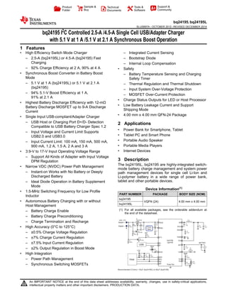
![bq24195, bq24195L
SLUSB97A –OCTOBER 2012–REVISED DECEMBER 2014 www.ti.com
Table of Contents
8.4 Device Functional Modes........................................ 251 Features.................................................................. 1
8.5 Register Map........................................................... 262 Applications ........................................................... 1
9 Application and Implementation ........................ 343 Description ............................................................. 1
9.1 Application Information............................................ 344 Revision History..................................................... 2
9.2 Typical Application .................................................. 34
5 Description (Continued)........................................ 3
10 Power Supply Recommendations ..................... 386 Pin Configuration and Functions......................... 4
11 Layout................................................................... 387 Specifications......................................................... 5
11.1 Layout Guidelines ................................................. 38
7.1 Absolute Maximum Ratings ...................................... 5
11.2 Layout Example .................................................... 39
7.2 ESD Ratings ............................................................ 5
12 Device and Documentation Support ................. 407.3 Recommended Operating Conditions....................... 5
12.1 Documentation Support ....................................... 407.4 Thermal Information.................................................. 6
12.2 Related Links ........................................................ 407.5 Electrical Characteristics........................................... 6
12.3 Trademarks........................................................... 407.6 Typical Characteristics.............................................. 9
12.4 Electrostatic Discharge Caution............................ 40
8 Detailed Description ............................................ 11
12.5 Glossary................................................................ 40
8.1 Overview ................................................................. 11
13 Mechanical, Packaging, and Orderable8.2 Functional Block Diagram ....................................... 11
Information ........................................................... 418.3 Feature Description................................................. 12
4 Revision History
Changes from Original (October 2012) to Revision A Page
• Added Handling Rating table, Feature Description section, Device Functional Modes, Application and
Implementation section, Power Supply Recommendations section, Layout section, Device and Documentation
Support section, and Mechanical, Packaging, and Orderable Information section. .............................................................. 1
• Changed VSLEEPZ, VBAT_DPL_HY, VBATGD , ICHG_20pct, VSHORT, IADPT_DPM, KILIM, VBTST_REFRESH in Electrical Characteristics.......... 6
• Added –40°C to 85° to IBAT Test Condition............................................................................................................................. 6
• Added REG00[6:3] = 0110 (4.36 V) or 1011 (4.76 V) to VINDPM_REG_ACC Test Conditions...................................................... 8
• Added a MIN value of 435 to KILIM.......................................................................................................................................... 8
• Deleted TJunction_REG MIN and MAX ......................................................................................................................................... 8
• Changed VOTG_ILIM to IOTG_ILIM ................................................................................................................................................. 9
• Changed Functional Block Diagram..................................................................................................................................... 11
• Changed Charging Current in Table 3 ................................................................................................................................. 17
• Changed REG09[5:4] to REG08[5:4] in Charging Termination section ............................................................................... 19
• Changed Charging Safety Timer description........................................................................................................................ 20
• Changed Host Mode and Default Mode description............................................................................................................. 25
• Changed Charge Current Control Register REG02 Bit 0 description and note ................................................................... 29
2 Submit Documentation Feedback Copyright © 2012–2014, Texas Instruments Incorporated
Product Folder Links: bq24195 bq24195L](data:image/gif;base64,R0lGODlhAQABAIAAAAAAAP///yH5BAEAAAAALAAAAAABAAEAAAIBRAA7)