Bhosari ( Call Girls ) Pune 6297143586 Hot Model With Sexy Bhabi Ready For ...
Module collection
1. 34 Everyday Practical Electronics, January 2018
IF YOU’VE been reading EPE for a
while now, you’ll have noticed that
small electronic modules have been
creeping into our projects.
These are not just Micromite, Ar-
duino or Raspberry Pi boards, but
really small and low-cost modules
including real-time clocks/calendars
(RTC), USB-to-UART serial ‘bridges’,
UHF data transmitters and receivers,
DDS signal generators, OLED/LCD
panels, touch-screen TFT LCDs, tem-
perature/humidity sensors, microSD
card interfaces and many more. They
seem to be breeding like rabbits!
Many of these modules have sprung
into life initially as ‘peripherals’ for
baby micros like the Arduino (ie,
shields) and Raspberry Pi. But most of
them have a lot of other applications
in circuits and designs using standard
TTL or CMOS ICs, and even in designs
using olde-worlde discrete transistors.
But the really big advantage of this
new generation of pre-built modules
is that most of them are surprisingly
low in cost. In fact, with many of them,
you’ll find that the cost of a complete
module is much less than the price
you’d pay for the main IC chip
used in them.
A prime example is the
popular real-time clock/
calendar module using
Maxim’s very accurate
DS3231 RTC chip — plus
a 24C32 4KB EEPROM,
in most cases. Although
the module is usually ad-
vertised as intended to be
used with an Arduino, it has
a standard I²C (‘Inter-IC’) in-
terface and can actually be used with
most other micros (we used it with
the Micromite in our Touchscreen
Super Clock).
So that’s the rationale behind
this series of articles on the new ‘el
cheapo’ modules. They’re readily
available, often have many applica-
tions and they’re usually much cheap-
er than building up the same circuits
for yourself. As a result, they’ve now
reached the status of being just stand-
ard circuit components. The Electron-
ic Modules As Components or ‘EMAC’
revolution has begun!
Let’s get the ball rolling by looking
at real-time clock/calendar modules.
RTC modules
Probably the first low-cost RTC mod-
ules to appear were those based on
the Philips/NXP PCF8563 chip, a low-
power 8-pin CMOS device which has
an I²C interface but needs an external
32.768kHz crystal. Modules based
on the PCF8563 are still available at
low cost from eBay or AliExpress,
but they tend to be less popular than
modules based on one of two newer
Maxim chips: either the DS1307 or
the DS3231.
Like the PCF8563, the DS1307
needs an external 32kHz crystal. How-
ever, it also has a built-in power sense
circuit which switches to a backup
battery when it detects a power fail-
ure. It has 56 bytes of internal non-
volatile SRAM and a standard I²C
interface, making it compatible with
just about every type of microcon-
troller module such as the Arduino
or the Micromite.
It does have one shortcoming,
though: the time-keeping accuracy
is inclined to drift a little with tem-
perature and so it can vary by a few
minutes a month.
Clock/calendar modules using
the DS1307 tend to cost more than
those using the PCF8563, but they
often include extras like a DS18B20
temperature sensor and a 24C32 se-
rial EEPROM (32Kbits = 4KB). This
makes them quite attractive for ap-
plications where extreme accuracy
isn’t too critical.
But modules based on the DS3231
chip are currently the most popular,
partly because the DS3231 has an on-
chip temperature-compensated crys-
tal oscillator and crystal.
It also includes an internal temper-
ature-compensated voltage reference
and comparator, both to maintain its
own supply voltage and to automati-
cally switch to a backup supply when
necessary.
These features allow it to provide
significantly higher timekeeping ac-
curacy: better than ±2ppm between 0
By JIM ROWE
The new standard
components!
Using Cheap Asian Electronic Modules Part 1
This is the first of a series of small articles which will help you take advantage of
the wide range of handy pre-built electronic modules that are now available from
Asia. This month, we review the DS3231 real-time clock (RTC), which is the per-
fect partner for popular microcontrollers like the Arduino or Micromite.
chip
e
as
c
p
c
t
a
a
o
c
n
s
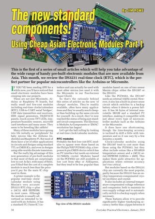
Top view of the DS3231 module
2. Everyday Practical Electronics, January 2018 35
and 40°C, or ±2 minutes per year for a
temperature range of –40°C to +85°C.
Its single shortcoming compared with
the DS1307 is that it lacks the internal
non-volatile SRAM.
Despite the advantages offered by
the DS3231, modules using it tend to
cost no more than those based on the
DS1307 or the PCF8563. And this ap-
plies for modules like the one shown
in the pictures, which also includes
a 24C32 serial EEPROM.
As mentioned earlier, this is the
RTC module that has been used in
a number of recent projects like the
Touchscreen Super Clock and the
Micromite Explore 100, so it’s the one
we’ll now concentrate on.
DS3231 RTC
As shown in the circuit diagram of
Fig.1, there isn’t a great deal in this
module apart from the DS3231 chip
itself (IC1), its 3.6V backup battery and
the 24C32 serial EEPROM (IC2). We’ll
discuss the rest of the components and
circuitry shortly after we’ve looked at
what’s inside the DS3231.
Its compact 16-pin small outline
(SO) SMD package contains an I²C data
bus interface, address decoding for
the 18 internal time, date and control
registers, a temperature sensor and a
power control circuit which can swing
over to the backup battery when the
supply voltage (VCC) fails. Its block
diagram is shown in Fig.2.
Then there’s a complete tempera-
ture-compensated 32.768kHz crystal
oscillator (TCXO), followed by a fre-
quency divider chain and all of the
time (seconds/minutes/hours), date
(day of week, day of month, month and
year), alarm, status and control reg-
isters. Finally, there’s reset circuitry
plus output buffers for both the 32kHz
TCXO oscillator and the square wave
output when it’s enabled.
Note that since the module tracks
the date as well as the time, it is more
correctly described as a real-time
clock and calendar (RTCC) module
but we’ll stick with the more com-
mon RTC term.
As well as the time and date reg-
isters, the DS3231 also provides two
time-of-day alarm functions which are
programmable via two sets of dedi-
cated registers. These can generate
an interrupt output signal via pin 3
(INT/SQW), for feeding directly back
to a micro.
When pin 3 is not being used to
provide this alarm interrupt function,
it can be used to provide square wave
timing signals derived from the 32kHz
TCXO. The square waves can be pro-
grammed for one of four frequencies:
1Hz, 1.024kHz, 4.096kHz or 8.192kHz.
These are in addition to the 32.768kHz
signal made available at pin 1.
All of the DS3231’s function set-
tings, along with the initial time and
date, can be programmed using the I²C
bus to write into the appropriate inter-
nal registers. Then the time, date and
status can be subsequently obtained
by using the I²C bus to read from the
same registers.
Pins 15 and 16 of the device are
used for the I²C bus connections: pin
15 for the SDA serial data line and pin
16 for the SCL serial clock line. On the
module shown, these are both pro-
vided with surface-mount 4.7kȍ pull-
up resistors to VCC, as are pin 1, the
32.768kHz output and pin 3, the INT/
squarewave output. (The latter two
pins are open-drain outputs, so they
need the external pull-up resistors.)
That’s probably about all you need
to know about the DS3231 itself, apart
from the way that pin 14 (VBAT) is used
for the connection to the 3.6V lithium-
ion rechargeable backup battery. In the
module shown here, diode D1 and its
series 200ȍ resistor are used to main-
tain the battery charge when VCC is
connected to the module. LED1 and
its series 1kȍ resistor are used to pro-
vide a power-on indicator. We’ll have
more to say about battery options later.
Note the two I/O headers, labelled
in Fig.1 as CON1 and CON2. CON1
provides pins for both the 32kHz
and SQW/INT outputs, as well as the
SCL/SDA/VCC/GND bus connections,
while CON2 provides only the latter
four connections, essentially to allow
daisy-chaining further devices to the
I²C bus – additional memory chips,
for example.
Now let’s look at IC2, the 24C32
serial EEPROM chip, which is some-
thing of a bonus. The 24C32 is a 4KB
(32Kb) device, with a standard I²C
serial interface. In this module, the
SDA line (pin 5) and SCL line (pin 6)
are connected in parallel with those
for IC1, to the module’s SDA and SCL
lines at both CON1 and CON2.
To allow IC2 to be addressed by
the micro without conflicting with
commands or data sent to or received
from IC1, it has a different slave
address on the I²C bus. In fact, it
can have any of eight different slave
VBAT
Vcc
NC GND
SCL
SDA
RST
INT SQW/
32kHz
1
2
3
4
5–12 13
14
15
16
IC1
3231DS
IC1
3231DS
AA
KK
32k
SQW
SCL
SCL
SDA
SDA
VCC
VCC
GND
GND
4x
4.7k
4x
4.7k
100nF 10 F 1k200
LED1
D1
1N4148
3.6V
-LI ION
BATTERY
( )RECHARGEABLE
SDA
SCL
Vss
Vdd
A0
A1
A2
NC
IC2
24C 23
IC2
24C 23
1
2
3
4
5
6
7
8
A0 A2A1
CON1
CON2
(TO SET SLAVE
2)ADDRESS OF IC
I C ( ) 24C32SLAVE ADDRESSES HEX FOR EEPROM
MSD FIXED( ) A2 A1 A0 WRITE READ
A
A
A
A
A
A
A
A
1
1
1
1
0
0
0
0
1
1
0
0
1
1
0
0
1
0
1
0
1
0
1
0
2
AE
AC
AA
A8
A6
A4
A2
A0
AF
AD
AB
A9
A7
A5
A3
A1
DEFAULT ADDRESS
(NO LINKS ON PADS
A0, A1 A2)FOR OR
NOTE SLAVE: I C
3231ADDRESS FOR DS IS
D0 ( ) ,HEX FOR WRITING
D1 ( )HEX FOR READING
2
1 0 1 0 A2 A1 A0
R
W
24C32 ADDRESS BYTE FORMAT
FIXED
SET BY
LINKS
Fig.1: complete circuit for the DS3231-based RTC module. Both CON1 and CON2
provide serial bus and power connections, allowing extra devices to be connected.
Note that the I2C bus should have only one set of pull-up resistors.
3. 36 Everyday Practical Electronics, January 2018
addresses, as set by the voltage levels
of pins 1, 2 and 3 (labelled A0, A1
and A2).
As shown in Fig.1, the module pulls
all three pins up to VCC via the 4.7kȍ
resistors by default, which gives IC2 a
slave address of AE/AF hex (AEh for
writing, AFh for reading). But it also
provides three pairs of pads on the
PCB so that any of the three address
pins can be pulled low (to ground)
by soldering across the A0, A1 or A2
pads. This allows the slave address
of IC2 to be set to any of the eight
possible values, as shown.
So since the slave address of IC1
(the DS3231) is fixed at D0/1 hex (D0
for writing, D1 for reading), there is
no conflict. In fact, the main reason
for changing the slave address of IC2
via the wire links would be to avoid
a conflict with any other devices that
may be attached to the I²C bus.
How it’s used
Since both the DS3231 and 24C32
devices on the module are
intended for
use via the I²C bus, this makes it easy
to use with any micro or other system
provided with at least one I²C inter-
face. (Even if you don’t have such an
interface, you can use two GPIO pins
in ‘bit banging’ mode, but that’s out-
side the scope of this article.)
For example, to use it with an Ar-
duino Uno or similar all you need
to do is connect the SCL line on the
module to the AD5/SCL pin on the Ar-
duino, the SDA line to the AD4/SDA
pin, the VCC pin to the +5V pin and
the GND pin to one of the Arduino’s
GND pins.
It’s just as easy with the Micromite.
In this case, the SCL pin connects to
pin 17 on the Micromite’s main I/O
pin strip, while the SDA pin connects
to pin 18 next to it. Then the VCC and
GND pins connect to the +5V pin and
GND pins on the same pin strip.
Programming either of the chips
on the module should also be fairly
straightforward, because of the I2C
interfacing. The main thing to re-
member is that I2C transactions
always begin with a control
byte sent by the master (the mi-
crocontroller), specifying the
address of the slave device it
wishes to communicate with
and whether it wants to write
to or read from the device.
So, for example, the con-
trol byte to initiate a write
operation to one of the registers in
the DS3231 would be D0h, while the
control byte to read from one of the
addresses in the 24C32 would be AFh
(assuming it’s at the default address
on your module).
After the slave device sends back
an ‘ACK’ or acknowledge indication
(to show that it’s present and ready
for a transaction), the micro then
sends the address of the register or
memory location in the device that it
wants to write data to or read it from.
When this has been acknowledged,
the actual write or read transactions
can take place.
If this sounds a bit complicated,
you’ll be relieved to hear that if you’re
using one of the popular micros like
the Arduino or Micromite, you prob-
ably don’t need to worry about this
yourself. That’s because this has usu-
ally been taken care of in small code
libraries, with functions specifically
written for I²C data communications.
In the case of the Micromite, in fact,
I²C communication is handled by the
MMBASIC interpreter.
For example, if you are using an
Arduino, the Arduino IDE application
already includes a ‘Wire’ library, pro-
viding about nine different functions
for passing data between the micro
and an I²C device.
Similarly, if you’re using a Micro-
mite, you’ll find that Geoff Graham’s
MMBASIC already includes functions
like RTC SETTIME, RTC GETTIME,
RTC SETREG and RTC GETREG spe-
cifically for talking to the DS1307 or
DS3231 RTC devices. And there are
other functions like I2C OPEN, I2C
WRITE, I2C READ and I2C CLOSE
for data transactions with other I2C
devices (like the 24C32 EEPROM chip
in the current module).
Finally, there’s also an automatic
variable called MM.I2C, which can be
read after any I2C transaction to find
out the result status.
So all in all, the RTC module shown
with its DS3231 clock/calendar chip
(and bonus 24C32 EEPROM chip) is
relatively easy to use, and exceptional
value for money.
Here is a link to a useful web tutorial
by John Boxall of tronixlabs, explain-
ing how to use either the DS1307 or
DS3231 RTC modules with an Ardui-
no: http://bit.ly/2yTbIWy
Final note: this module has onboard
pull-up resistors for the I²C bus, you
may need to remove them, or avoid fit-
ting pull-up resistors on the master, for
it to share a bus with other peripherals.
CLOCK AND CALENDAR
REGISTERS
USER BUFFER
(7 BYTES)
VOLTAGE REFERENCE;
DEBOUNCE CIRCUIT;
PUSHBUTTON RESET
I C INTERFACE AND2
ADDRESS REGISTER
DECODE
POWER CONTROL
V
V
GND
CC
BAT
SCL
SDA
TEMPERATURE
SENSOR
CONTROL LOGIC/
DIVIDER
ALARM, STATUS, AND
CONTROL REGISTERS
OSCILLATOR AND
CAPACITOR ARRAY
X1
X2
N
32kHz
N
INT SQW/
SQUARE-WAVE BUFFER;
INT/SQW CONTROL
N
RST
VCC
DS3231
1Hz
1Hz
Fig.2: block diagram for the DS3231. A comparator monitors both VCC and VBAT
and the DS3231 is powered from whichever is higher. The oscillator is automatically
temperature-compensated for accuracy.
Rear view of the DS3231 module showing
the 3.6V Li-ion backup battery (pin 14) which
powers the real time clock when the supply voltage (VCC) fails.
devices on the module are
intended for
mem
alw
by
cr
ad
w
a
t
Rear view of
the 3.6V Li-ion b
Reproduced by arrangement
with SILICON CHIP
magazine 2017.
www.siliconchip.com.au
4. 1 www.handsontec.com
Handson Technology
Data Specs
DS3231 High Precision Real Time Clock
DS3231 is a low cost and extremely accurate I2C real-time clock, with an integrated crystal
and temperature-compensated crystal oscillator (TCXO). DS3231 can be operated using
supply voltages ranging from 2.3V to 5.5V and it also features battery backup capabilities.
The on-board AT24C32 32KB EEPROM that can be used to add non-volatile data storage to
your electronic projects and prototypes.
SKU: MDU-1036
Brief Data:
Standard 2.54mm pins pitch for input and output connections.
Two programmable square-wave outputs.
Backup battery socket compatible with CR2032 3V Lithium batteries.
Clock accuracy: ±2ppm.
32KB EEPROM Memory chip: AT24C32.
On-chip temperature sensor with an accuracy of ±3℃.
I2C bus interface maximum speed: 400kHz.
Small Size: 38 x 22 x 14 mm.
5. 28 Everyday Practical Electronics, March 2018
IF THE HC-SR04 module shown in
the picture looks familiar, that’s be-
cause it has already been used in Geoff
Graham’s Ultrasonic Garage Parking
Assistant,publishedintheJune2017is-
sue. But this module doesn’t have to be
usedwithamicroprocessormodulelike
a Micromite or an Arduino, it can also
be used with much simpler circuitry.
Before we get to how it works, we
should note that these ultrasonic sen-
sor modules have been around for
about six years, beginning life as an
add-on ‘shield’ for the Arduino. Since
then, they have gone through a num-
ber of iterations, all bearing the same
HC-SR04 label but with various minor
circuit and component changes. We
suspect this has been due to various
manufacturers working out ways of
reducing costs, rather than seeking to
achieve better performance.
The bottom line is that although
some of these slightly different HC-
SR04 modules are still being sold,
they all seem to function and perform
much the same. So don’t worry if the
module you buy looks a little different
from that shown in the photos. The
odds are that if your module carries
the label HC-SR04, it will work just
like any other HC-SR04.
Current HC-SR04 modules are based
on a PCB measuring 45 × 20mm. On
the top side of the PCB is a pair of small
(16mm diameter) ultrasonic transduc-
ers with a 4MHz crystal between them.
All the components on the other
side of the PCB are surface-mount
types, apart from the 4-pin right-angle
header at bottom centre. Fig.1 shows
how it’s used. It sends out a burst of
ultrasonic energy from the transmit-
ter transducer (the one marked T, on
the left) and then listens via the other
receiver transducer (marked R, on the
right) for any echo that may be reflect-
ed back from an object in front of the
module (see Fig.1).
If it detects this ultrasonic echo,
it produces an output pulse with a
width approximately proportional
to the distance between the mod-
ule’s sensors and the object produc-
ing the echo.
The ultrasonic frequency used is
very close to 40kHz, roughly double
By JIM ROWE
The HC-SR04
Ultrasonic Distance
Sensor Module
In the second article on cheap pre-built electronics modules, we’re
focusing on the HC-SR04 ultrasonic distance sensor module. We
describe how the module works and show how it can be used as a
hallway monitor or door sentry.
≈
Fig.1: one ultrasonic burst is sent out from the transmitter
transducer. The receiver transducer will detect this burst if it
is reflected off an object in front of the module. Once detected
by the receiver, an output pulse is produced with a width in
microseconds of (distance in cm) ÷ 0.01725.
Fig.2: there must be a delay of 60ms between trigger pulses
to prevent late echoes from affecting successive readings.
Using Cheap Asian
Electronic Modules Part 2
6. Everyday Practical Electronics, March 2018 29
the highest frequency that can be heard
by human ears. The burst of transmit-
ted energy consists of eight pulses at
40kHz, so the transmitted burst lasts
for only 200μs, as shown in Fig.2.
Since the speed of sound in air at
25°C and 100kPa (ie, 1 bar) is close to
345m/s (= 0.0345cm/μs) and the dis-
tance travelled by the ultrasonic burst
energy corresponds to double the dis-
tance between the transducers and the
reflecting object, we can calculate the
distance from the delay as follows:
distance in cm =
0.0345 x echo pulse width (μs)
2
= 0.01725 x echo pulse width (μs)
As shown in Fig.2, each measurement
cycle begins when a positive trigger
pulse of at least 10μs duration is ap-
plied to the HC-SR04 module’s trigger
input pin. When the echo has been
detected, it then produces a pulse at
the echo output pin. Note that there
should be at least 60ms between trig-
ger pulses, to prevent late echoes from
one cycle causing false readings on the
next. So in practice, it’s a good idea to
limit the trigger pulse frequency to no
more than 16Hz.
Circuit details
The full circuit for the HC-SR04 mod-
ule is shown in Fig.3. It is based on an
EM78P153S microcontroller (IC1), a
low-power 8-bit CMOS device made
by Elan Microelectronics in Hsinchu,
Taiwan. This device has a 1024 × 13
bits one-time programmable (OTP)
ROM plus 32 bytes of on-chip SRAM,
and comes in a 14-pin SOIC package.
It runs here with a 4MHz crystal be-
tween pins 5 and 6.
When a TRIG pulse arrives at pin 1
of IC1 (from pin 3 of CON1), the con-
troller generates a 40kHz burst signal
of eight pulses at pins 13 and 14, with
one pin 180° out of phase with the
other. These go to pins 10 and 11 of
IC3, a bus driver IC very similar to the
MAX232. The outputs from IC3 (pins
7 and 14) connect across the transmit-
ter transducer, effectively driving it
in bridge mode to emit the bursts of
ultrasonic energy.
Echoes picked up by the receive
transducer pass through the four sec-
tions of IC2, an LM324 quad op amp.
These provide amplification, band-
pass filtering and phase detection,
with the result that a received echo
pulse is fed back to pin 10 of IC1.
The micro then compares the timing
of the leading edge of this received
echo pulse with the leading edge of
the transmitted burst fed to IC3 and
the transmit transducer, and produces
an echo output pulse at pin 2 with its
width equal to the time difference.
This echo output pulse appears at
pin 2 of CON1.
How it’s used
If you want to use the HC-SR04 mod-
ule to actually measure the distance
to an object or wall in front of it, the
best way to do it is to hook it up to
a microprocessor module like an Ar-
duino, Micromite or Raspberry Pi. The
micro’s program generates the trigger
pulse to the HC-SR04, then measures
the length of the echo pulse and cal-
culates the corresponding distance.
There’s no need to worry about
writing a program to do these tasks
for you, because many people have
already produced programs to do this.
A quick search on the Arduino website
(www.arduino.cc) or by using Google
will find a sample program for the
micro you’re using in short order.
If you want to use the HC-SR04 with
a Micromite, Geoff Graham has already
built a DISTANCE function into his
MMBasic programming language for
the Micromite family to make it re-
ally easy.
W
W
W
W
W
W
W W
W
W W
W
W
W
W
W
W
Fig.3: complete circuit diagram for the HC-SR04 ultrasonic sensor module. When IC1 detects a TRIG pulse at pin 1, a
40kHz burst signal of eight pulses is generated at pins 13 and 14 of IC1. This is taken to pins 10 and 11 of IC3 respectively,
and output at pins 7 and 14 connecting to the transmit transducer.
7. Everyday Practical Electronics, March 2018
All you have to do to get the Micro-
mite to trigger the HC-SR04 and then
calculate the object distance from the
echo pulse is use this one-line func-
tion call:
d = DISTANCE(trig, echo)
Where ‘d’ is the distance in centime-
tres, ‘trig’ is the Micromite’s I/O pin
connected to the HC-SR04’s trigger
input pin and ‘echo’ is the I/O pin
connected to the HC-SR04’s echo out-
put pin.
The only extra step is to connect the
HC-SR04’s +5V and GND pins to the
corresponding pins of your Micromite.
If you want to display the result ‘d’
on an alphanumeric LCD, you can do
this using commands like:
LCD INIT ...
LCD 1, 2, “Distance = “
LCD 2, 6, STR$(d)
and so on.
You can get a good idea of what’s in-
volved in using the HC-SR04 with a
Micromite from Geoff Graham’s arti-
cle describing the Ultrasonic Garage
Parking Assistant.
But say you want to use this mod-
ule without a microcontroller at all.
That’s fairly straightforward, as we’ll
now demonstrate.
A simple intruder alarm
For example, to use it as an ultrason-
ic intruder alarm, have a look at the
circuit shown in Fig.4. It uses three
low-cost CMOS ICs, a 2N7000 MOS-
FET, three diodes, one LED, a piezo
buzzer and some passive components.
This circuit and the HC-SR04 operate
from a common 5V DC power supply,
which can be from a USB plugpack or
USB power bank.
IC1 is a hex Schmitt trigger invert-
er package and we’re using just two
sections of it, IC1a and IC1b. IC1a at
upper left is connected as a relaxa-
tion oscillator, to generate a stream
of 60μs-wide pulses at a frequency of
about 12Hz, ie, with a pulse spacing
of about 83ms. These form the trigger
pulses, which are fed to the HC-SR04
via pin 3 of CON1.
The rest of the circuit monitors the
widthoftheechopulsessentbackfrom
the HC-SR04 via pin 2 of CON1. If this
varies significantly (indicating that
something has moved between the sen-
sor and the nearest object, like the op-
positewallofyourentryhall),itsounds
thealarmbyswitchingonLED1andthe
piezo buzzer connected across it.
This section is a little more com-
plex. First, the incoming echo pulse
passes through inverter IC1d, so that
its leading edge is negative-going. The
1nF capacitor and 100kȍ resistor then
form a differentiator circuit, which de-
velops a narrow negative-going pulse
from the negative-going leading edge
of the inverted pulse.
This is then used to trigger IC2, a
7555 CMOS timer chip connected as
a one-shot multivibrator. When IC2
is triggered, its output pin 3 switches
high for a short time, determined by
the 2.2μF capacitor connected from
pins 6 and 7 to ground and the resist-
ance connected between the same two
pins and the +5V line.
As shown, this resistance is the
series combination of a 10kȍ resistor
and VR1, a 100kȍ pot. So by varying
VR1, we can vary the width of the
pulse generated each time the one-
shot is triggered.
The output of IC2 is connected to
pin 2 of IC3a, one section of a 4070B
quad XOR (exclusive-OR) gate. The
echo pulses from the HC-SR04 are fed
to pin 1 of IC3, the second input of the
same XOR gate. Since the output of
an XOR gate is high only when one of
its inputs is high and the other low, it
forms a pulse-width comparator.
Consider the situation where the
HC-SR04 sensor is facing a wall, say
1.5m or 150cm away. The echo pulses
fed back from the sensor will be very
close to 8.7ms wide and these are fed
to input pin 1 of IC3a.
If we adjust VR1 so that IC2 also
produces 8.7ms-wide pulses, then
since they start at virtually the same
instant at the start of the echo pulse,
both inputs of XOR gate IC3a will rise
and fall at the same time. As a result,
the output of IC3a (pin 3) will remain
low at all times.
Fig.4: complete circuit for an ultrasonic intruder alarm using an HC-SR04 module. IC1a generates 60μs-wide trigger pulses
at 12Hz, which are fed to pin 3 of CON1. The echo pulses trigger monostable multivibrator IC2, and IC3a then compares
the width of the resulting pulse to the echo pulse. If these differ, LED1 lights and the piezo buzzer sounds.
This tiny active piezo transducer
module from Jaycar can be used in
the intruder alarm instead of the
piezo buzzer.
8. Everyday Practical Electronics, March 2018
But if someone moves in front of
the HC-SR04, this will cause the echo
pulses to shorten, because the ultra-
sonic energy reflected back by the
person or object will be travelling over
a smaller distance. So the echo pulse
width will drop briefly to say 5-6ms,
and as a result the inputs of IC3a will
no longer be synchronised.
Although the pulses fed to pin 2 will
still be high for 8.7ms, the echo pulses
being fed to pin 1 will drop low after
5-6ms, so the output of IC3a will switch
highfortheremaining2.7-3.7ms.These
positive-going pulses will very quickly
charge up the 1μF capacitor in the gate
circuit of MOSFET Q1, via diode D3
and the 10kȍ series resistor, and this
will turn on Q1, causing LED1 to light
andthepiezobuzzertosoundthealarm.
Then, when the intruding person
or object moves away again and the
echo pulses return to their original
width of 8.7ms, the pulses fed to the
two inputs of IC3a will be again be
synchronised. There will be no more
output pulses from IC3a and the 1μF
capacitor will be discharged by the
1Mȍ resistor connected across it. So
within a couple of seconds, the buzzer
and LED will switch off.
The circuit is quite easy to set up,
too. All you need to do is wire it up
and connect it to the HC-SR04 module
using a suitable length of 4-conductor
cable. Then mount the sensor module
on one side of the hall or doorway
you want to monitor, facing either a
wall or a large fixed object such as a
dresser, a chest of drawers or a filing
cabinet.
Next, set pot VR1 to its fully anti-
clockwise (ie, minimum resistance)
position and turn on the 5V power
supply. You’ll find that LED1 will
immediately light, and if you have
a piezo buzzer connected as well, it
will sound. That’s because the pulses
being generated by the one-shot IC2
will be shorter than the echo pulses
coming from the HC-SR04.
Now slowly turn pot VR1 clockwise
until LED1 turns off and the piezo
buzzer goes silent. Your intruder
alarm will then be set up and ready
to detect the presence of a ‘foreign
body’ in the space between the sen-
sor and its reflecting wall. So we’ve
done all this without a microproces-
sor – apart from the EM78P153S micro
inside the HC-SR04 sensor module
itself, of course.
1 HC R0 ult asonic senso
1 acti e pie o t ansduce module OR
1 pie o u e
1 100 ȍ t impot ( R1)
Semiconductors
1 1 819 diode ( 1)
2 1 1 8 diodes ( 2)
1 E an colou ( E 1)
1 2 000 M E ( 1)
1 010 o HC1 CM C ( C1)
1 M CM time C ( C2)
1 0 0 uad R ate C ( C3)
Capacitors (16V)
1 2.2
1 1
2 100n
1 1n
Resistors (0.25W, 5%)
1 2.2Mȍ 1 1Mȍ 1 100 ȍ
2 10 ȍ 1 1. ȍ 1 0ȍ
1 100ȍ
Parts List
Reproduced by arrangement
with SILICON CHIP
magazine 2018.
www.siliconchip.com.au
e t oni 30 2 /C
e t oni 3032
e t oni 3012
e t oni 2 30A
e t oni 2
a nell AP 0/ 0
a nell H 0/ 0
a nell A3 /2
a nell 1
Racal 1991
Racal 2101
Racal 9300
Racal 9300
lu e 9
lu e 99
i at onics 100
ea a d o a
ola t on 1 0/P
olat on 12 3
asa a o M03 2
hu l P 320 M
hu l 210
HP33120A
HP 3131A
HP 3131A
scilloscope 00MH 2. /
scilloscope 300MH 2. /
scilloscope 2 Channel 100MH 1.2 /
scilloscope ual ace 1 0MH 100M /
scilloscope Channel 00MH
P 0 0 0 0A 1 itch Mode
P 0 0 0 0A
P 0 3 0 2A ice i ital
ine/s scillato 10H 1MH
Counte / ime 1 0MH 9 i it
Counte 20 H E
ue RM Milli oltmete H 20MH etc
As 9300
copemete 2 Channel 0MH 2 M /
copemete 2 Channel 100MH /
nthesised i nal ene ato 10MH 20 H
PA este
1/2 i it MM ue RM EEE
ain Phase Anal se 1mH 20 H
P 0 3 0 2A 2 Mete s
P 0 30 0 2A ice
unction ene ato 0.002 2MH etc en ood ad ed
unction ene ato 100 mic oH 1 MH
ni e sal Counte 3 H o ed unused
ni e sal Counte 22 MH
1 00
99
0
3 0
00
19
00
1 0
29
12
1 9 0
9
/
00
30
1 0 200
2 0 300
00
3 0
STEWART OF READING
1 A in t eet Mo time nea Readin R 3R
elephone: 0118 933 1111 a : 0118 9331275
E E EC R C E E PME
Chec e site www.stewart-of-reading.co.uk
(ALL PRICES PLUS CARRIAGE & VAT)
Please check availability before ordering or calling in
AM A E E
AM A E E
R 202
Ma coni 29
R AP 2
HP332 A
HP3 1A
HP 032A
HP 22A
HP 2 A
HP 32
HP A
HP A
HP83 1A
HP83 31A
HP8 8 A
HP8 0A
HP8 0E
HP8 3A
HP8
HP8 2A
Ma coni 2022E
Ma coni 202
Ma coni 2030
Ma coni 230
Ma coni 2 0
Ma coni 29 /A/
Ma coni 29
Ma coni 29 A
Ma coni 200
Ma coni 200A
Ma coni 200
Ma coni 9 0 ith
P E 100 1 100 1 A o ed As e
P E 0 30 0 30A
i nal ene ato 9 H 2. 1 H pt 0 /11
Radio Communications est et
n unction ene ato 1H 2 0 H
nthesised unction ene ato
namic i nal Anal se
P 0 0 0 0A 1000
P 0 20 A ice o 0 0 2A ice
P utputs
P 0 20 0 A
P 0 0 3. A
P 0 0 0 9A
nthesised eep ene ato 10MH 20 H
nthesised i nal ene ato 1 20 H
Po e enso 0.01 18 H 3n 10u
pect um Anal se nthesised 0H 2.9 H
pect um Anal se nthesised 30H 2.9 H
pect um Anal se nthesised 9 H 22 H
pect um Anals e 100H 22 H
R ene ato 10 H 1280MH
nthesised AM/ M i nal ene ato 10 H 1.01 H
nthesised i nal ene ato 9 H 2. H
nthesised i nal ene ato 10 H 1.3 H
Modulation Mete
Counte 20 H
Communications est et a ious ptions
Radio Communications est et
Radio Communications est et
Mic o a e est et
Mic o a e est et 10MH 20 H
Mic o a e est et
910 Po e Mete
32
32
900
800
19
19
0
0
3 0
3 0
19
00
00
2 000
1 800
1 2 0
1 0
2 2 0
1 200
0
32
800
0
2 0
29
3 0
9
2
1 00
1 9 0
2 300
29
2 000 –
FANTASTIC MODERN POWER SUPPLY ONLY IU
HIGH PROGRAMMABLE
CA E PP E H P A
RA CA E
PR PER 200MH
A A E C PE 2 0
R A AR MM
32 R 2 H HA E
A MPER
E A HP 100MH C PE R
R C MP E E H A
ACCE R E 12
800
9. 1 www.handsontec.com
Handson Technology
User Guide
HC-SR04 Ultrasonic Sensor Module
HC-SR04 Ultrasonic Sensor is a very affordable proximity/distance sensor that has been
used mainly for object avoidance in various robotics projects. It has also been used in turret
applications, water level sensing, and even as a parking sensor.
SKU: SSR-1012
Brief Data:
Power Supply: 3.3~5 VDC
Quiescent Current : <2mA
Working Current: 2.8mA @ 5V
Effective Angle: <15°
Ranging Distance : 2cm – 400 cm or 1″ – 13ft
Connector: 4-pins header with 2.54mm pitch.
Dimension: 45mm x 20mm x 15mm
Weight 8.5-g.
10. 2 Everyday Practical Electronics, March 2018
THE SECOND MODULE we’re looking
at this month has been used in a
number of recent projects. It’s a serial
USB-UART (universal asynchronous
receiver/transmitter) bridge which al-
lows just about any microcomputer or
peripheral module to exchange data
with a PC, via a standard USB port.
Let’s start by explaining what is
meant by the rather clumsy term’serial
USB-UART bridge’. First, a UART is
an interface which can operate in one
of several different common serial
protocols. The serial protocol we’re
most interested in (and which is most
widely used) is 3.3V ‘TTL’ RS-232. The
term ‘bridge’ simply refers to the fact
that this module allows data to pass
between the USB interface and UART
interface unchanged.
In fact, we’ve already described
a device with essentially the same
purpose, the Microchip MCP2200
‘protocol converter’ used in the USB/
RS-232C Serial Interface which was
published in the April 2015 issue.
Note that for a UART to provide a
fully compatible RS-232 serial port,
as used in many now-obsolete PCs,
it’s necessary to provide level shifting
from the UART’s 3.3V (TTL) signal-
ling levels to the RS-232 bipolar logic
levels of ±3-15V.
But these days, RS-232 is commonly
used for short-range communications
between microcontrollers and bridges
and in this case, the TTL signal levels
are all you really need.
The first serial USB-UART bridge
modulestobecomepopularwerebased
around British firm FTDI’s improved
FT232R converter chips. However,
these chips became so popular that
some Asian firms made ‘clones’ of
them, even going so far as copying the
package markings.
Understandably, this upset FTDI
and as a result they released a new
version of their Windows VCP driver
which was able to identify when a
clone chip was being used and dis-
able it. This ‘clone killer’ driver was
included in an automatic update that
Microsoft unwittingly provided to
Windows users.
As a result, thousands of people
found that their low-cost USB-UART
converter modules, some inside com-
mercial products, suddenly stopped
working and became worthless. Natu-
rally, this made many people cautious
of buying any converter based on the
FTDI FT232R chip, because of the diffi-
culty in ensuring that you are buying a
genuine FTDI chip rather than a clone
chip that would stop working as soon
as you tried to use it with Windows.
As a result of this, CP2102-based
USB-UART bridges have become very
popular. These are not only less expen-
sive than FT232-based modules but are
(currently)freefromsuchdriverissues.
A good example of this type of mod-
ule is the tiny one shown in the photo
to the right. This same module has
been used in recent projects and can
be used with virtually any Micromite
to program the micro as well as debug
the software or load data into or out of
the micro’s RAM.
The CP2102-based bridge
As you can see from the photo and cir-
cuit diagram in Fig.1, there’s very little
in this module apart from the CP2102
chip (IC1), three indicator LEDs and
half a dozen passive components.
The internals of IC1’s tiny (5 × 5mm)
28-pin QFN SMD package are shown
in the internal block diagram, Fig.2.
It’s conceptually quite simple but in-
volves tens of thousands of logic gates
and memory cells as well as carefully
designed analogue circuitry.
The main functional blocks are the
USB transceiver at lower left, the USB
function controller at lower centre and
the UART block at lower right with its
full range of data and handshaking in-
puts and outputs. Notice that there’s
also an internal 1024-byte EEPROM
A CP2102 module, measuring only 20 ×
16mm. Two of the indicator LEDs glow
when data is being transmitted.
Computer
Interface Modules
Computer
Interface Modules
Want to connect a microcontroller to your PC? How about interfacing
with a microSD memory card? These low-cost modules make life
really easy! Jim Rowe shows you how.
Using Cheap Asian
Electronic Modules Part 3
11. Everyday Practical Electronics, March 2018
used to store the USB ID information:
the vendor ID, the product ID, the se-
rial number, the power descriptor, the
release number and product descrip-
tion strings.
In addition, there are two RAM buff-
ers, one 640-byte USB transmit buffer
and one 576-byte USB receive buffer.
Since the CP2102 has a calibrated
48MHz oscillator, it needs no exter-
nal crystal to operate at the USB 2.0
full-speed rate of 12Mbps. Finally, it
contains its own low drop-out (LDO)
voltage regulator, to give an output
of 3.3-3.45V from an input (REGIN)
within the range 4.0-5.25V. This means
that it can be powered directly from
the USB VBUS line.
Circuit details
While this regulator can supply up to
100mA, the circuitry within the chip
itself draws only a little over 26mA
(maximum) even in normal operation,
and only 100PA when suspended.
This means it can supply up to 70mA
or so for external circuitry needing a
3.3V supply.
In short, the CP2102 is a very im-
pressive chip. Now turn your attention
back to the module’s circuit of Fig.1.
There’s a micro-USB socket at the
left (CON1) to connect to a PC’s USB
port via a standard cable and also to
power the module itself. So the VBUS
line from pin 1 of the socket connects
to pins 7, 8 and 9 of the CP2102, with
10PF and 100nF bypass capacitors.
Note that the module does not pro-
vide connections to any of the CP2102
UART’s handshaking lines, except for
DTR (‘data terminal ready’). However,
this is unlikely to pose a problem for
most applications nowadays, since
even the DTR line is rarely used.
On the right-hand side there’s a
6-way pin header (CON2) for the
UART input, output and handshaking
(DTR) connections, plus the ground,
+5V and +3.3V power connections for
use by external circuitry. There’s also
a 100nF bypass capacitor on the +3.3V
line, plus three small indicator LEDs,
each with its own series resistor for
current limiting.
LED1 is driven from pin 11 of the
CP2102, the SUSPEND output, so it
only glows when the device is not sus-
pended by the host PC, ie, when it’s
communicating with the PC normally
via USB. On the other hand, LED2
and LED3 are connected between the
+3.3V supply (pin 6) and pins 26 (TXD)
and 25 (RXD) respectively, to indicate
when data is being sent and received
via the bridge.
LED1 draws a little over 1mA when
it’s operating, while LED2 and LED3
will each draw about 5mA. Thus the
LEDs could draw up to 11mA from the
3.3V supply (with full duplex serial
communications, allowing LED2 and
LED3 to light simultaneously) and this
should be taken into account when fig-
uring out how much reserve current is
available for external circuitry.
How to use it
Using the CP2102 based USB-UART
bridge module is very straightfor-
ward. But before you can do so, you
may need to install a virtual COM port
(VCP) driver on your PC. This is the
software which takes care of buffer-
ing data to and from the bridge and
setting up the UART. In Windows, it
makes the UART appear as if it were
a legacy COM port.
You can get the right VCP driver
from the Silicon Labs website: www.
silabs.com/products/interface/Pages/
interface-software.aspx
You can also download the latest
version of the CP2102 data sheet from:
www.silabs.com/support/Pages/docu-
ment-library.aspx
When you go there you’ll find they
can provide VCP drivers for not only
Windows 7-10, but also for Windows
2000/XP/Vista/Server 2003, WinCE,
Mac OS 9 and X, Linux (3.x.x and
2.6.x) and Android. They can also pro-
vide drivers for direct ‘USB-Xpress’
interfacing to the PC, as an alternative
to using the VCP approach.
Note that most modern operating
systems, including Windows 10 and
the latest versions of Mac OS X and
Linux, should already have a suitable
VCP driver installed. In this case, all
you need to do is plug the bridge into
a USB port and check that it has been
recognised (eg, in Windows, check that
a new COM port appears).
Once the driver is installed and
working, you can set up your applica-
tions to communicate with the module
via the new COM port. That includes
setting the correct baud rate and other
options.
Of course, your circuitry on the
UART side of the module needs to be
connected to the appropriate pins on
header CON2. These will usually be
just the RXI, TXO and GND pins, al-
though you might also want to make
use of one of the power supply pins
as well.
If you aren’t sure whether the bridge
is working properly, the simplest way
to test it is to wire up the RXI pin to
the TXO pin. You can then open a ter-
minal emulator, connect to that port
Fig.1: complete circuit diagram for the CP2102-based serial USB-UART bridge. The
CP2102 can be powered directly from the USB VBUS line and it contains a low drop-
out voltage regulator to provide 3.3-3.45V (VDD) from 4-5.25V (REGIN).
Fig.2: block diagram for
the CP2102. This UART
interface implements all
RS-232 signals, including
those for control and
handshaking, although
an external level shifter is
required for full RS-232
compatibility.
Reproduced by arrangement
with SILICON CHIP
magazine 2018.
www.siliconchip.com.au
12. Everyday Practical Electronics, March 2018
and type on your keyboard. The typed
characters should be sent back to you
and appear in the terminal. If that
works, but you still can’t communicate
with your target device, check that the
connections to its TX/RX pins are not
swapped and also that you have set the
right baud rate.
microSD card interface
There are many different adaptors for
accessing an SD memory card from a
microcontroller or embedded module
but they generally function in the same
manner. The main differences are in
terms of the card socket they provide
and the chip(s) they use for interfacing.
The full circuit for this module
is shown in Fig.3. Note that all SD
cards can communicate via either
serial peripheral interface (SPI) or a
faster method, which consists of ei-
ther a 4-bit parallel bus (older cards)
or a high-speed differential interface
(UHS-compatible cards). The SPI
method is by far the simplest to imple-
ment with a microcontroller, unless it
has a built-in SD card interface.
The other important thing to note
is that all SD memory cards are in-
tended to run from a 3.3V power
supply and expect logic signals no
higher than +3.3V. Some cards can
only accept signals swinging over a
smaller range, like 0-1.8V (UHS-I) or
0-0.4V (UHS-II).
Fig.3: full circuit of the SPI/microSD adaptor module. REG1 reduces the 5V (VCC)
input supply from the host module to 3.3V, as required by microSD cards, while
IC1 similarly reduces signal levels from the micro (which may run off 5V) to the
3.3V signal levels used by the SD card's I/Os.
Fig.4: internal block diagram of the
SN74LV125A IC. When an OE input is
pulled high, the corresponding output
is disabled and has a high impedance.
C Port PC communications port, normally sending and
receiving data using the RS-232 serial protocol.
CS (Card C ip Se ect) used in an SPI bus to indicate when
the master wants to communicate with a slave (pulled low).
R ( ata ermina Read ) a ‘flow control’ signal which is
used to indicate when the serial port is ready to receive
data. Other, related flow-control signals include DSR (Data
Set Ready), CTS (Clear To Send) and RTS (Ready To Send).
PR ( ectrica rasea e, Pro ramma e Read n
emor ) non-volatile memory that can be erased and
rewritten by applying a higher voltage than is used to read
data back. EEPROM is normally more robust than Flash.
L ( o drop out re u ator ) aregulatorwhichcanmaintain
regulation with less than 2V between its input and output.
icromite: a Microchip PIC32 programmed with the
MMBasic interpreter.
S (masterin,s a eout) theserialdatalineusedtotransmit
data from the selected slave to the master in an SPI bus.
S (masterout,s a ein) theserialdatalineusedtotransmit
data from the master to the selected slave in an SPI bus.
( uad at o ead) a standard series of surface-mount
integrated circuit packages. As the name suggests, it is
attached to a PCB without through-holes via lands (pads)
on the bottom and sides of the package (ie, without leads).
RS 2 2 or 2 2 one of the most common standards for
serial communications. Used by the serial ports on older
PCs. Uses one wire for self-clocked data in each direction
plus optionally, several flow control signals.
R or R serial data receive line. Normally connected to TX
or TXD on the other device.
Seria Communication the process of transferring data one
bit at a time over a communication channel or bus.
SC (Seria C oc ) the shared clock line in an SPI bus, driven
by the master, typically up to 20MHz.
S (Secure i ita ) a non-volatile portable storage device
usingFlashmemory.SuccessortoMMC(MultiMediaCard).
SP (Seria Perip eria nter ace) a standard serial interface
bus, commonly used between a microcontroller and
peripherals such as SD cards. Unlike RS-232, SPI has
a separate clock line – ie, three wires for bidirectional
communications.
L( ransistor ransistorLo ic) referstodigitalsignalswith
a5Vor(later)3.3Vamplitude,asusedinearlydigitalcircuits.
or data transmission line. Normally connected to RX
or RXD on the other device.
R ( ni ersa s nc ronousRecei er ransmitter) circuit
to handle sending and receiving of serial data using one of
several different serial protocols or variations thereof.
S ( ni ersa Seria us) high-speed serial bus with power
(initially using four conductors) which replaced RS-
232 and parallel ports for interfacing a PC to pluggable
peripherals; from 1.5Mbps up to 5Gbps in latest version.
S ( tra i Speed) transfer speed for the latest SD
cards; up to 104MB/s for UHS-I, and 312MB/s for UHS-II.
VCP (Virtua C Port) a device driver that emulates an
RS-232 serial port over a different protocol such as USB.
Glossary
13. Everyday Practical Electronics, March 2018
Just because a chip has an SPI inter-
face doesn’t mean it can necessarily
interface directly with an SD card. If
the micro operates from a 5V supply,
its SPI port(s) may well provide and
expect logic high signals above +3.3V.
This means that the adaptor is needed
both to drop the supply voltage down
to 3.3V (assuming a suitable rail is
not already available elsewhere) and
also to act as a logic-level translator
for the SPI signals.
The module shown here incorpo-
rates LDO regulator REG1 to drop the
+5V supply voltage from the micro
(via J2) down to the +3.3V needed by
both the microSD card at J1, and the
single chip (IC1) on the module itself.
IC1 is an SN74LV125A tri-state
buffer, to interface between the 5V
logic levels (TTL) used on the micro
side (via J2) and the low-voltage (0-
3.3V) logic levels used on the SD card
side (via J1). IC1 operates as a quad
non-inverting buffer with tri-state
outputs, ie, each output has its own
OE (output enable low) input; see the
internal block diagram of Fig.4. The
OE inputs are not used, they are all
tied to ground to enable the buffers
permanently.
If you trace the signal paths through
the circuit, you’ll see that the three
outgoing signal lines from the micro’s
SPI port at J2 (CS [card select], SCK
[serial clock] and MOSI [data; mas-
ter out, slave in]) each pass through
a 3.3kȍ isolating resistor (to reduce
ringing and provide some static elec-
tricity protection) and then through
one of the buffers in IC1 to reach
the corresponding pin on SD card
socket J1.
For example, the 5V MOSI signal
enters via J2, passes through its 3.3kȍ
resistor and then goes to buffer input
1A (pin 2). The low-voltage logic
version of this signal then emerges
from the 1Y output (pin 3) and runs
to the MOSI pin of J1, the microSD
card socket.
The SCK and CS signals are pro-
cessed via IC1 buffers 2 and 3 in the
same way. The path followed by the
MISO (data; master in, slave out)
signal is similar, the only difference
being that in this case the signal is
travelling from the microSD card at J1
back to the micro at J2. Note though
that the circuit does not level-shift
this signal to 5V, so the micro will
have to cope with a data input signal
that only swings up to around 3.3V;
most 5V micros are capable of this.
So the hardware side of the mod-
ule is quite simple. Having said that,
the SD card control protocol is quite
complicated and so the software re-
quired to drive it is far from trivial.
Putting it to use
Since the module simply provides
a transparent bridge linking the mi-
croSD card to the SPI port of your mi-
crocomputer, the software or firmware
in the micro can exchange data with
the card using the standard SPI com-
mands. So with an Arduino, you can
use commands like:
SPI.beginTransaction(SPISettings());
receivedVal = SPI.transfer(val);
SPI.end();
There’s also an Arduino code li-
brary built into recent versions of
the Arduino IDE, designed especially
for reading from and writing to SD
cards. It offers commands like begin(),
mkdir(), open(), remove(), rmdir(),
available(), close(), write() and read().
With a Micromite it’s also fairly
straightforward, using commands
such as:
SPI OPEN speed, mode, bits
received_data = SPI(data_to_send)
SPI CLOSE
However, the Micromite Plus has
built-in library commands specifi-
cally intended for reading and writing
to SD cards; see the recent articles on
Micromite programming.
Useful links
„ Information on using standard SPI
commands with an Arduino, in-
cluding some short examples, can
be found at: www.arduino.cc/en/
Reference/SD
„ Details on using SPI communica-
tionswithaMicromitebeginonpage
92 of the Micromite manual: http://
geoffg.net/Downloads/Micromite/
Micromite%20Manual.pdf
„ An article on the SPI bus is avail-
able at: http://en.wikipedia.org/
wiki/Serial_Peripheral_Interface_
Bus
„ Wikipedia also has a very informa-
tive article on the many kinds of
SD cards, at: http://en.wikipedia.
org/wiki/Secure_Digital
b
t
b
t
t
h
t
m
This microSD module on a 43 × 24mm
PCB is available from the SILICON CHIP
online shop at: www.siliconchip.com.
au/Shop/7/4019
- USB
- Ethernet
- Web server
- Modbus
- CNC (Mach3/4)
- IO
- up to 256
microsteps
- 50 V / 6 A
86% FRQÀJXUDWLRQ
- Isolated
- up to 50MS/s
- resolution up to 12bit
- Lowest power consumption
6PDOOHVW DQG OLJKWHVW
- 7 in 1: Oscilloscope, FFT, X/Y,
5HFRUGHU /RJLF $QDO]HU 3URWRFRO
GHFRGHU 6LJQDO JHQHUDWRU
- up to 32
microsteps
- 30 V / 2.5 A
3:0
- Encoders
- LCD
$QDORJ LQSXWV
RPSDFW 3/
www.poscope.com/epe
3R6FRSH 0HJD
3R6FRSH 0HJD
14. 1 www.handsontec.com
Handson Technology
User Guide
MicroSD Card Adapter Board
Not just a simple breakout board, this microSD adapter goes the extra mile – designed for ease of use.
SKU: MDU-1026
Brief Data:
Onboard 5V 3V regulator provides 150mA for power-hungry cards.
3V level shifting means you can use this with ease on either 3V or 5V systems.
Uses a proper level shifting chip, not resistors: less problems, and faster read/write access.
Use 3 or 4 digital pins to read and write 2Gb+ of storage!
Four #2mm mounting holes.
Push-push socket with card slightly over the edge of the PCB so its easy to insert and remove.
Comes with 0.1″ right angle header pins so you can get it on a breadboard or use wires.
15. 1 www.handsontec.com
Handson Technology
Data Specs
FT232R USB to Serial/TTL Interface Module
FT232R is a USB to serial UART interface. A low-cost way to add USB capability to
Arduino or other microcontrollers. Use this to give your own breadboard Arduino USB
capability for bootloading or downloading sketches. This board includes a DTR pin needed
to auto-reset Arduino when downloading to your device.
SKU: MDU-1066
Brief Data:
On Board Chip: FT232RL
Draw out all signal port of FT232RL chip
RXD / TXD transceiver communication indicator
USB power supply, can choose 5V or 3.3V, set by jumper
With over current protection, using 500mA self-restore fuse
Pin definition: DTR, RXD, TX, VCC, CTS, GND
Pitch: 2.54mm
Size: 36 x 18mm (L x W)
Interface: Mini USB
16.
17. Everyday Practical Electronics, April 2018 33
The device is designed to run from
3.3-5.5V DC, with operation from
5V recommended. It has a nominal
current drain of 1.5mA when meas-
uring, or 50μA when in standby. It
needs at least two seconds between
measurements.
The AM2302/DHT22/RHT03
module measures only 25.1 × 15.1
× 7.7mm, while the PCB for the
most common module using it
measures 39 × 23mm – see our picture.
The sensor has four connection pins,
although one is labelled ‘NC’ (no con-
nection) in Aosong’s data sheet.
As you can see from Fig.2, there’s
very little in a typical sensing mod-
ule apart from the AM2302/DHT22/
RHT03 device itself.
There are just two passive compo-
nents on the board: a 100nF bypass
capacitor from VCC to ground and a
4.7kȍ pull-up resistor between the
digital data bus line and VCC.
The reason for that resistor leads us
to discuss the way the device commu-
nicates with an external micro, over
that single-wire bus.
How it handles data
Although it’s poorly explained in the
AM2302 data sheet, here’s the basic
idea: when the DATA line is allowed
to float at the logic high level (pulled
high by the 4.7kȍ resistor), the sensor
effectively sleeps in standby mode. To
VCC
GND
START SIGNAL FROM MICRO
BUS RELEASED
FOR 20 sμ
(1ms RECOMMENDED)
SENSOR
RESPONSE
SIGNAL
80 sμ 80 sμ
LOGIC HIGH
LOGIC LOW
FORMAT OF START REQUEST SIGNAL FROM MICRO,
'OK WILL START' RESPONSE FROM AM2302 SENSOR
Fig.4: the micro differentiates between what type of bit it has
received based on the pulse time; a data bit of value zero has
a pulse time of 78μs while a one has a pulse time of 120μs.
VCC
GND
CODING FOR DATA BIT 0' ' CODING FOR DATA BIT 1' '
50 sμ
28 sμ
50 sμ
70 sμ
LOGIC HIGH
LOGIC LOW
DATA BIT CODING FOR 'READ' SIGNALS FROM AM2302
Fig.3: to wake the sensor from standby mode, the micro pulls
the DATA line low for a minimum of 800μs and a maximum of
20ms. The DATA line then goes high for 20μs. This is regarded
as a start request sent to the AM2302.
The module in question with the case
still intact. The module has a fairly low
profile, measuring only 7.7mm high.
Fig.5 (above): the internal layout of the micro
in the AM2302 sensor.*
Fig.6 (right): the sensor module with the top of
the case removed. The bead type sensor is an
NTC themistor and to its right is the capacitive
humidity sensor.*
wake it up, the external micro must
pull the DATA line down to logic low
for at least 800μs, but no more than
20ms. In fact, they recommend that it
be pulled down for 1ms.
Then the micro should release the
DATAline,allowingittofloathighagain
forabout20μs.This‘1ms-low-followed-
by-20μs-high’sequenceisregardedasthe
micro sending a start request signal to
the AM2302.
If the AM2302 responds to this
wake-up call, it pulls the DATA line
down to logic low for 80μs, and then
allows it to float high again for an-
other 80μs.
This is regarded as its ‘OK, will start’
response. This ‘start request’ and ‘OK
will start’ sequence is shown in Fig.3.
Soon after this startup sequence,
the AM2302 sends out its current
measurement data as a sequence of
40 bits of data, grouped in five bytes
– see Fig.7.
START SIGNAL
FROM MICRO
'OK WILL START'
RESPONSE
FROM AM2302
RH HIGH BYTE RH LOW BYTE TEMP HIGH BYTE TEMP LOW BYTE PARITY BYTE
MSB
MSB
MSB
MSB
MSB
LSB
LSB
LSB
LSB
LSB
SINGLE 'READ FROM AM2302' TRANSACTION DATA FORMAT
Fig.7: once there has been a start response from the sensor, the AM2302 sends out its measurement data in 40-bit sets. The
first 16 bits is the relative humidity, the 16 bits after is the temperature and the final 8 bits are parity bits to pad the length
of the data to 40 bits total.
orldmags.net
mags.n
m
MSM
d
LSBSB
mm
BB
mdmag
its measurement dataeasurement
e final 8 bits are parity8 bits are pa
18. 34 Everyday Practical Electronics, April 2018
The relative humidity reading is in
the first two bytes (RH HIGH and RH
LOW), followed by the temperature
reading in the next two bytes (TEMP
HIGH and TEMP LOW), and finally
there’s a checksum or parity byte to
allow error checking.
All of these bytes are sent MSB
(most-significant bit) first and LSB
(least-significant bit) last.
It’s also worth noting that both the
RH and temperature readings have a
resolution of 16 bits.
While this single-wire-bus transac-
tion may look fairly straightforward,
it isn’t quite that simple – because of
the special encoding that Aosong uses
for the data bits themselves.
As shown in Fig.4, a binary zero is
coded as a logic low of 50μs followed
by a logic high of 28μs, whereas a bi-
nary one is coded as the same logic
low of 50μs, but followed by a logic
high of 70μs.
So both a zero and a one begin with
a logic low lasting for 50μs, but a logic
high that follows lasts for only 28μs in
the case of a zero rather than 70μs in
the case of a one.
As a consequence, data bits with a
value of 0 last for a total of 78μs, while
those with a value of 1 last for 120μs.
So the time taken by each of those
data bytes as shown in Fig.7 will not
be fixed, but will vary, depending on
the data bit values.
For example, a byte consisting of
all zeroes (00000000) will last for
only 624μs, while a byte of all ones
(11111111) will last for 960μs. So in
practice, the duration of each data byte
will vary between 624 and 960μs.
The micro connected to the AM2302
needs to take this rather unusual
coding system into account when it
decodes RH and temperature data.
How it’s used
You shouldn’t have to worry about
decoding the AM2302 measurement
data yourself, because many people
have already worked it out for most
of the popular microcontroller.
For example, if you want to hook up
an AM2302-based module to a Micro-
mite, Geoff Graham has already solved
this problem and provided a special
command in his MMBasic program-
ming language. It looks like this:
HUMID pin, tVar, hVar
Where HUMID is the command key-
word and ‘pin’ is the micro’s I/O pin
to which the module’s DATA line is
connected.
‘tVar’ is the name of the floating-
point variable you want to receive
the returned temperature (in °C)
and ‘hVar’ is the name of a second
floating-point variable to receive
the returned relative humidity (as a
percentage). It’s that easy!
If you’re running the module from a
5V supply, you do have to make sure
that you connect the module’s DATA
line to a Micromite pin that is 5V
tolerant – ie, one of pins 14 to 18, 21
or 22 on the 28-pin Micromite.
So if you have connected the
module’s DATA line to pin 18 of the
Micromite and have declared the
temperature and RH variables as say
‘temp!’ and ‘RH!’ respectively, you’ll
be able to read the sensor’s data with
this one-line command:
HUMID 18, temp!, RH!
If you want to take a sequence of say
10 readings spaced apart by the recom-
mended minimum of two seconds and
print them to the console, here’s the
kind of simple program you’ll need:
DIM nbr% = 10
DIM temp! = 0.0
DIM RH! = 0.0
PAUSE 1000
DO
HUMID 18, temp!, RH!
PRINT “Temperature = “temp!
“C humidity = “ RH! “%”
nbr% = nbr% - 1
PAUSE 2000
LOOP UNTIL nbr% = 0
If you want to hook up an AM2302-
basedmoduletoanyoftheArduinover-
sions,it’salmostaseasy.Youhavequite
a choice when it comes to pre-written
applications, some of which you’ll find
using these github.com links:
http://bit.ly/2DJHJ2O
http://bit.ly/2BBrAKU
http://bit.ly/2BBgju3
There are also sample programs on
both of these websites:
www.aosong.com
www.humidity.com
So it’s not at all difficult to use one
of these low cost AM2302/DHT22/
RHT03-based modules with a readily
available microcontroller.
* These pictures have been
taken from the video at:
http://youtu.be/C7uS1OJccKI
by www.youtube.com/user/
electronupdate
Reproduced by arrangement
with SILICON CHIP
magazine 2018.
www.siliconchip.com.au
- USB
- Ethernet
- Web server
- Modbus
- CNC (Mach3/4)
- IO
- up to 256
microsteps
- 50 V / 6 A
86% FRQÀJXUDWLRQ
- Isolated
- up to 50MS/s
- resolution up to 12bit
- Lowest power consumption
6PDOOHVW DQG OLJKWHVW
- 7 in 1: Oscilloscope, FFT, X/Y,
5HFRUGHU /RJLF $QDO]HU 3URWRFRO
GHFRGHU 6LJQDO JHQHUDWRU
- up to 32
microsteps
- 30 V / 2.5 A
3:0
- Encoders
- LCD
$QDORJ LQSXWV
RPSDFW 3/
www.poscope.com/epe
3R6FRSH 0HJD
3R6FRSH 0HJD
orld
EverydayEverydooorldmagn up to 12bit
Lowest power con
PDOOHVW DQG OLJ
- 7 in 1: Oscil
5HFRUGHU
GHFRGH
gsa
net
19. 1 www.handsontec.com
Handson Technology
User Guide
DHT11 Humidity Temperature Sensor Module
DHT11 Temperature Humidity Sensor features a temperature humidity sensor with
calibrated digital output. By using the exclusive digital-signal-acquisition technique and
temperature humidity sensing technology, it ensures high reliability and excellent long-
term stability. This sensor includes a resistive-type humidity measurement component and an
NTC temperature measurement component with 8-bit microcontroller, offering excellent
quality, fast response, anti-interference ability and cost-effectiveness.
SKU: SSR-1006
Brief Data:
Operating voltage: 3.5~5.5V.
Humidity Range: 20~90% ± 5%.
Humidity Resolution: 1%.
Temperature Range: 0~50℃ ± 1℃.
Temperature Resolution: 1℃.
Operating Current: 3mA (Max).
Standby: 0.15mA.
Sampling Period: 1s.
Mounting Hole: M3.
2.54mm breadboard friendly header pin connector.
20. LCD modules with two lines of 16
characters have been around for
many years and we’ve used them in
numerous projects. They are also now
much cheaper thanks to their popular-
ity for use with Arduino, Micromite
and the Raspberry Pi.
However, many of these Arduino
and other microcontrollers are a lit-
tle limited when it comes to I/O pins,
which means that the six or seven pins
required to interface to a standard LCD
module can leave you with too few
pins to interface with other systems
and components.
This problem can be solved by using
an LCD with a serial interface, or alter-
natively, attaching a small piggy-back
module to a parallel LCD to provide
serial/parallel translation.
By using a piggy-back module that
communicates using the 2-wire I2C
protocol, you end up with an LCD that
can be driven using just two wires: one
for the serial data (SDA) and the other
for the serial clock (SCK). That’s apart
fromthegroundandpowerwires(typi-
cally +5V).
What’s inside
The circuit of Fig.1 shows the LCD
module at upper right, with the rest of
the circuitry – the piggy-back, which
connects to the module via the usual
16-pin SIL connector – along the top.
All of the serial-to-parallel conver-
sion is performed by IC1, a Philips/
NXP PCF8574T device. This is desig-
nated as a ‘remote 8-bit I/O expander
for the I2C bus’. In other words, this IC
accepts serial data over the I2C two-
wire bus, via pins 14 and 15, and it
makes the data available in parallel
format at pins 4-7 and 9-12.
In this case, output pin 4 is used to
control the LCD’s RS (register select)
controlpin,whilepin6controlstheEN
(enable)pinandpins9-12feedthechar-
acter codes to pins D4-D7 of the LCD.
That leaves pin 5 of IC1 to control the
LCD’s R/W pin, and pin 7 to control the
LCD backlight via transistor Q1.
What about pins 1, 2 and 3 of IC1?
They’re used to set the address of IC1
ontheI2Cbus.Allthreepinshave10k:
pull-up resistors connecting them to
logic high (VCC) – but do note that the
LCD module PCB also provides three
pairs of tiny pads so that any of the pins
can be tied to ground.
Using cheap Asian
Electronic Modules
Part 5
This module combines a 16x2 backlit alphanumeric LCD module with a
small ‘piggy-back’ module that provides it with an I2C serial interface. This
allows it to be hooked up to any of the common micros via only two wires,
letting multiple displays (or other I2C devices) share the same 2-wire bus,
while also freeing up some of the micro’s I/O pins for other purposes.
The‘NewBlue’16x2LCDmodulewith
piggy-backI2Cserialinterface
by JIM ROWE
IC1
PCF8574T
IC1
PCF8574T
A2
Vss
Vdd
P1
INT
SDA
SCL
P7
P6
P5
P4
P3
P2
A0
1
2
3
4
5
6
7
8
9
10
11
12
13
14
15
16
A1
P0
C
B
E
1
2
3
4
5
6
7891011121314
D0D1D2D3D4D5D6D7 GND
CONTRAST
R/W
EN
RS
Vdd
15
16
ABL
KBL
2x
4.7k
3x
10k 1k
VR1
10k
4.7k
LCD
CONTRAST
Q1
S8050
100nF
A0A1A2
CON1
1
2
3
4
VCC
SDA
SCL
GND
I C ADDRESSING
A2 A1 A0 HEX ADDRESS
2
1
1
1
1
0
0
0
0
1
1
0
0
1
1
0
0
1
0
1
0
1
0
1
0
27
26
25
24
23
22
21
20
(LINKS
OUT = 1
IN = 0)
λ BACKLIGHT
ON/OFF
LED1
A
K
POWER
NOTE: LCD MODULE HAS 100 RESISTOR IN SERIES WITH BACKLIGHT ANODE (PIN 15)Ω
J3Y C
B
E
S8050
16 x 2
LCD MODULE
Fig.1: complete circuit for the piggy-back and LCD module together. Some of these modules use a slightly different chip
for IC1 – the PCF8574AT – the main difference being the hex address range is instead from 38h to 3Fh.
Everyday Practical Electronics, June 2018 31
21. This allows the chip’s I2C address
to be set to any hexadecimal value be-
tween 0x20 (32) and 0x27 (39), just by
bridging the pairs of pads, as shown in
the small table at lower left in Fig.1.
So the default I2C address of the
piggy-back module (and thus LCD) is
0x27 with all links out, but this can be
changed to 0x20 simply by fitting all
threelinks,ortoanyaddressinbetween
by fitting one or two links. This allows
a number of the LCD-piggyback combi-
nations to be connected to the same I2C
bus, with each one given a different I2C
address so that the micro driving the
bus can send data to any one it chooses.
Other I2C devices can reside on the
same bus (eg, temperature sensors,
memories, other microcontrollers), as
long as you ensure that no two devices
have the same address.
There are some serial I2C LCD mod-
ulesthatuseaslightlydifferentchipfor
IC1, the PCF8574AT. This is virtually
identical to the PCF8574T shown in
Fig.1, except that the I2C address range
is between 0x38 and 0x3F.
By using a combination of the two
chips, up to 16 different serial I2C
LCDs may be connected to the same
I2C bus, provided you use eight with
the PCF8574T bridge chip and eight
with the PCF8574AT chip.
Fig.1 also shows that the piggy-back
has a power-on indicator (LED1), a
2-pin SIL connector and jumper shunt
that can be used to disable the LCD’s
backlight if not required. Trimpot VR1
can be used to adjust LCD contrast in
the usual way (via pin 3).
NotethattheSDAandSCLlinescon-
necting between pins 1 and 2 of CON1
andpins14and15ofIC1areeachfitted
with a 4.7k: pull-up resistor, as the I2C
bus uses active-low logic. These resis-
tors can be left in place if the module is
the only slave connected to the I2C bus.
However, if you’re going to be hooking
up other I2C slave devices to the same
bus, all but one should have the SDA
and SCL pull-up resistors removed.
Using it
This type of module really needs to be
hooked up to a micro, and that turns
out to be fairly easy to do with any of
the popular options available.
All you have to do is connect the
VCC and ground pins to a suitable volt-
age source (which may be the same
one that’s powering the micro) and the
SDA and SCL pins to the I2C bus pins
onthemicrocontroller.Fig.2showshow
this is done with an Arduino Uno or a
compatible like the Duinotech Classic.
It couldn’t be much simpler.
By the way, although the SDA
and SCL pins of the LCD module
are shown in Fig.2 connected to the
ADC4/SDA and ADC5/SCL pins at up-
per right on the Arduino, they could
insteadbeconnectedtothepinsmarked
SDA and SCL on the other side of the
Arduino down near the USB connec-
tor. On most Arduino boards, these pin
pairs are connected in parallel.
It’s just as easy to connect the serial
I2C LCD module to a Micromite, as you
can see from Fig.3.
Connectingthemoduleuptoamicro
is only half the story. Then you have to
work out how to get the micro to send
it the data you want displayed.
The complicating factor here is that
quite a few people have written ‘li-
braries’ to make it easier to drive this
kind of serial I2C LCD module from an
Arduino sketch, by providing a set of
simple function calls like:
lcd.print(“Text”);
This is all very well, but even though
mostoftheselibraryfileshavethename
LiquidCrystal_I2C.h,theyareoftendif-
ferent in terms of their finer details and
compatibilitywithanyparticularserial
I2C LCD module.
Rather than you going through the
same sort of hassles we did to find a
suitable library, we’ll simply point
you at some that we found to work.
These are available at the following
Github links:
http://bit.ly/2sHf6Cd
http://bit.ly/2sLrpxm
It’s possible that these are actually the
same library, because in one place we
found the author listed as Frank de
Brabander but the maintainer as Marco
Schwartz. We found both through the
followingwebsite:www.arduinolibrar-
ies.info/libraries/
Anyway, these libraries do seem to
work with the module shown, as you’ll
find out by downloading the ‘Hello
World’ sketch (HelloWorld.ino) from
the EPE website (www.epemag.com)
and running it. We’ve included a copy
of the library (as a ZIP file) within the
package.Theresultingdisplayisshown
in the adjacent photo.
Don’tforgettochangetheI2Caddress
shown in the sketch (0x27) to 0x3F
(= 3Fh), if your piggy-back module is
fitted with a PCF8574AT instead of a
PCF8574T.You’llalsohavetochangethis
address if you’ve changed the
address using the three small pairs of
pads.
,Q WKLV DUWLFOH YDOXHV SUHÀ[HG ZLWK ¶[· FRUUHVSRQG WR D KH[DGHFLPDO QXPEHU
RX PLJKW DOVR VHH YDOXHV VXIÀ[HG RU SUHÀ[HG ZLWK ¶K· 5HDGLQJ IURP OHIWWR
ULJKW HDFK FKDUDFWHU FRUUHVSRQGV WR D ELW ORQJ YDOXH :LWK EHLQJ HTXDO
WR WKHPVHOYHV DQG $) FDVHLQVHQVLWLYH
22. HTXDO WR UHVSHFWLYHO $ KH[D
GHFLPDO YDOXH LV FDOFXODWHG DV LI HDFK FKDUDFWHU LV DSSHQGHG WR WKH RWKHU WR
IRUP RQH ORQJ VWULQJ RI ELWV
7KXV [$ RU $K
23. LV HTXLYDOHQW WR LQ ELQDU DQG LQ GHFLPDO
IRUP $ VWULQJ RI ELWV FDQ EH UHDG DV WKH VXP RI HDFK LQGLYLGXDO QRQ]HUR ELW
ZLWK HDFK ELW EHLQJ HTXDO WR Q ZKHUH Q LV WKH LQGH[ RI WKDW ELW VWDUWLQJ IURP
WKH ULJKW 6R $ ORQJHU H[DPSOH %'(K
ZRXOG MXVW EH HTXDO WR LQ GHFLPDO DQG LQ ELQDU
Reading hexadecimal numbers
ARDUINO UNO,
FREETRONICS
ELEVEN OR
DUINOTECH
CLASSIC
IO0/RXD
IO1/TXD
IO2/PWM
IO3/PWM
IO5/PWM
IO6/PWM
IO4/PWM
IO7
IO8
IO9/PWM/MOSI
IO10/PWM/MISO
IO11/PWM/SCLK
IO12
IO13
USBTYPEB
MICRO
GND
AREF
SDA
SCL
ADC0
ADC1
ADC2
ADC3
ADC4/SDA
ADC5/SCL
+5V
+5V
GND
GND
VIN
RESET
+3.3V
DCVOLTS
INPUT
16 x 2 LCD16 x 2 LCD
GND
SDA
SCL
VCC
LCD WITH I2C SERIAL BACKPACK
ARDUINO UNO,
FREETRONICS
ELEVEN OR
DUINOTECH
CLASSIC Fig.2: pin connections for the
LCD and piggy-back module to
anArduinoorcompatibledevice.
Instead of passing the SDA/SCL
to the ADC4/ADC5 pins on the
Arduino, it can be connected to
the SDA and SCL on the other
side of the Arduino. For most
Arduino boards, these pins are
normally connected in parallel.
32 Everyday Practical Electronics, June 2018
24. Everyday Practical Electronics, June 2018 33
How about a Micromite?
Programming a Micromite to talk
to the I2C LCD module is not quite
as easy as with an Arduino, as
currently the inbuilt MMBasic LCD
commands only support the parallel
interface.Youwillfindaprogramcalled
I2CLCD.bas in the MMBasic Library,
whichcanbedownloadedinzipped-up
formfromthebottomofthispage:http://
geoffg.net/maximite.html#Downloads
However, this program was written
forapiggy-backmodulewithadifferent
configuration than the one which most
piggy-backs seem to use (and we have
shown in Fig.1). Then there’s a further
issue in that the I2C command syntax
has changed as MMBasic has evolved.
As a result, we ended up having to re-
write the software completely.
Changingtheprogram’scommandsto
suit the different connections between
the PCF8574T bridge chip and the LCD
moduleitselfwasn’ttoohard.Themajor
difficulty was in getting the program to
initialisetheLCD’scontrollercorrectly.
The correct set-up commands have
to be sent to it soon after power is
applied, and these commands have to
besentinaparticularorder,withpauses
between them to allow the controller to
process them before the next command
arrives for correct operation.
using the PCF8574AT chip instead of
the PCF8574T. Look for this line near
the start:
M S N E E 2 dd 2
¶ $ $ $
25. Allyouneedtodoischange‘H27’into
the correct address for your module.
This program provides a good starting
point for writing your own MMBasic
programs using an I2C LCD. It’s fairly
wellcommented,soyoushouldbeable
to see how to adapt the program to dis-
play other things.
The underside of the LCD module’s PCB has the piggy-
back module (black) located above it. The jumper shunt
located on the piggy-back module can be used to disable
the LCD backlighting if it’s not needed.
:H·YH VWRFNHG VRPH RI WKHVH PRG
XOHV LQ WKH 6LOLFRQ KLS 2QOLQH 6KRS
VR WKDW RX FDQ DFTXLUH DQG H[SHUL
PHQW ZLWK WKHP
$OWHUQDWLYHO RX FDQ ÀQG VLPLODU
XQLWV HLWKHU SUHDVVHPEOHG RU DV
WZR VHSDUDWH LWHPV
26. RQ H%D DQG
$OL([SUHVV DQG DOVR × FKDUDFWHU
2 /'V ZKLFK FRVW YHU OLWWOH PRUH
WKDQ WKH × WSHV
7KH SLJJEDFN VKRXOG DOVR ZRUN
ZLWK × DQG × VL]H DOSKDQX
PHULF /'V KRZHYHU WKHVH DUH
IDU OHVV SRSXODU WKDQ WKH RWKHU WZR
VL]HV
here bu
16 x 2 LCD16 x 2 LCD
GND
SDA
SCL
VCC
LCD WITH I2C SERIAL BACKPACK
GND
RESET
3
4
5
9
10
14
16
MICROMITEMICROMITE
17
18
21
22
24
25
26
+3.3V
+5V
(SDA)
(SCL)
Fig.3: pin connections for the LCD and
piggy-back module to a Micromite.
The top of the LCD module. The screen is mounted on a PCB
measuring 80 × 36mm, while the visible area of the LCD
measures 64 × 14.5mm.
6LQFH ZULWLQJ WKH WKLUG DUWLFOH LQ WKLV VHULHV IRU WKH 0DUFK LVVXH
28. LV WKDW WKH FRQQHFWLRQV WR WKH VL[ SLQV
RI WKH 6,/ FRQQHFWRU RQ WKH RWKHU HQG RI WKH PRGXOH DUH WKH VDPH
DV WKRVH RQ WKH VPDOOHU PRGXOH 6R PDNH VXUH WKDW RX DOORZ IRU WKH
GLIIHULQJ 6,/ SLQ FRQQHFWLRQV ZKHQ RX FRQQHFW WKH PRGXOH WR RXU PLFUR
RU RWKHU GHYLFH
erial R bridge m dule an her ersi n
Afterdownloadingasmuchinforma-
tion as we could find regarding the cor-
rect initialisation sequence and timing
fortheHitachiHD44780UandSamsung
KS0066U LCD controller chips (which
seemtobethetwomostcommonlyused
incurrentalphanumericLCDmodules),
we were finally able to get the program
working correctly and reliably. We
found this website most helpful: http://
web.alfredstate.edu/weimandn/lcd/lcd/
lcd_initialization/
Basically, our program (called JRI-
2CLCD.bas) just displays a ‘Hello,
world!’ message over and over on the
LCD; just like the one for the Ardui-
no. You can download this from our
website, open it in MMEdit and then
upload it to your Micromite and you
should get the same display as shown
in the photos.
AswiththeArduinosketch,youmay
need to change the I2C address given
for your display’s piggy-back, if it has
some of the address links fitted or is
Reproduced by arrangement
with SILICON CHIP
magazine 2018.
www.siliconchip.com.au
29. 1 www.handsontec.com
Handson Technology
User Guide
I2C to LCD Interface Board
By using this little I2C to LCD interface board, we can control the LCD using only 2 wires, and not worry about
resistors to adjust the contrast since it’s all included. Usually, Arduino LCD display projects will run out of pin
resources easily, especially with Arduino Uno. And it is also very complicated with the wire soldering and connection.
This I2C LCD Interface board use an I2C communication interface. It means it only needs 4 pins for the LCD display:
VCC, GND, SDA, SCL. It will save at least 4 digital / analog pins on Arduino. All connector are standard 0.1”
/2.54mm (Breadboard type). You can connect with jumper wire directly.
SKU: MDU-1042
• Compatible with Arduino Board or other controller board with I2C bus.
Brief Data:
• Interface to HD44780 compatible LCD Modules with various screen size.
• I2C Address:0x20-0x27(0x20 default)
• Supply voltage: 5V
• Interface: I2C to 4bits LCD data and control lines.
• Adjustable contrast
• Board Size: 42x19 mm.
30. 1 www.handsontec.com
Handson Technology
User Guide
I2C Serial Interface 20x4 LCD Module
This is I2C interface 20x4 LCD display module, a new high-quality 4 line 20 character LCD module with on-board
contrast control adjustment, backlight and I2C communication interface. For Arduino beginners, no more cumbersome
and complex LCD driver circuit connection. The real significance advantages of this I2C Serial LCD module will
simplify the circuit connection, save some I/O pins on Arduino board, simplified firmware development with widely
available Arduino library.
SKU: DSP-1165
Brief Data:
Compatible with Arduino Board or other controller board with I2C bus.
Display Type: Black on yellow green backlight.
I2C Address:0x38-0x3F (0x3F default)
Supply voltage: 5V
Interface: I2C to 4bits LCD data and control lines.
Contrast Adjustment : built-in Potentiometer.
Backlight Control: Firmware or jumper wire.
Board Size: 98x60 mm.
31. 3 Everyday Practical Electronics, June 2018
Direct Digital Synthesiser or DDS
chips have been around for well
over 20 years now, but for much of that
time they were fairly costly.
Until recently, they didn’t include
an integral DAC (digital-to-analogue
converter), so you had to use their
digital output to drive a separate DAC
to generate the analogue output signal.
In the early 2000s, Analog Devices
Incorporated (ADI) announced a new
generation of complete DDS devices
which did have an integral DAC, as
well as offering high performance
combined with a price tag significantly
lower than what you used to have to
pay for a DDS+DAC combination.
Although it’s one of the low-cost,
lower-performance devices in their
range, the AD9833 provides a good
example of just what can be achieved
nowadays.
When combined with a 25MHz crys-
tal oscillator, it can be programmed to
produce any output frequency from
0.1Hz to 12.5MHz in 0.1Hz incre-
ments, with a choice of three wave-
forms: sinusoidal, triangular or square.
All this comes from a chip housed in
a tiny MSOP-10 package, running from
asupplyvoltageof2.3-5.5V,dissipating
only 12.65mW and currently with
a price tag of around £10 in one-off
quantities. That’s significantly lower
than earlier DDS chips.
As we’ve seen in previous articles
in this series, there has also been
a huge surge in the manufacture of
many kinds of electronics modules in
Asia, especially China, some of them
available at surprisingly low prices
via internet markets like eBay and
AliExpress.
As a result, you can buy the tiny
(18 × 13.5mm) AD9833-based DDS
module shown in the photos, which
includes a 25MHz crystal oscilla-
tor, for the princely sum of £4 each
– including free delivery to the UK!
That’s really quite a bargain, which is
why we’re focusing our attention on
it this month.
To get an idea of how a DDS works,
take a look at the panel, DDS in a Nut-
shell, at the end of this article.
Inside the AD9833
The block diagram of Fig.1 shows
what’s inside that tiny MSOP-10 pack-
age. There’s quite a lot, although some
of the elements are mainly involved
in giving the chip its flexibility in
terms of output waveform and modu-
lation capabilities. The main sections
involved in basic DDS operation are
those shown with a pale yellow fill.
Down at lower left in Fig.1 you
can see the 16-bit shift register where
data and instructions are loaded into
the chip from almost any micro, via a
standard SPI (Serial Peripheral Inter-
face) bus. We’ll discuss that in more
detail later.
Just above the serial input register
is the control register, also 16-bit. This
stores the control words, used to set
up the configuration of the device,
including the output waveform type,
which of the two 28-bit frequency
registers (FREQ0 or FREQ1) is used
to set the DDS output frequency and
also whether the phase is shifted by
the content of 12-bit phase registers
PHASE0 or PHASE1.
The main reason why the AD9833
has two frequency registers and two
This little signal generator module uses an Analog Devices AD9833
DDS chip and a 25MHz crystal oscillator. It can be programmed to
generate sine, triangle or square waves up to 12.5MHz and it’s all
controlled via an SPI serial interface.
based
irec igi al
n hesiser
sing
hea
sian
lec r nic
dules
ar
R
PHASE
ACCUMULATOR
(28-BIT)
FREQ0 REGISTER
(28-BIT)
FREQ1 REGISTER
(28-BIT)
MUX
1
MUX
3
MUX
2
MUX
4
SINE
ROMΣ
1228
10-BIT
DAC
MSB
DIVIDE
BY 2
200Ω
1
2
3
4
5
6
7
8
9
10VOUT
FULL-SCALE
CONTROL
COMPON-BOARD
REFERENCE
REGULATOR
PHASE0 REG
PHASE1 REG
(12-BIT)
(12-BIT)
SERIAL INPUT REGISTER (16-BIT)
CONTROL REGISTER (16-BIT)
2.5V
CAP/2.5V
SDATA
SCLK
FSYNC
MCLK
VDD
AGND
DGND
S1
S2
Fig.1: block diagram of the AD9833 DDS IC. The critical blocks are yellow. The
phase accumulator generates a series of addresses to look up in the ROM sine table
and the resulting values are then fed to a 10-bit DAC which produces the output
waveform. Other circuitry allows the output waveform to be changed to a triangle
or square wave and also allows for frequency and phase shift keying.
32. Everyday Practical Electronics, June 2018 3
phase registers is to give it the capabil-
ity of generating signals with frequen-
cy-shift keying (FSK) or phase-shift
keying (PSK) modulation. Multiplex-
ers MUX1 and MUX2 allow these op-
tions to be controlled using bits in the
control register.
So how are those 28-bit frequency/
phase increment registers FREQ0 and
FREQ1 loaded with 28-bit data from
the 16-bit serial input register? This is
done by sending the data in two 14-bit
halves, in consecutive 16-bit words
from the micro, with the lower half
first and then the upper half.
The AD9833 can be configured
to accept the data this way sim-
ply by manipulating two bits in the
control register. The same bits can
also be used to configure it for setting
either the lower or higher 14-bit ‘half
word’ alone, which can be useful for
some applications (such as frequency
sweeping).
MUX3, MUX4 and switches S1 and
S2 are all controlled by further bits
in the control register. MUX3 simply
allows the sine ROM to be bypassed,
with the output from the phase accu-
mulator fed directly to the DAC. This
is how the AD9833 produces a trian-
gle wave output, since the amplitude
of a triangle wave is a linear function
of its phase.
For a square wave output, the DAC is
disconnected from the chip’s analogue
output (pin 10) using integrated switch
S1, and instead makes use of the MSB
(most-significant bit) output of MUX3.
This automatically gives a square wave
output and MUX4 allows you to divide
its frequency by two, if needed.
The integrated 200: resistor con-
nected between the analogue output
pin and ground via switch S2 is used
to convert the DAC’s output current
into a proportional voltage output.
Since S2 is controlled in parallel with
S1, this means that when S1 cuts the
link between the DAC output and pin
10, S2 also removes the built-in 200:
output shunt.
This makes the chip’s output volt-
age swing in square-wave mode
significantly higher than for the sine
or triangular (DAC-derived) options.
To be specific, the square wave out-
put is around 5.2V peak to peak, while
for sine or triangular waves the output
drops to around 650mV peak-to-peak.
The complete module
Now refer to Fig.2, which shows the
complete circuit for the 18 × 13.5mm
module shown in the photo opposite.
It simply comprises the AD9833
DDS chip (IC1) and its equally tiny
(3 × 2.2mm) 25MHz crystal oscilla-
tor. There are six even smaller SMD
capacitors, most of them used for fil-
tering either the power supply rails or
IC1’s VOUT pin.
Seven-way SIL connector CON1
is used to make all of the signal and
power connections to the module.
Pins 1 and 2 are used to provide the
module with 5V power, while pins 3-5
are used to convey the SPI commands
and data to IC1 from the micro you’re
using to control it. And pins 6 and 7
are used to carry the analogue output
signal from IC1 out to wherever it’s
to be used.
Limitations
Before we talk about driving the mod-
ule from a micro like an Arduino or
a Micromite, we should discuss its
limitations.
First, the aforementioned difference
in output amplitude for square wave
versus sine/triangle waves is a factor
of about eight times, or 18dB. So if you
want to use the module as the heart of
a function generator, you will need to
attenuate the square wave output by
18dB, to match the sine and triangle
output levels.
You will also need to pass the sine
and triangular outputs through a low-
pass filter with a corner
frequency of around 12-
15MHz, to remove most
of the DAC switching
transients. After this
processing, the outputs
can all pass through a
common buffer amplifier
and output attenuator
system.
You don’t need to wor-
ry about any of these ni-
ceties if you simply want
to use the module as a
programmable clock sig-
nal source. You can just
program it to generate a
square wave output and
use it as is.
Another limitation,
as noted in the DDS in
a Nutshell box, is that the maximum
output frequency is half the sampling
clock frequency; in this case, 12.5MHz.
But because of the way a DDS works, it
can only produce a clean square wave
at this maximum frequency.
If you want to get a reasonably
smooth sine or triangular wave
output, this will only be possible
at frequencies below about 20% of
the clock frequency, or in this case,
a maximum of about 5MHz.
Programming it
When your program starts up, it
will need to carry out a number of
set-up tasks. These include:
1. Declare the micro’s pins to be used
by the SPI interface and set them to
their idle state (typically high).
2. Start the SPI interface, configured for
a clock rate of say 5MHz, the data to
besentMSB(most-significantbit)first
and using clock/data timing mode 2
(10 binary). If possible, it should also
be set for the data to be exchanged in
16-bit words rather than bytes.
3. Send initialisation commands to the
AD9833 to set up its control register,
the FREQ0 register and the PHASE0
register. These involve sending the
1
2
3
4
5
6
7
SCLK
FSYNC
VOUT
SDATA
1
23
4
25MHz
XTAL OSC
25MHz
XTAL OSC
OUT
VCC EN
GND
100nF
100nF
10nF
SDATA
DGND
VDD
SCLK
AGND
VOUT CAP/2.5V
MCLK
1
2
3
4
5
6
7
8
9
10
FSYNC
IC1
AD9833
IC1
AD9833
COMP
22pF
4.7 Fμ 100nF
CON1
DGND
AGND
VCC
VCC
Fig.2: circuit of the AD9833-based DDS module used in this article. The AD9833
IC and 25MHz crystal oscillator plus a few passive components are mounted on a
small PCB, with a SIL header to make control and output connections.
TheDDSmoduleisshownatapproximatelytwiceactual
size to provide greater clarity. From left to right, the pin
connections are VCC, DGND, SDATA, SCLK, FSYNC,
AGND and VOUT.
33. 3 Everyday Practical Electronics, June 2018
following five 16-bit words (shown
here in hexadecimal):
• 0x2100 (resets all registers, sets
control register for loading fre-
quency registers via two 14-bit
words)
• 0x69F1 (lower word to set
FREQ0 for 1000Hz)
• 0x4000 (upper word to set
FREQ0 for 1000Hz)
• 0xC000 (writes 000 into
PHASE0 register)
• 0x2000 (write to control register
to begin normal operation)
With that, the DDS should produce a
1000Hz sinewave. To change to one of
the other waveforms, you need to send
the correct code to the control register.
To change the output frequency, you
need to send the appropriate pair of
14-bit words to one of the frequency
registers. Note that these are sent lower
word first, then upper word.
To make programming the AD9833
a little easier, the basic coding for the
control, frequency and phase registers
is summarised in Fig.3. I also have
written a couple of simple example
programs to illustrate programming
the AD9833 module; more about these
shortly. First, you’ll need to know how
the module can be connected to one
of the popular micros.
Driving it from an Arduino
Fig.4 shows how to connect the mod-
ule up to almost any Arduino or Ar-
duino clone.
This takes advantage of the fact that
most of the connections needed for
interfacing to an SPI peripheral are
made available on the 6-pin ICSP
header that is fitted to most Arduino
variants.
D0D1D2D3D4D5D6D7D8D9D10D11D12D13D14D15
MODEDIV2
OPBIT
EN
SLEEP
12
SLEEP
1
RESETPHASE
SEL.
FREQ
SEL.
HLBB280 00 0 00
D1D3D5D6D7D8D10D11D12D130/1 D40/1 D9 D0D2
D1D3D5D6D7D8D10D111 1 D40/1 D9 D0D2
TO WRITE TO THE CONTROL REGISTER:
TO WRITE TO A FREQUENCY REGISTER:
TO WRITE TO A PHASE REGISTER:
AD9833 SERIAL INPUT WORD FORMAT:
MSB LSB
CONTROL
REGISTER
ADDRESS
FREQUENCY REGISTER WRITE
MODE: 1= WRITE AS TWO
SUCCESSIVE 14-BIT WORDS
0= WRITE SINGLE 14-BIT
WORD INTO MSB (HLB = 1)
OR LSB (HLB = 0) HALVES OF
FREQUENCY REGISTER
HIGH OR LOW BITS SELECT:
1= MSB BITS, 0 = LSB BITS
FREQUENCY REGISTER SELECT:
0 = FREQ0 REG, 1 = FREQ1 REG
FREQ. REGISTER
ADDRESS:
01 = FREQ0,
10 = FREQ1
PHASE REGISTER
ADDRESS:
110 = PHASE REG0,
111 = PHASE REG1
PHASE REGISTER SELECT:
0 = PHASE0 REG, 1 = PHASE1 REG
RESET INTERNAL REGISTERS:
0 = NORMAL OPERATION, 1 = RESET
MODE:
0 = SINEWAVE
1 = TRIANGULAR
DAC DATA MSB:
1 = NO DIVISION,
0 = DIVIDE BY 2
CONTROLS WHETHER DAC OUTPUT
IS CONNECTED TO VOUT OR NOT:
0 = CONNECTED (SINE OR TRIANGLE),
1 = DISCONNECTED (SQUARE WAVE)
DAC POWER SAVING MODE:
0 = DAC POWERED UP, ACTIVE,
1 = DAC POWERED DOWN
MCLK ENABLE BIT:
0 = MCLK ENABLED (NORMAL OPERATION)
1 = MCLK DISABLED (DAC OUTPUT CONSTANT)
14 BITS OF DATA
12 BITS OF DATA
X
Scope1(above):a1000HzsinewavegeneratedusinganArduino
programmed with AD9833_DDS_module_test.ino
Fig.3 (left): the format of the 16-bit digital control data sent
to the AD9833. The top two bits determine whether the
remaining 14 bits are used to update the frequency, phase or
control registers. The control register is used to change the
output waveform type, switch between two different sets of
frequencies and phases or go into a low-power sleep mode.
The underside of the DDS module
with the 7-pin male header
attached. Again, it’s shown
twice actual size, due to its
small size (18 × 13.5mm).
MOSI
SCK
SS
SS
ARDUINO UNO OR NANO,
FREETRONICS ELEVEN OR LEOSTICK,
DUINOTECH CLASSIC OR NANO, ETC
ARDUINO UNO OR NANO,
FREETRONICS ELEVEN OR LEOSTICK,
DUINOTECH CLASSIC OR NANO, ETC
IO0/RXD
IO1/TXD
IO2/PWM
IO3/PWM
IO5/PWM
IO6/PWM
IO4/PWM
IO7
IO8
IO9/PWM
IO10/SS
IO11/MOSI
IO12/MISO
IO13/SCK
USB TYPE B
MICRO
GND
AREF
SDA
SCL
ADC0
ADC1
ADC2
ADC3
ADC4/SDA
ADC5/SCL
+5V
+5V
GND
GND
VIN
RESET
+3.3V
DC VOLTS
INPUT
1 2
3 4
5 6
ICSP
SCKSCK
MISOMISO
MOSIMOSI
+5V+5V
GNDGNDRSTRST
OUT
AGND
FSYNC
SCLK
SDATA
DGND
VCC
AD9833
BASED
DDS
MODULE
AD9833
BASED
DDS
MODULE
SINE, TRIANGULAR
OR SQUARE WAVE OUT
TO LP FILTER, BUFFER
ATTENUATOR
Fig.4: hooking the AD9833-based DDS module up to an Arduino. It mainly
involves making SPI connections via the 6-pin programming header.
34. Everyday Practical Electronics, June 2018 3
The connections to the ICSP header
are quite consistent over just about all
Arduino variants, including the Uno,
Leonardo and Nano, the Freetronics
Eleven and LeoStick, and the Duino-
tech Classic or Nano.
In fact, the only connection that’s
not available via the ICSP header is
the one for SS/CS/FSYNC, which
needs to be connected to the IO10/
SS pin of an Arduino Uno, Freetro-
nics Eleven or Duinotech Classic, as
shown in Fig.4.
With other variants, you should be
able to find the corresponding pin
without too much trouble. Even if
you can’t, the pin reference can be
changed in your software sketch to
match the pin you do elect to use.
Arduino sample program
One of my sample programs written
for an Arduino is called, AD9833_
DDS_module_test.ino
It simply initialises the AD9833,
starts generating a 1000Hz sinewave
(Scope 1) and then changes the wave-
form after five seconds, giving you
a triangular wave (Scope 2), then a
square wave (Scope 3) and finally a
half-frequency square wave, before
returning to a sinewave and repeating
the sequence. If you look at the code,
you can see just how easy it is to con-
trol an AD9833 DDS module from an
Arduino.
Driving it from a Micromite
Fig.5, on the next page, shows how to
drive the module from a Micromite.
By connecting the MOSI, SCK and
SS/FSYNC lines to Micromite pins
3, 25 and 22 as shown, MMBasic’s
built-in SPI protocol commands will
have no trouble in communicating
with the module.
One thing to note is that if you want
to drive the AD9833 module from a
Micromite in a BackPack that is
already connected to an LCD touch-
screen, there’s a small complication
arising from the fact that the LCD
touchscreen also communicates with
the Micromite via its SPI port.
To prevent a conflict, your program
needstoopentheSPIportimmediately
before it sends commands or data to
the module, and then close the port
again immediately afterwards.
Micromite sample program
My other program is written for the
Micromite, specifically, the Micro-
mite LCD BackPack. It’s called, Sim-
ple AD9833 FnGen.bas
This one is a little more complicated
and lets you control the AD9833’s
output frequency as well as the wave-
form, simply by using buttons and a
virtual keypad on the Micromite’s
touch screen. It’s quite easy to drive,
and again, should show you how
the AD9833 can be controlled via a
Micromite.
Both this program and the Arduino
program are available for download
from the EPE website.
Alternative module
In the April issue, we published a
Micromite-based DDS Function Gen-
erator project by Geoff Graham, which
also uses the AD9833. Geoff has used
a slightly different module which in-
cludes the ability to vary the output
level and also has a low-impedance
buffered output.
The module Geoff has used is shown
overleaf, to the left of its circuit dia-
gram, Fig.6. It differs from the simpler
module in that it has the output signal
from the AD9833 fed to a separate SIL
connector.
From there, the signal is routed to
an MCP41010 10k: digital potentio-
meter IC via a 0: resistor, which acts
as a digitally controlled attenuator.
The output of this attenuator is fed
to an AD8051 rail-to-rail op amp and
together these constitute a PGA, or
‘programmable gain amplifier’ (not
pin grid array).
The digital pot also communicates
via SPI, and in fact its clock and data
pins are wired up in parallel with the
AD9833’s, so it is on the same SPI bus.
The only difference in communi-
cation is rather than pulling the FSY
pin low, as you do to communicate
with the AD9833, you pull the CS
pin low to communicate with the
MCP41010.
Like the AD9833, the MCP41010 is
controlled by writing 16-bit data words
to it. For the MCP41010, the bottom
eight bits of the data are the new po-
tentiometer position, while the upper
eight bits contain two command bits,
two channel selection bits and four
‘don’t care’ bits, which it ignores.
The command bits allow you to
select whether you are setting the pot
wiper position or commanding the IC
to go into a power-down mode.
We suggest you check its datasheet
for details; however, you really only
need to send one of two different com-
mands to this device when using this
module:
0x11xy – set wiper position to 8-bit
value xy
0x2100 – shut down potentiome-
ter, saving power and disabling the
output signal
For example, the command 0x11FF
will set the output level to maximum,
command 0x1180 will set the output
level to 50% and 0x1101 will set it to
the minimum non-zero level.
The attenuated output signal
is available at pin 6 and this goes
to the non-inverting input of an
AD8051 high-frequency op amp,
which is configured with a gain of six
times, providing an output swing of
around 3V peak-to-peak for sine and
triangle waves. This signal is fed to
both a 2-pin header connector and
SMA socket via another 0: resistor.
Other variations in this module are
that it has 100: protection resistors
for the four control pin inputs, the
Scope 2 and 3: a 1000Hz triangular (left) and square (right) wave produced by running the AD9833_DDS_module_test.ino
file on an Arduino or compatible device. Note the higher amplitude of the square wave output.