SlideShare a Scribd company logo
1 of 39
Arithmetic operations using 8085
(8 bit addition,8 bit subtraction,8 bit multiplication,8 bit division)
ALGORITHM FOR 8-BIT ADDITION:
1. Start the program.
2. Load the first data in the accumulator.
3. Move the content of A to B register.
4. Load the second data in the accumulator.
5. Initialize the carry with zero.
6. Add the content of B register to the accumulator.
7. If the carry is “0” then store the result in address which is specified.
8. If the carry is “1” then increment the C register and store the result.
9. Stop the program
FLOW CHART FOR 8 BIT ADDITION:
DATA CHECK MAP FOR 8 BIT ADDITION:
MEMORY ADDRESS
DATA 1
(WITHOUT
CARRY)
DATA 2
(WITH
CARRY)
INPUT
8200H
8201H
05
04
FF
03
OUTPUT
8300H(SUM)
8301H(CARRY)
09
00
02
01
PROGRAM FOR 8-BIT ADDITION:
MEMORY LABEL MNEMONICS OPCODE COMMENTS
8500 START LDA 8200H
8503 MOV B,A
8504 LDA 8201H
8507 MVI C,00
8509 ADD B
850A JNC LOOP1
850D INR C
850E LOOP1 STA 8300H
8511 MOV A,C
8512 STA 8301H
8515 STOP HLT
FLOW CHART FOR 8 BIT SUBTRACTION:
ALGORITHM FOR 8 BIT SUBTRACTION:
1. Start the program.
2. Load the first data in the accumulator.
3. Move the content of A to B register.
4. Load the second data in the accumulator.
5. Subtract the content of B register from the accumulator.
6. If the borrow is “0” then go to step 7.
7. Store the result.
8. Stop the program.
DATA CHECK MAP FOR 8 BIT SUBTRACTION:
MEMORY
ADDRESS
DATA 1
(WITHOUT BORROW)
DATA 2
(WITH BORROW)
INPUT
8200H
8201H
OUTPUT
8300H
8301H
PROGRAM FOR 8 BIT SUBTRACTION:
MEMORY LABEL MNEMONICS OPCODE COMMENTS
8500 START LDA 8200H
8503 MOV B,A
8504 LDA 8201H
8507 MVI C,00
8509 SUB B
850A JNC LOOP1
850D INR C
850E LOOP1 STA 8300H
8511 MOV A,C
8512 STA 8301H
8515 STOP HLT
FLOW CHART FOR 8 BIT MULTIPLICATION:
ALGORITHM FOR 8-BIT MULTIPLICATION:
 Start the program.
 Load the first data into the accumulator.
 Move the content of accumulator to the B register.
 Load the second data into the accumulator.
 Move the content of accumulator to the C register.
 Decrement the content of B register by one.
 Add the C register content with accumulator.
 Decrement the content of B register & then repeat the steps 7 & 8.
 Else store the result in the memory location mentioned.
 Stop the program.
DATA CHECK MAP FOR 8 BIT MULTIPLICATION:
MEMORY
LOCATION
DATA1 DATA 2
INPUT 8200H
8201H
OUTPUT 8300H(Reminder)
8301H(Quotient)
PROGRAM FOR 8 BIT MULTIPLICATION:
MEMORY LABEL MNEMONICS OPCODE COMMENTS
8500 START LDA 8200H
8503 MOV D,A
8504 LDA 8201H
8507 MOV B,A
8508 DCR D
8509 MVI C,00
850B L2 ADD B
850C JNC 8510 (L1)
850F INR C
8510 L1 DCR D
8511 JNZ 850B (L2)
8514 STA 8300
8517 MOV A,C
8518 STA 8301
851B HLT
FLOW CHART FOR 8 BIT DIVISION:
ALGORITHM FOR 8 BIT DIVISION:
 Start the program.
 Load the first data in the accumulator.
 Move the content from memory address to A register and increment the HL pair.
 Move the content from memory address to B register & initialize the C register.
 Compare the 8 bit instructions in A and B registers. Subtract B register from
accumulator & increment the value in C register.
 Increment the HL pair and move the content in accumulator to memory.
 Stop the program.
DATA CHECK MAP FOR 8 BIT DIVISION:
MEMORY
LOCATION
DATA1 DATA 2
INPUT 8200H
8201H
OUTPUT 8301(Reminder)
8302(Quotient)
PROGRAM FOR 8 BIT DIVISION:
MEMORY LABEL MNEMONICS OPCODE COMMENTS
8500 START LDA 8200
8503 MOV D,A
8504 LDA 9201
8507 MVI C,00
8509 L1 SUB D
850A INR C
850B CMP D
850C JNC 8509(L1)
850F STA 8300
8512 MOV A,C
8513 STA 9301
8516 HLT
PROGRAM WITH 8085-ASCENDING AND DESCENDING ORDER
ALGORITHM: (ASCENDING ORDER)
1. Get the numbers to be sorted from the memory locations.
2. Compare the first two numbers and if the first number is larger than second then
interchange the number.
3. If the first number is smaller, go to step 4.
4. Repeat steps 2 and 3 until the numbers are in required order.
RESULT OF ASCENDING ORDER :
MEMORY
LOCATION
INPUT 8100-15
8101-05
8102-25
8103-10
8104-20
OUTPUT 8100-05
8101-10
8102-15
8103-20
8104-25
PROGRAM: (ASCENDING ORDER)
ADD
RESS
OPCODE LABEL MNEMONICS COMMENTS
8000 MVI B,04 Comparison of N-1 Numbers(5Nos)
8002 LOOP 3 LXI H,8100
8005 MVI C,04
8007 LOOP2 MOV A,M
8008 INX H
8009 CMP M
800A JC LOOP1(8012)
800D MOV D,M
800E MOV M,A
800F DCX H
8010 MOV M,D
8011 INX H
8012 LOOP1 DCR C
8013 JNZ LOOP2(8007)
8016 DCR B
8017 JZ LOOP3(8002)
801A HLT
ALGORITHM :( DESCENDING ORDER)
1. Get the numbers to be sorted from the memory locations.
2. Compare the first two numbers and if the first number is SMALLER than second
then interchange the number.
3. If the first number is LARGER, go to step 4.
4. Repeat steps 2 and 3 until the numbers are in required order.
RESULT OF DESCENDING ORDER :
MEMORY LOCATION
INPUT 8100-15
8101-05
8102-25
8103-10
8104-20
OUTPUT 8100-25
8101-20
8102-15
8103-10
8104-05
PROGRAM: (DESCENDING ORDER)
ADDRESS OPCODE LABEL MNEMONICS COMMENTS
8000 MVI B,04
Comparison of N-1
Numbers(5Nos)
8002 LOOP3 LXI H,8100
8005 MVI C,04
8007 LOOP2 MOV A,M
8008 INX H
8009 CMP M
800A JNC LOOP1(8012)
800D MOV D,M
800E MOV M,A
800F DCX H
8010 MOV M,D
8011 INX H
8012 LOOP1 DCR C
8013 JNZ LOOP2(8007)
8016 DCR B
8017 JZ LOOP3(8002)
801A HLT
PROGRAM WITH 8085- MINIMUM AND MAXIMUM NUMBER
IN A GROUP OF DATA (Smallest & Largest number )
ALGORITHM :( SEARCH THE MINIMUM NUMBER)
1. Place all the elements of an array in the consecutive memory locations.
2. Fetch the first element from the memory location and load it in the accumulator.
3. Initialize a counter (register) with the total number of elements in an array.
4. Decrement the counter by 1.
5. Increment the memory pointer to point to the next element.
6. Compare the accumulator content with the memory content (next element).
7. If the accumulator content is smaller, then move the memory content (largest
element) to the accumulator. Else continue.
8. Decrement the counter by 1.
9. Repeat steps 5 to 8 until the counter reaches zero
10. Store the result (accumulator content) in the specified memory location.
RESULT OF SEARCH THE MINIMUM NUMBER:
MEMORY
LOCATION
DATA1 DATA 2
INPUT 8100
8101
8102
8103
8104
25
10
05
30
15
2B
5F
4D
3C
1A
OUTPUT 8200 05 1A
PROGRAM: (SEARCH THE MINIMUM NUMBER)-SMALLEST NUMBER
ADDRESS OPCODE LABEL MNEMONICS COMMENTS
8000 LXI H,8100H
8003 MOV B,05 Comparison of 5 Nos
8005 DEC B
8006 MOV A,M
8007 LOOP1 INX H
8008 CMP M
8009 JC AHEAD(800D)
800C MOV A,M
800D AHEAD DCR B
800E JNZ LOOP1(8007)
8011 STA 8200H
8014 STOP HLT
ALGORITHM :( SEARCH THE MAXIMUM NUMBER)
1. Place all the elements of an array in the consecutive memory locations.
2. Fetch the first element from the memory location and load it in the accumulator.
3. Initialize a counter (register) with the total number of elements in an array.
4. Decrement the counter by 1.
5. Increment the memory pointer to point to the next element.
6. Compare the accumulator content with the memory content (next element).
7. If the accumulator content is smaller, then move the memory content (largest element) to
the accumulator. Else continue.
8. Decrement the counter by 1.
9. Repeat steps 5 to 8 until the counter reaches zero
10.Store the result (accumulator content) in the specified memory location.
RESULT OF SEARCH THE MAXIMUM NUMBER(Largest Number)
MEMORY
LOCATION
DATA1 DATA 2
INPUT 8100
8101
8102
8103
8104
25
10
05
30
15
2B
5F
4D
3C
1A
OUTPUT 8200 30 5F
PROGRAM: (SEARCH THE MAXIMUM NUMBER)-Largest number
ADDRESS OPCODE LABEL MNEMONICS COMMENTS
8000 LXI H,8100H
8003 MOV B,05 Comparison of 5 Nos
8005 DEC B
8006 MOV A,M
8007 LOOP1 INX H
8008 CMP M
8009 JNC AHEAD(800D)
800C MOV A,M
800D AHEAD DCR B
800E JNZ LOOP1(8007)
8011 STA 8200H
8014 STOP HLT
STUDY OF ROTATE INSTRUCTION
AIM:
To rotate and execute an assembly language program to perform instruction.
APPARATUS REQUIRED:
1. 8085 kit
2. Power chord
ALGORITHM:
Program using RLC:
1. Start the program
2. Load the input and add them
3. Then the input values are rotated using RLC
4. Stop the program
Program using RRC:
1. Start the program
2. Load the input and add them
3. Now the input is rotated using RRC
4. Stop the program
Program using RAL:
1. Start the program
2. Load the input and add them
3. Then the input is rotated using rotate accumulator left through carry
4. Stop the program
Program using RAR:
1. Start the program
2. Load the input data and add them
3. Then the input is rotated using rotate the accumulator right through carry
4. Stop the program
PROGRAM USING RLC:
Memory
address
Mnemonics Opcode Comments
8100 LXI H,8500
8103 MOV A,B
8104 INX H
8105 ADD M
8106 RLC
8107 STA 8600
810A HLT
Program using RRC:
Memory
address
Mnemonics Opcode Comments
8100 LXI H,8500
8103 MOV A,M
8104 INX H
8105 ADD M
8106 RRC
8107 STA 8600
810A HLT
Program using RAL:
Memory
Address
Mnemonics Opcode Comments
8100 LXI H,8500
8103 MOV A,M
8104 INX H
8105 ADD M
8106 RAL
8107 STA 8600
810A HLT
PROGRAM USING RAR:
Memory
Address
Mnemonics Opcode Comments
8100 LXI H,8500
8103 MOV A,M
8104 INX H
8105 ADD M
8106 RAR
8107 STA 8600
810A HLT
RLC:
INPUT OUTPUT
Memory
address
Data Memory
address
data
RRC:
INPUT OUTPUT
Memory
address
data Memory
address
data
RAL:
INPUT OUTPUT
Memory
address
data Memory
address
data
RAR:
INPUT OUTPUT
Memory
address
data Memory
address
data
Hex / ASCII / BCD code conversions
i. ASCII to Hexa ii. Hexa to ASCII iii.BCD to Hexa iv. Hexa to BCD
A) ASCII to Hexa Decimal Conversion:
Memory
address
Label Mnemonics Opcode Comments
8100 LDA 8200
8103 SUI 30
8105 CPI 0A
8107 JC LOOP
810A SUI 07
810C LOOP STA 8300
810F HLT
INPUT OUTPUT
Memory address Data Memory address Data
8200 41 8300 0A
B) Hexa Decimal TO ASCII Conversion:
Memory
address
Mnemonics Opcode Comments
8100 LDA 8200
8103 MOV B,A
8104 ANI 0F
8107 CALL LOOP
8108 STA 8201
8109 MOV A,B
810C ANI F0
810D RLC
810E RLC
810F RLC
8112 RLC
8113 CALL LOOP
8115 STA 8202
8117 HLT
LOOP: CPI 0A
JC LOOP2
ADI 07
LOOP2: ADI 30
RET
INPUT: 8200-E4(hexa value)
OUTPUT:8201-34(ASCII code for 4)
8202-45(ASCII code for E)
C) BCD to HEX conversion:
Memory
address
Mnemonics Opcode Comments
8100 LXI H,8200
MOV A,M
ADD A
MOV B,A
ADD A
ADD A
ADD B
INX H
ADD M
INX H
MOV M,A
HLT
INPUT: 8200-02(MSD) 8201-09(LSD)
OUTPUT:8202-1DH
D) HEXA TO BCD CONVERSION:
Memory
address
LABEL Mnemonics Opcode Comments
8100 LXI H,8200
MOV D,00
XRA A
MOV C,M
LOOP 2: ADI 01
DAA
JNC LOOP1
INR D
LOOP1: DCR C
JNZ LOOP2
STA 8300
MOV A,D
STA 8301
HLT
INPUT: 8200-FF
OUTPUT: 8300-55(LSB) 8301-02(MSB)
8 CHANNEL ADC INTERFACE with 8085
PROCEDURE:
1. Connect the 26pin FRC to kit and insert power cable.
2. Switch ON the trainer kit.
3. Check all 8 channel input’s and measure it.
4. Enter the given ADC program into the MP/MC kit.
5. If the channel selection is pb2 to pb0 [0 0 0] the CH0 will connect to the MUX output
line. Now we get to CH0 corresponding digital value see in LCD. Similarly CH0 to
CH7are connected to the MUX output line based on the status of the channel selection
for pb2to pb0.
6. Execute the program.
7. Now check stepno.3
8. Repeat the steps 3 and 5. Observe the multiplexer output and ADC output
TRUTH TABLE CHANNEL SELECTION:
INPUT CHANNEL
SELECTION
HEX
VALUEPB2 PB1 PB0
0 0 0 CHANNEL 0 00
0 0 1 CHANNEL 1 01
0 1 0 CHANNEL 2 02
0 1 1 CHANNEL 3 03
1 0 0 CHANNEL 4 04
1 0 1 CHANNEL 5 05
1 1 0 CHANNEL 6 06
1 1 1 CHANNEL 7 07
ADC CALCULATION:
Calculate 1count value.
V.REF*2/digital count = 1count
2.5v*2/256 = .0195313v = 19mv
Calculate voltage vs digital count.
[E:g]
2500mv/19mv = 131.57895
Decimal value Hexadecimal value
131.57895 83
PROGRAM:
8500 3E 90 MVI A, 90 ; CONTROL WORD FOR PORT A AS I/P
; PORT B AND PORT C AS O/P
8502 D3 23 OUT 23 ; OUT IT IN CONTROL REG
8504 3E 40 MVI A, 04 ; CHANNEL SELECTION DATA
8506 D3 21 OUT 21 ; PORT B
8508 3E FF MVI A, FF
850A D3 22 OUT 22 ; PORT C IS ENABLED FOR O/P
850C 3E 00 MVI A, 00 ; START OF CONVERSION
850E D3 22 OUT 22
8510 3E FF MVI A, FF
8512 D3 22 OUT 22
8514 CD 1A 85 CALL 851A ; DELAY ROUTINE
8517 DB 20 IN 20 ; END OF CONVERSION PORTA AS I/P
8519 CF RST 1 ; BREAK POINT
851A 06 0F MVI B, 0F ; DELAY COUNT
851C 3E FF MVI A, FF
851E 00 NOP
851F 00 NOP
8520 3D DCR A
8521 C2 1E 85 JNZ 851E
8524 05 DCR B
8525 C2 1C 85 JNZ 851C
8528 C9 RET ; RETURN TO MAIN PROGRAM
CIRCUIT DIAGRAM:
ADC INTERFACE
INTERFACING 8279 WITH 8085 MICROPROCESSOR
(KEYBOARD AND DISPLAY INTERFACE)
KEYBOARD PROGRAME FOR 8085:
9000 3E 12 MVI A, 12
9002 32 01 60 STA 6001
9005 3E 3E MVI A, 3E
9007 32 01 60 STA 6001
900A 3E A0 MVI A, A0
900C 32 01 61 STA 6001
900F 06 08 MVI B, 08
9011 3E 00 loop: MVI A, 00
9013 32 00 60 STA 6000
9016 05 DCR B
9017 C2 11 90 JNZ loop
901A 3A 01 60 L1:LDA 6001
901D E6 07 ANI 07
901F CA 1A 90 JZ L1
9022 3A 00 60 LDA 6000
9025 E6 3F ANI 3F
9027 CF RST 1
DISPLAY PROGRAME FOR 8085:
8500 3E 12 MVI A,12 ; control word to define 8279
; In 8 bit 8 character display
8502 32 01 61 STA 6001 ; 8279 control port
8505 3E 3E MVI A,3E ; for frequency division into 8279
8507 32 01 60 STA 6001 ; into 8279 control reg.
850A 3E A0 MVI A,A0 ; display/write inhibit
850C 32 01 60 STA 6001 ; into 8279
850F 06 08 MVI B,08
8511 3E 00 MVI A,00 ;clear the display
8513 32 00 60 L1: STA 6000
8516 05 DCR B
8517 C2 13 85 JNZ L1
851A 0E 06 MVI C,06
851C 21 00 90 LXI H,9000 ;Input code starting address
851F 7E L2: MOV A,M
8520 32 00 60 STA 6000
8523 23 INX H
8524 0D DCR C
8525 C2 1F 85 JNZ L2
8523 CF RST 1
INPUT CODE ADDRESS:
1ST
Digit  9000
2ND
Digit  9001
3RD
Digit  9002
4TH
Digit  9003
5TH
Digit  9004
6TH
Digit  9005
PORT DETAILS FOR 8086:
DATA REGISTER  FF50
STATUS REGISTER  FF52
16 Keys are arranged in 4 X 4 matrix. Their scan codes are as follows:
Row 4 - top row of keys (column 1 to 4)  24 23 22 21
Row 3 - (column 1 to 4)  1C 1B 1A 19
Row 2 - (column 1 to 4)  14 13 12 11
Row 1 - bottom row of keys (column 1 to 4)  0C 0B 0A 09
a
f b
g
e c
h
d
D7 D6 D5 D4 D3 D2 D1 D0
D C b a e f g h
INTERFACING 8253/8254(TIMER/COUNTER) WITH 8085
Working Description:
Enter the program in to the trainer kit. Then give the clock input to the selected Counter.
Now run the program and view the output of the selected counter. The user can give his input to
the CLK0 or CLK1 or CLK2 from the PCLK through a wire connector. They can view the
output pulses in out 0, out 1, out 2 pins.
The I/O address for 8085:
Counter 0 - 4000
Counter 1 - 4001
Counter 2 - 4002
Control reg - 4003
Steps:
Enter the program into the kit.
Connect the PCLK and CLK2 through a wire connecter.
Now execute the program.
Now see the output waveform on the OUT2.
ASYNCHRONOUS MODE:
PROGRAM FOR 8085
PROGRAM 1:
9000: 3E 37 MVI A, 37 ; cntrl word for 8253.counter 0 is selected
9002: 32 03 40 STA 4003 ; cntrl reg
9005: 3E F7 MVI A, F7 ; LSB of the frequency divider
9007: 32 00 40 STA 4000 ; out it in counter 0
900A: 3E 00 MVI A, 00 ; MSB of the frequency divide
900C: 32 00 40 STA 4000 ; out it in counter 0
900F: CF RST 1 ; end
Note: A change in the value of MSB and LSB causes the change in frequency of
Counter 0
PROGRAM 2:
9000: 3E 77 MVI A, 77 ; cntrl word for 8253.counter 1 is selected
9002: 32 03 40 STA 4003 ; cntrl reg
9005: 3E F7 MVI A, F7 ; LSB of the frequency divider
9007: 32 01 40 STA 4001 ; out it in counter 1
900A: 3E 00 MVI A, 00 ; MSB of the frequency divider
900C: 32 01 40 STA 4001 ; out it in counter 1
900F: CF RST 1 ; end
Note: A change in the value of MSB and LSB causes the change in frequency of
Counter 1
PROGRAM 3:
9000: 3E B7 MVI A, B7 ; cntrl word for 8253.counter 2 is selected
9002: 32 03 40 STA 4003 ; cntrl reg
9005: 3E F7 MVI A, F7 ; LSB of the frequency divider
9007: 32 02 40 STA 4002 ; out it in counter 2
900A: 3E 00 MVI A, 00 ; MSB of the frequency divider
900C: 32 02 40 STA 4002 ; out it in counter 2
900F: CF RST 1 ; end
Note: A change in the value of MSB and LSB causes the change in frequency of
Counter 2
Time Period Amplitude
Counter 0
Counter 1
Counter 2
DAC INTERFACE
Aim:
PORT DETAILS FOR 8085:
8255 control register address - 23H
8255 Port A address - 20H
8255 Port B address - 21H
8255 Port C address - 22H
DAC PROGRAM FOR 8085:
User can give the 8-bit digital data IP at 8501, user can view the output at DAC OP, which is
from 2nd
pin of DAC (0800), Measure the output voltage using digital Multimeter.
8500 3E80 MVI A, 80h ; CNTRL WORD
8502 D3 23 OUT 23 ; CONTROL REG
8504 3E 00 MVI A,00h ; DIGITAL INPUT DATA1
8506 D3 20 OUT 20h
8508 3E 80 MVI A, 80h ; DIGITAL INPUT DATA 2
850A D3 21 OUT 21
850C 3E 00 MVI A, 00h ; DAC SELECTION DATA
(00 OR 01)
850E D3 22 OUT 22
8510 CF RST 1
CALCULATION:
1 count (decimal) = VCC / 256
= 5/ 256
= 0.0196v
Output:
Digital input output voltage
00 0.0
19 0.5
33 1.0
4C 1.5
66 2.0
7f 2.5
99 3.0
B2 3.5
CC 4.0
E5 4.5
FF 5.0
WORKING PROCEDURE FOR DAC :
 Connect the 9 pin D type connector from the DAC module to the Mp/Mc kit.
 Connect the 26-pin connector from the DUAL CHANNEL DAC module to Mp/Mc kit.
 Connect the keyboard to the Mp/Mc kit.
 Switch on the power supply.
 Assemble your program.
 Execute it and measure the output voltage at the front panel of the DAC module.
 Vary the digital count, execute the program and measure the output analog voltage.
 Take number of readings and if required draws the graph, DAC input count Vs output
voltage to check the linearity.
 Switch off the power supply and remove all the connections.
8251 INTERFACE USART
PROGRAM FOR 8085:
TRANSMIT PROGRAM:
8500 06 55 MVI B, 55 ; Byte to Be TX in B1 Reg 'U'
8502 CD 1D 85 CALL 851D ; Init the counter1to generate
2400 Baud Rate
8505 TXLOOP:
8505 78 MOV A, B ; B - contain the byte to be TX.
8506 CD 0C 85 CALL 850C ; TX one byte to PC
8509 C3 05 85 JMP 8505
850C TXBYTE:
850C CD 4D 85 CALL 854D
850F 47 MOV B, A ; save the byte
8510 LOOOP:
8510 3A 01 60 LDA 6001 ; get the status byte
8513 E6 01 ANI 01 ; check the ready bit
8515 CA 10 85 JZ 8510
8518 78 MOV A, B ; restore the byte to a mode reg
8519 32 00 60 STA 6000 ; TX the byte
851C C9 RET
851D BAUDINIT:
851D 3E 77 MVI A, 77 ; counter1 is selected
851F D3 13 OUT 13 ; out DX, AL
8521 3E 78 MVI A, 78 ; count LSB
8523 D3 11 OUT 11 ; counter1 Reg
8525 3E 00 MVI A, 00
8527 D3 11 OUT 11 ; count MSB
8529 00 NOP
852A 00 NOP
852B 3E 00 MVI A, 00 ; Dummy word
852D 32 01 60 STA 6001 ; Status Register
8530 32 01 60 STA 6001
8533 32 01 60 STA 6001
8536 3E 40 MVI A, 40 ; Reset word
8538 32 01 60 STA 6001
853B CD 4D 85 CALL 854D
853E 3E 4E MVI A, 4E ; 01 00 11 10
8540 32 01 60 STA 6001 ;onestop bit,noparity, 8bits char
; TXC/16 baud
8543 00 NOP
8544 00 NOP
8545 3E 27 MVI A, 27 ; enable TX
8547 32 01 60 STA 6001
854A 00 NOP
854B 00 NOP
854C C9 RET
854D DELAY:
854D 1E 04 MVI E, 04
854F D4:
854F 16 FF MVI D, FF
8551 D3:
8551 00 NOP
8552 00 NOP
8553 00 NOP
8554 00 NOP
8555 00 NOP
8556 00 NOP
8557 00 NOP
8558 15 DCR D
8559 C2 51 85 JNZ 8551
855C 1D DCR E
855D C2 4F 85 JNZ 854F
8560 C9 RET
RECEIVER PROGRAM:
8500 CD 13 85 CALL 8513 ;initthecounter1togenerate2400Baud Rate
8503 CD 07 85 CALL 8507
8506 CF RST 1
8507 RXBYTE:
8507 WWW:
8507 3A 01 60 LDA 6001 ;check with the receive over flag
850A E6 02 ANI 02
850C CA 07 85 JZ 8507
850F 3A 00 60 LDA 6000 ; Get the Received Byte
8512 C9 RET
8513 BAUDINIT:
8513 3E 77 MVI A, 77 ; counter1 is selected
8515 D3 13 OUT 13 ; out DX, AL
8517 3E 78 MVI A, 78 ; count LSB
8519 D3 11 OUT 11 ; counter1 reg
851B 3E 00 MVI A, 00
851D D3 11 OUT 11 ; count MSB
851F 00 NOP
8520 00 NOP
8521 3E 00 MVI A, 00 ; Dummy word
8523 32 01 60 STA 6001 ; Status register
8526 32 01 60 STA 6001
8529 32 01 60 STA 6001
852C 3E 40 MVI A, 40 ; Reset word
852E 32 01 60 STA 6001
8531 CD 43 85 CALL 8543
8534 3E 4E MVI A, 4E
8536 32 01 60 STA 6001
8539 00 NOP
853A 00 NOP
853B 3E 27 MVI A, 27 ; enable TX
853D 32 01 60 STA 6001
8540 00 NOP
8541 00 NOP
8542 C9 RET
8543 DELAY:
8543 1E 04 MVI E, 04
8545 D4:
8545 16 FF MVI D, FF
8547 D3:
8547 00 NOP
8548 00 NOP
8549 00 NOP
854A 00 NOP
854B 00 NOP
854C 00 NOP
854D 00 NOP
854E 15 DCR D
854F C2 47 85 JNZ 8547
8552 1D DCR E
8553 C2 45 85 JNZ 8545
8556 C9 RET
TRAFFIC LIGHT CONTROLLER
Program:
PPI: equ 20h ;top 8255 address (in vik-85L kit)
ORG 9000H
MVI A,80H ;ALL PORTS AS O/P
OUT PPI+3
;-----------------------------------------------------------------
;FOR STARTING VEHICLES N-S DIRECTION(STARIGHT)&PEDESTRIAN STOPPING
;-----------------------------------------------------------------
CONTINUE:
MVI A,0FH ;FOR PEDESTRIAN
OUT PPI+1 ;SIGNAL
MVI A,4DH ;FOR GREEN LEDS IN N-S
OUT PPI ;DIRECTION
CALL DELAY ;SEQUENCE DELAY
CALL AMBER ;AMBER DELAY
;-----------------------------------------------------------------
;FOR STOPING VEHICLES IN N-S DIRECTION & STARTING IN E-W DIRECTION
;-----------------------------------------------------------------
;FOR STOPPING N-S SIDES&
MVI A,8BH ;STARTING E-W SIDES
OUT PPI
CALL DELAY ;SEQUENCE DELAY
CALL AMBER ;AMBER DELAY
;-----------------------------------------------------------------
;FOR STARIGHT RIGHT TURN IN N-S SIDES& STOPING E-W SIDES
;-----------------------------------------------------------------
MVI A,4DH ;FOR FREE LEFT IN ALL SIDES
OUT PPI ;& STOPPING IN E-W SIDES
;FOR RIGHT TURN IN N-S SIDES
MVI A,0 ;NO RIGHT TURN FROM SOUTH & FROM NORTH
OUT PPI+2
CALL DELAY ;SEQUENCE DELAY
MVI A,0 ;FOR AMPER
OUT PPI+2 ;SIGNAL
CALL AMBER ;FOR AMPER DELAY
;-----------------------------------------------------------------
;STOPING RIGHT TURN IN N-S SIDES & STARTING RIGHT TURN IN E-W SIDES
;-----------------------------------------------------------------
MVI A,8BH ;FOR STOPPING VEHICLES
OUT PPI ;IN N-S SIDES ;
;FOR RIGHT TURN IN
MVI A,0 ;E-W SIDES; NO RIGHT FROM EAST AND WEST
OUT PPI+2
CALL DELAY ;SEQUENCE DELAY
MVI A,0
OUT PPI+2
MVI A,30H
OUT PPI
MVI B,4
CALL DELAYSUB ;FOR AMBER DELAY
;-----------------------------------------------------------------
;FOR STARTING PEDESTRIAN
;-----------------------------------------------------------------
MVI A,0C0H ;FOR STOPPING VEHICLE
OUT PPI ;IN ALL SIDES
;GREEN SIGNAL FOR
MVI A,0F0H ;PEDESTRIAN
OUT PPI+1
MVI B,10H ;DELAY FOR PEDESTRIAN
CALL DELAYSUB
MVI A,30H
OUT PPI
MVI B,8
CALL DELAYSUB ;AMBER DELAY
JMP CONTINUE
AMBER:
;FOR AMBER SIGNAL
MVI A,39H ;IN ALL SIDES
OUT PPI
MVI B,8H ;DEALY COUNT
CALL DELAYSUB
RET
DELAY:
MVI B,40H ;DELAY COUNT FOR GREEN&
CALL DELAYSUB ;RED SIGNALS
RET
DELAYSUB:
;DELAY ROUTINE
;R1 * .5SEC
BACK2:
MVI C,0FFH
BACK1:
MVI A,0FFH
BACK:
NOP
DCR A
JNZ BACK
DCR C
JNZ BACK1
MOV A,B
ORA B
JZ OUT
DCR B
JNZ BACK2
OUT: RET

More Related Content

What's hot

Memory organization of 8051
Memory organization of 8051Memory organization of 8051
Memory organization of 8051
Muthu Manickam
 

What's hot (20)

Shift Registers
Shift RegistersShift Registers
Shift Registers
 
Code Conversion in 8085 Microprocessor
Code Conversion in 8085 MicroprocessorCode Conversion in 8085 Microprocessor
Code Conversion in 8085 Microprocessor
 
Memory organization of 8051
Memory organization of 8051Memory organization of 8051
Memory organization of 8051
 
8085 instruction set
8085 instruction set8085 instruction set
8085 instruction set
 
List of 8085 programs
List of 8085 programsList of 8085 programs
List of 8085 programs
 
Microprocessor Interfacing and 8155 Features
Microprocessor Interfacing and 8155 FeaturesMicroprocessor Interfacing and 8155 Features
Microprocessor Interfacing and 8155 Features
 
Memory & I/O interfacing
Memory & I/O  interfacingMemory & I/O  interfacing
Memory & I/O interfacing
 
8086 microprocessor-architecture
8086 microprocessor-architecture8086 microprocessor-architecture
8086 microprocessor-architecture
 
8085 Architecture & Memory Interfacing1
8085 Architecture & Memory Interfacing18085 Architecture & Memory Interfacing1
8085 Architecture & Memory Interfacing1
 
Logical instruction of 8085
Logical instruction of 8085Logical instruction of 8085
Logical instruction of 8085
 
Stepper motor-interfacing
Stepper motor-interfacingStepper motor-interfacing
Stepper motor-interfacing
 
8051 MICROCONTROLLER
8051 MICROCONTROLLER 8051 MICROCONTROLLER
8051 MICROCONTROLLER
 
8085 microprocessor ramesh gaonkar
8085 microprocessor   ramesh gaonkar8085 microprocessor   ramesh gaonkar
8085 microprocessor ramesh gaonkar
 
Intel 8051 Programming in C
Intel 8051 Programming in CIntel 8051 Programming in C
Intel 8051 Programming in C
 
program status word
program status wordprogram status word
program status word
 
8086 micro processor
8086 micro processor8086 micro processor
8086 micro processor
 
Microprocessor 8085 complete
Microprocessor 8085 completeMicroprocessor 8085 complete
Microprocessor 8085 complete
 
Architecture of 8051
Architecture of 8051Architecture of 8051
Architecture of 8051
 
Instruction sets of 8086
Instruction sets of 8086Instruction sets of 8086
Instruction sets of 8086
 
Interfacing of ADC 0808
Interfacing of ADC 0808Interfacing of ADC 0808
Interfacing of ADC 0808
 

Viewers also liked

Viewers also liked (20)

Introduction to Microprocessor
Introduction to MicroprocessorIntroduction to Microprocessor
Introduction to Microprocessor
 
Professional Ethics
Professional EthicsProfessional Ethics
Professional Ethics
 
EE6502 Microprocessor & Microcontroller Regulation 2013
EE6502 Microprocessor & Microcontroller Regulation 2013EE6502 Microprocessor & Microcontroller Regulation 2013
EE6502 Microprocessor & Microcontroller Regulation 2013
 
ELECTRICAL SYSTEMS
ELECTRICAL SYSTEMSELECTRICAL SYSTEMS
ELECTRICAL SYSTEMS
 
2 input output dan internal memori
2 input output dan internal memori2 input output dan internal memori
2 input output dan internal memori
 
EE6711 Power System Simulation Lab manual
EE6711 Power System Simulation Lab manualEE6711 Power System Simulation Lab manual
EE6711 Power System Simulation Lab manual
 
Principles of management
Principles of management Principles of management
Principles of management
 
Load shedding problem in Bangladesh
Load shedding problem in BangladeshLoad shedding problem in Bangladesh
Load shedding problem in Bangladesh
 
Control systems (II-EEE)
Control systems (II-EEE)Control systems (II-EEE)
Control systems (II-EEE)
 
DISTRIBUTION SYSTEM OPERATION AND CONTROL
DISTRIBUTION SYSTEM OPERATION AND CONTROLDISTRIBUTION SYSTEM OPERATION AND CONTROL
DISTRIBUTION SYSTEM OPERATION AND CONTROL
 
12 depresiasi
12 depresiasi12 depresiasi
12 depresiasi
 
Dasar kelistrikan
Dasar kelistrikanDasar kelistrikan
Dasar kelistrikan
 
EE2356 Microprocessor and Microcontroller Lab Manuel
EE2356 Microprocessor and Microcontroller Lab ManuelEE2356 Microprocessor and Microcontroller Lab Manuel
EE2356 Microprocessor and Microcontroller Lab Manuel
 
Microprocessor interview questions
Microprocessor interview questionsMicroprocessor interview questions
Microprocessor interview questions
 
Fundamentals of substaion
Fundamentals of substaionFundamentals of substaion
Fundamentals of substaion
 
RES (IV-EEE)
RES (IV-EEE)RES (IV-EEE)
RES (IV-EEE)
 
8086 alp
8086 alp8086 alp
8086 alp
 
Instruction set of 8086 Microprocessor
Instruction set of 8086 Microprocessor Instruction set of 8086 Microprocessor
Instruction set of 8086 Microprocessor
 
Design of Electrical Machines Problems & Solutions
Design of Electrical Machines Problems & SolutionsDesign of Electrical Machines Problems & Solutions
Design of Electrical Machines Problems & Solutions
 
6 Divergensi dan CURL
6 Divergensi dan CURL6 Divergensi dan CURL
6 Divergensi dan CURL
 

Similar to 8085 alp programs

microprocessor Laboratory experiments manual
microprocessor Laboratory experiments manualmicroprocessor Laboratory experiments manual
microprocessor Laboratory experiments manual
Ankit Kumar
 
Assemblylanguageprogrammingof8085 100523023329-phpapp02
Assemblylanguageprogrammingof8085 100523023329-phpapp02Assemblylanguageprogrammingof8085 100523023329-phpapp02
Assemblylanguageprogrammingof8085 100523023329-phpapp02
Swati Watve-Phadke
 
Basic programming of 8085
Basic programming of 8085 Basic programming of 8085
Basic programming of 8085
vijaydeepakg
 
8085 microprocessor(1)
8085 microprocessor(1)8085 microprocessor(1)
8085 microprocessor(1)
Reevu Pal
 

Similar to 8085 alp programs (20)

microprocessor Laboratory experiments manual
microprocessor Laboratory experiments manualmicroprocessor Laboratory experiments manual
microprocessor Laboratory experiments manual
 
Microprocessor Lab Manual by Er. Swapnil V. Kaware
Microprocessor Lab Manual by Er. Swapnil V. KawareMicroprocessor Lab Manual by Er. Swapnil V. Kaware
Microprocessor Lab Manual by Er. Swapnil V. Kaware
 
Introduction to 8085 & it's description(includes basic lab experiments)
Introduction to 8085 & it's description(includes basic lab experiments)Introduction to 8085 & it's description(includes basic lab experiments)
Introduction to 8085 & it's description(includes basic lab experiments)
 
Microprocessor and Microcontroller Lab Manual!
Microprocessor and Microcontroller Lab Manual!Microprocessor and Microcontroller Lab Manual!
Microprocessor and Microcontroller Lab Manual!
 
Assemblylanguageprogrammingof8085 100523023329-phpapp02
Assemblylanguageprogrammingof8085 100523023329-phpapp02Assemblylanguageprogrammingof8085 100523023329-phpapp02
Assemblylanguageprogrammingof8085 100523023329-phpapp02
 
Lab manual mp
Lab manual mpLab manual mp
Lab manual mp
 
Assembly Language Programming Of 8085
Assembly Language Programming Of 8085Assembly Language Programming Of 8085
Assembly Language Programming Of 8085
 
Microprocessor lab manual
Microprocessor lab manualMicroprocessor lab manual
Microprocessor lab manual
 
180410227 ae2406-lab-manual-doc
180410227 ae2406-lab-manual-doc180410227 ae2406-lab-manual-doc
180410227 ae2406-lab-manual-doc
 
8085 instruction-set part 1
8085 instruction-set part 18085 instruction-set part 1
8085 instruction-set part 1
 
MPMC LAB MANUAL EEE
MPMC LAB MANUAL EEEMPMC LAB MANUAL EEE
MPMC LAB MANUAL EEE
 
8087 MICROPROCESSOR and diagram with definition.pdf
8087 MICROPROCESSOR and diagram with definition.pdf8087 MICROPROCESSOR and diagram with definition.pdf
8087 MICROPROCESSOR and diagram with definition.pdf
 
8085 Assembly language programs.pdf
8085 Assembly language programs.pdf8085 Assembly language programs.pdf
8085 Assembly language programs.pdf
 
Basic programming of 8085
Basic programming of 8085 Basic programming of 8085
Basic programming of 8085
 
Real Time Embedded System
Real Time Embedded SystemReal Time Embedded System
Real Time Embedded System
 
8085 instruction set and Programming
8085 instruction set and Programming 8085 instruction set and Programming
8085 instruction set and Programming
 
8085 microprocessor(1)
8085 microprocessor(1)8085 microprocessor(1)
8085 microprocessor(1)
 
Programming with 8085
Programming with 8085Programming with 8085
Programming with 8085
 
Unit 2 Instruction set.pdf
Unit 2 Instruction set.pdfUnit 2 Instruction set.pdf
Unit 2 Instruction set.pdf
 
Microprocessorlabmanual ee0310
Microprocessorlabmanual ee0310Microprocessorlabmanual ee0310
Microprocessorlabmanual ee0310
 

More from Velalar College of Engineering and Technology

More from Velalar College of Engineering and Technology (8)

ACO, Firefly, Modified Firefly, BAT, ABC algorithms
ACO, Firefly, Modified Firefly, BAT, ABC algorithmsACO, Firefly, Modified Firefly, BAT, ABC algorithms
ACO, Firefly, Modified Firefly, BAT, ABC algorithms
 
Electric Energy Generation, Utilization and Conservation PROBLEMS
Electric Energy Generation, Utilization and Conservation PROBLEMSElectric Energy Generation, Utilization and Conservation PROBLEMS
Electric Energy Generation, Utilization and Conservation PROBLEMS
 
EE6702 Protection and Switchgear notes R2013
EE6702 Protection and Switchgear notes R2013EE6702 Protection and Switchgear notes R2013
EE6702 Protection and Switchgear notes R2013
 
Electrical machine Design problems with solutions
Electrical machine Design problems with solutionsElectrical machine Design problems with solutions
Electrical machine Design problems with solutions
 
Protection and Switchgear
Protection and SwitchgearProtection and Switchgear
Protection and Switchgear
 
Electrical machines 2 AC Machines
Electrical machines 2 AC MachinesElectrical machines 2 AC Machines
Electrical machines 2 AC Machines
 
MICROPROCESSOR & MICROCONTROLLER 8086,8051 Notes
MICROPROCESSOR & MICROCONTROLLER 8086,8051 NotesMICROPROCESSOR & MICROCONTROLLER 8086,8051 Notes
MICROPROCESSOR & MICROCONTROLLER 8086,8051 Notes
 
Timing diagram 8085 microprocessor
Timing diagram 8085 microprocessorTiming diagram 8085 microprocessor
Timing diagram 8085 microprocessor
 

Recently uploaded

1_Introduction + EAM Vocabulary + how to navigate in EAM.pdf
1_Introduction + EAM Vocabulary + how to navigate in EAM.pdf1_Introduction + EAM Vocabulary + how to navigate in EAM.pdf
1_Introduction + EAM Vocabulary + how to navigate in EAM.pdf
AldoGarca30
 
Hospital management system project report.pdf
Hospital management system project report.pdfHospital management system project report.pdf
Hospital management system project report.pdf
Kamal Acharya
 
scipt v1.pptxcxxxxxxxxxxxxxxxxxxxxxxxxxxxxxxxxxxxxxxxxxxxxxxxxxxxxxxxxxxxxxxx...
scipt v1.pptxcxxxxxxxxxxxxxxxxxxxxxxxxxxxxxxxxxxxxxxxxxxxxxxxxxxxxxxxxxxxxxxx...scipt v1.pptxcxxxxxxxxxxxxxxxxxxxxxxxxxxxxxxxxxxxxxxxxxxxxxxxxxxxxxxxxxxxxxxx...
scipt v1.pptxcxxxxxxxxxxxxxxxxxxxxxxxxxxxxxxxxxxxxxxxxxxxxxxxxxxxxxxxxxxxxxxx...
HenryBriggs2
 
Cara Menggugurkan Sperma Yang Masuk Rahim Biyar Tidak Hamil
Cara Menggugurkan Sperma Yang Masuk Rahim Biyar Tidak HamilCara Menggugurkan Sperma Yang Masuk Rahim Biyar Tidak Hamil
Cara Menggugurkan Sperma Yang Masuk Rahim Biyar Tidak Hamil
Cara Menggugurkan Kandungan 087776558899
 
Integrated Test Rig For HTFE-25 - Neometrix
Integrated Test Rig For HTFE-25 - NeometrixIntegrated Test Rig For HTFE-25 - Neometrix
Integrated Test Rig For HTFE-25 - Neometrix
Neometrix_Engineering_Pvt_Ltd
 
"Lesotho Leaps Forward: A Chronicle of Transformative Developments"
"Lesotho Leaps Forward: A Chronicle of Transformative Developments""Lesotho Leaps Forward: A Chronicle of Transformative Developments"
"Lesotho Leaps Forward: A Chronicle of Transformative Developments"
mphochane1998
 

Recently uploaded (20)

Signal Processing and Linear System Analysis
Signal Processing and Linear System AnalysisSignal Processing and Linear System Analysis
Signal Processing and Linear System Analysis
 
Max. shear stress theory-Maximum Shear Stress Theory ​ Maximum Distortional ...
Max. shear stress theory-Maximum Shear Stress Theory ​  Maximum Distortional ...Max. shear stress theory-Maximum Shear Stress Theory ​  Maximum Distortional ...
Max. shear stress theory-Maximum Shear Stress Theory ​ Maximum Distortional ...
 
HAND TOOLS USED AT ELECTRONICS WORK PRESENTED BY KOUSTAV SARKAR
HAND TOOLS USED AT ELECTRONICS WORK PRESENTED BY KOUSTAV SARKARHAND TOOLS USED AT ELECTRONICS WORK PRESENTED BY KOUSTAV SARKAR
HAND TOOLS USED AT ELECTRONICS WORK PRESENTED BY KOUSTAV SARKAR
 
Online food ordering system project report.pdf
Online food ordering system project report.pdfOnline food ordering system project report.pdf
Online food ordering system project report.pdf
 
Memory Interfacing of 8086 with DMA 8257
Memory Interfacing of 8086 with DMA 8257Memory Interfacing of 8086 with DMA 8257
Memory Interfacing of 8086 with DMA 8257
 
1_Introduction + EAM Vocabulary + how to navigate in EAM.pdf
1_Introduction + EAM Vocabulary + how to navigate in EAM.pdf1_Introduction + EAM Vocabulary + how to navigate in EAM.pdf
1_Introduction + EAM Vocabulary + how to navigate in EAM.pdf
 
HOA1&2 - Module 3 - PREHISTORCI ARCHITECTURE OF KERALA.pptx
HOA1&2 - Module 3 - PREHISTORCI ARCHITECTURE OF KERALA.pptxHOA1&2 - Module 3 - PREHISTORCI ARCHITECTURE OF KERALA.pptx
HOA1&2 - Module 3 - PREHISTORCI ARCHITECTURE OF KERALA.pptx
 
Hospital management system project report.pdf
Hospital management system project report.pdfHospital management system project report.pdf
Hospital management system project report.pdf
 
AIRCANVAS[1].pdf mini project for btech students
AIRCANVAS[1].pdf mini project for btech studentsAIRCANVAS[1].pdf mini project for btech students
AIRCANVAS[1].pdf mini project for btech students
 
Ground Improvement Technique: Earth Reinforcement
Ground Improvement Technique: Earth ReinforcementGround Improvement Technique: Earth Reinforcement
Ground Improvement Technique: Earth Reinforcement
 
School management system project Report.pdf
School management system project Report.pdfSchool management system project Report.pdf
School management system project Report.pdf
 
scipt v1.pptxcxxxxxxxxxxxxxxxxxxxxxxxxxxxxxxxxxxxxxxxxxxxxxxxxxxxxxxxxxxxxxxx...
scipt v1.pptxcxxxxxxxxxxxxxxxxxxxxxxxxxxxxxxxxxxxxxxxxxxxxxxxxxxxxxxxxxxxxxxx...scipt v1.pptxcxxxxxxxxxxxxxxxxxxxxxxxxxxxxxxxxxxxxxxxxxxxxxxxxxxxxxxxxxxxxxxx...
scipt v1.pptxcxxxxxxxxxxxxxxxxxxxxxxxxxxxxxxxxxxxxxxxxxxxxxxxxxxxxxxxxxxxxxxx...
 
Introduction to Data Visualization,Matplotlib.pdf
Introduction to Data Visualization,Matplotlib.pdfIntroduction to Data Visualization,Matplotlib.pdf
Introduction to Data Visualization,Matplotlib.pdf
 
Cara Menggugurkan Sperma Yang Masuk Rahim Biyar Tidak Hamil
Cara Menggugurkan Sperma Yang Masuk Rahim Biyar Tidak HamilCara Menggugurkan Sperma Yang Masuk Rahim Biyar Tidak Hamil
Cara Menggugurkan Sperma Yang Masuk Rahim Biyar Tidak Hamil
 
NO1 Top No1 Amil Baba In Azad Kashmir, Kashmir Black Magic Specialist Expert ...
NO1 Top No1 Amil Baba In Azad Kashmir, Kashmir Black Magic Specialist Expert ...NO1 Top No1 Amil Baba In Azad Kashmir, Kashmir Black Magic Specialist Expert ...
NO1 Top No1 Amil Baba In Azad Kashmir, Kashmir Black Magic Specialist Expert ...
 
S1S2 B.Arch MGU - HOA1&2 Module 3 -Temple Architecture of Kerala.pptx
S1S2 B.Arch MGU - HOA1&2 Module 3 -Temple Architecture of Kerala.pptxS1S2 B.Arch MGU - HOA1&2 Module 3 -Temple Architecture of Kerala.pptx
S1S2 B.Arch MGU - HOA1&2 Module 3 -Temple Architecture of Kerala.pptx
 
Integrated Test Rig For HTFE-25 - Neometrix
Integrated Test Rig For HTFE-25 - NeometrixIntegrated Test Rig For HTFE-25 - Neometrix
Integrated Test Rig For HTFE-25 - Neometrix
 
"Lesotho Leaps Forward: A Chronicle of Transformative Developments"
"Lesotho Leaps Forward: A Chronicle of Transformative Developments""Lesotho Leaps Forward: A Chronicle of Transformative Developments"
"Lesotho Leaps Forward: A Chronicle of Transformative Developments"
 
Online electricity billing project report..pdf
Online electricity billing project report..pdfOnline electricity billing project report..pdf
Online electricity billing project report..pdf
 
Introduction to Artificial Intelligence ( AI)
Introduction to Artificial Intelligence ( AI)Introduction to Artificial Intelligence ( AI)
Introduction to Artificial Intelligence ( AI)
 

8085 alp programs

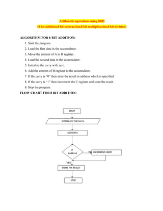
  • 1. Arithmetic operations using 8085 (8 bit addition,8 bit subtraction,8 bit multiplication,8 bit division) ALGORITHM FOR 8-BIT ADDITION: 1. Start the program. 2. Load the first data in the accumulator. 3. Move the content of A to B register. 4. Load the second data in the accumulator. 5. Initialize the carry with zero. 6. Add the content of B register to the accumulator. 7. If the carry is “0” then store the result in address which is specified. 8. If the carry is “1” then increment the C register and store the result. 9. Stop the program FLOW CHART FOR 8 BIT ADDITION:
  • 2. DATA CHECK MAP FOR 8 BIT ADDITION: MEMORY ADDRESS DATA 1 (WITHOUT CARRY) DATA 2 (WITH CARRY) INPUT 8200H 8201H 05 04 FF 03 OUTPUT 8300H(SUM) 8301H(CARRY) 09 00 02 01 PROGRAM FOR 8-BIT ADDITION: MEMORY LABEL MNEMONICS OPCODE COMMENTS 8500 START LDA 8200H 8503 MOV B,A 8504 LDA 8201H 8507 MVI C,00 8509 ADD B 850A JNC LOOP1 850D INR C 850E LOOP1 STA 8300H 8511 MOV A,C 8512 STA 8301H 8515 STOP HLT FLOW CHART FOR 8 BIT SUBTRACTION:
  • 3. ALGORITHM FOR 8 BIT SUBTRACTION: 1. Start the program. 2. Load the first data in the accumulator. 3. Move the content of A to B register. 4. Load the second data in the accumulator. 5. Subtract the content of B register from the accumulator. 6. If the borrow is “0” then go to step 7. 7. Store the result. 8. Stop the program. DATA CHECK MAP FOR 8 BIT SUBTRACTION: MEMORY ADDRESS DATA 1 (WITHOUT BORROW) DATA 2 (WITH BORROW) INPUT 8200H 8201H OUTPUT 8300H 8301H PROGRAM FOR 8 BIT SUBTRACTION:
  • 4. MEMORY LABEL MNEMONICS OPCODE COMMENTS 8500 START LDA 8200H 8503 MOV B,A 8504 LDA 8201H 8507 MVI C,00 8509 SUB B 850A JNC LOOP1 850D INR C 850E LOOP1 STA 8300H 8511 MOV A,C 8512 STA 8301H 8515 STOP HLT FLOW CHART FOR 8 BIT MULTIPLICATION: ALGORITHM FOR 8-BIT MULTIPLICATION:  Start the program.  Load the first data into the accumulator.  Move the content of accumulator to the B register.
  • 5.  Load the second data into the accumulator.  Move the content of accumulator to the C register.  Decrement the content of B register by one.  Add the C register content with accumulator.  Decrement the content of B register & then repeat the steps 7 & 8.  Else store the result in the memory location mentioned.  Stop the program. DATA CHECK MAP FOR 8 BIT MULTIPLICATION: MEMORY LOCATION DATA1 DATA 2 INPUT 8200H 8201H OUTPUT 8300H(Reminder) 8301H(Quotient) PROGRAM FOR 8 BIT MULTIPLICATION: MEMORY LABEL MNEMONICS OPCODE COMMENTS 8500 START LDA 8200H 8503 MOV D,A 8504 LDA 8201H 8507 MOV B,A 8508 DCR D 8509 MVI C,00 850B L2 ADD B 850C JNC 8510 (L1) 850F INR C 8510 L1 DCR D 8511 JNZ 850B (L2) 8514 STA 8300 8517 MOV A,C 8518 STA 8301 851B HLT FLOW CHART FOR 8 BIT DIVISION:
  • 6. ALGORITHM FOR 8 BIT DIVISION:  Start the program.  Load the first data in the accumulator.  Move the content from memory address to A register and increment the HL pair.  Move the content from memory address to B register & initialize the C register.  Compare the 8 bit instructions in A and B registers. Subtract B register from accumulator & increment the value in C register.  Increment the HL pair and move the content in accumulator to memory.  Stop the program.
  • 7. DATA CHECK MAP FOR 8 BIT DIVISION: MEMORY LOCATION DATA1 DATA 2 INPUT 8200H 8201H OUTPUT 8301(Reminder) 8302(Quotient) PROGRAM FOR 8 BIT DIVISION: MEMORY LABEL MNEMONICS OPCODE COMMENTS 8500 START LDA 8200 8503 MOV D,A 8504 LDA 9201 8507 MVI C,00 8509 L1 SUB D 850A INR C 850B CMP D 850C JNC 8509(L1) 850F STA 8300 8512 MOV A,C 8513 STA 9301 8516 HLT PROGRAM WITH 8085-ASCENDING AND DESCENDING ORDER ALGORITHM: (ASCENDING ORDER) 1. Get the numbers to be sorted from the memory locations. 2. Compare the first two numbers and if the first number is larger than second then
  • 8. interchange the number. 3. If the first number is smaller, go to step 4. 4. Repeat steps 2 and 3 until the numbers are in required order. RESULT OF ASCENDING ORDER : MEMORY LOCATION INPUT 8100-15 8101-05 8102-25 8103-10 8104-20 OUTPUT 8100-05 8101-10 8102-15 8103-20 8104-25 PROGRAM: (ASCENDING ORDER) ADD RESS OPCODE LABEL MNEMONICS COMMENTS 8000 MVI B,04 Comparison of N-1 Numbers(5Nos) 8002 LOOP 3 LXI H,8100 8005 MVI C,04 8007 LOOP2 MOV A,M 8008 INX H 8009 CMP M 800A JC LOOP1(8012) 800D MOV D,M 800E MOV M,A 800F DCX H 8010 MOV M,D 8011 INX H 8012 LOOP1 DCR C 8013 JNZ LOOP2(8007)
  • 9. 8016 DCR B 8017 JZ LOOP3(8002) 801A HLT ALGORITHM :( DESCENDING ORDER) 1. Get the numbers to be sorted from the memory locations. 2. Compare the first two numbers and if the first number is SMALLER than second then interchange the number. 3. If the first number is LARGER, go to step 4. 4. Repeat steps 2 and 3 until the numbers are in required order. RESULT OF DESCENDING ORDER : MEMORY LOCATION INPUT 8100-15 8101-05 8102-25 8103-10 8104-20 OUTPUT 8100-25 8101-20 8102-15 8103-10 8104-05 PROGRAM: (DESCENDING ORDER) ADDRESS OPCODE LABEL MNEMONICS COMMENTS 8000 MVI B,04 Comparison of N-1 Numbers(5Nos) 8002 LOOP3 LXI H,8100 8005 MVI C,04 8007 LOOP2 MOV A,M 8008 INX H 8009 CMP M 800A JNC LOOP1(8012) 800D MOV D,M 800E MOV M,A
  • 10. 800F DCX H 8010 MOV M,D 8011 INX H 8012 LOOP1 DCR C 8013 JNZ LOOP2(8007) 8016 DCR B 8017 JZ LOOP3(8002) 801A HLT PROGRAM WITH 8085- MINIMUM AND MAXIMUM NUMBER IN A GROUP OF DATA (Smallest & Largest number ) ALGORITHM :( SEARCH THE MINIMUM NUMBER)
  • 11. 1. Place all the elements of an array in the consecutive memory locations. 2. Fetch the first element from the memory location and load it in the accumulator. 3. Initialize a counter (register) with the total number of elements in an array. 4. Decrement the counter by 1. 5. Increment the memory pointer to point to the next element. 6. Compare the accumulator content with the memory content (next element). 7. If the accumulator content is smaller, then move the memory content (largest element) to the accumulator. Else continue. 8. Decrement the counter by 1. 9. Repeat steps 5 to 8 until the counter reaches zero 10. Store the result (accumulator content) in the specified memory location. RESULT OF SEARCH THE MINIMUM NUMBER: MEMORY LOCATION DATA1 DATA 2 INPUT 8100 8101 8102 8103 8104 25 10 05 30 15 2B 5F 4D 3C 1A OUTPUT 8200 05 1A PROGRAM: (SEARCH THE MINIMUM NUMBER)-SMALLEST NUMBER ADDRESS OPCODE LABEL MNEMONICS COMMENTS 8000 LXI H,8100H 8003 MOV B,05 Comparison of 5 Nos 8005 DEC B 8006 MOV A,M 8007 LOOP1 INX H 8008 CMP M 8009 JC AHEAD(800D) 800C MOV A,M 800D AHEAD DCR B 800E JNZ LOOP1(8007) 8011 STA 8200H 8014 STOP HLT ALGORITHM :( SEARCH THE MAXIMUM NUMBER) 1. Place all the elements of an array in the consecutive memory locations. 2. Fetch the first element from the memory location and load it in the accumulator.
  • 12. 3. Initialize a counter (register) with the total number of elements in an array. 4. Decrement the counter by 1. 5. Increment the memory pointer to point to the next element. 6. Compare the accumulator content with the memory content (next element). 7. If the accumulator content is smaller, then move the memory content (largest element) to the accumulator. Else continue. 8. Decrement the counter by 1. 9. Repeat steps 5 to 8 until the counter reaches zero 10.Store the result (accumulator content) in the specified memory location. RESULT OF SEARCH THE MAXIMUM NUMBER(Largest Number) MEMORY LOCATION DATA1 DATA 2 INPUT 8100 8101 8102 8103 8104 25 10 05 30 15 2B 5F 4D 3C 1A OUTPUT 8200 30 5F PROGRAM: (SEARCH THE MAXIMUM NUMBER)-Largest number ADDRESS OPCODE LABEL MNEMONICS COMMENTS 8000 LXI H,8100H 8003 MOV B,05 Comparison of 5 Nos 8005 DEC B 8006 MOV A,M 8007 LOOP1 INX H 8008 CMP M 8009 JNC AHEAD(800D) 800C MOV A,M 800D AHEAD DCR B 800E JNZ LOOP1(8007) 8011 STA 8200H 8014 STOP HLT STUDY OF ROTATE INSTRUCTION
  • 13. AIM: To rotate and execute an assembly language program to perform instruction. APPARATUS REQUIRED: 1. 8085 kit 2. Power chord ALGORITHM: Program using RLC: 1. Start the program 2. Load the input and add them 3. Then the input values are rotated using RLC 4. Stop the program Program using RRC: 1. Start the program 2. Load the input and add them 3. Now the input is rotated using RRC 4. Stop the program Program using RAL: 1. Start the program 2. Load the input and add them 3. Then the input is rotated using rotate accumulator left through carry 4. Stop the program Program using RAR: 1. Start the program 2. Load the input data and add them 3. Then the input is rotated using rotate the accumulator right through carry 4. Stop the program
  • 14. PROGRAM USING RLC: Memory address Mnemonics Opcode Comments 8100 LXI H,8500 8103 MOV A,B 8104 INX H 8105 ADD M 8106 RLC 8107 STA 8600 810A HLT Program using RRC: Memory address Mnemonics Opcode Comments 8100 LXI H,8500 8103 MOV A,M 8104 INX H 8105 ADD M 8106 RRC 8107 STA 8600 810A HLT Program using RAL: Memory Address Mnemonics Opcode Comments 8100 LXI H,8500 8103 MOV A,M 8104 INX H 8105 ADD M 8106 RAL 8107 STA 8600 810A HLT PROGRAM USING RAR: Memory Address Mnemonics Opcode Comments 8100 LXI H,8500 8103 MOV A,M 8104 INX H 8105 ADD M 8106 RAR 8107 STA 8600 810A HLT RLC: INPUT OUTPUT
  • 15. Memory address Data Memory address data RRC: INPUT OUTPUT Memory address data Memory address data RAL: INPUT OUTPUT Memory address data Memory address data RAR: INPUT OUTPUT Memory address data Memory address data Hex / ASCII / BCD code conversions
  • 16. i. ASCII to Hexa ii. Hexa to ASCII iii.BCD to Hexa iv. Hexa to BCD A) ASCII to Hexa Decimal Conversion: Memory address Label Mnemonics Opcode Comments 8100 LDA 8200 8103 SUI 30 8105 CPI 0A 8107 JC LOOP 810A SUI 07 810C LOOP STA 8300 810F HLT INPUT OUTPUT Memory address Data Memory address Data 8200 41 8300 0A B) Hexa Decimal TO ASCII Conversion:
  • 17. Memory address Mnemonics Opcode Comments 8100 LDA 8200 8103 MOV B,A 8104 ANI 0F 8107 CALL LOOP 8108 STA 8201 8109 MOV A,B 810C ANI F0 810D RLC 810E RLC 810F RLC 8112 RLC 8113 CALL LOOP 8115 STA 8202 8117 HLT LOOP: CPI 0A JC LOOP2 ADI 07 LOOP2: ADI 30 RET INPUT: 8200-E4(hexa value) OUTPUT:8201-34(ASCII code for 4) 8202-45(ASCII code for E) C) BCD to HEX conversion:
  • 18. Memory address Mnemonics Opcode Comments 8100 LXI H,8200 MOV A,M ADD A MOV B,A ADD A ADD A ADD B INX H ADD M INX H MOV M,A HLT INPUT: 8200-02(MSD) 8201-09(LSD) OUTPUT:8202-1DH D) HEXA TO BCD CONVERSION: Memory address LABEL Mnemonics Opcode Comments
  • 19. 8100 LXI H,8200 MOV D,00 XRA A MOV C,M LOOP 2: ADI 01 DAA JNC LOOP1 INR D LOOP1: DCR C JNZ LOOP2 STA 8300 MOV A,D STA 8301 HLT INPUT: 8200-FF OUTPUT: 8300-55(LSB) 8301-02(MSB) 8 CHANNEL ADC INTERFACE with 8085 PROCEDURE: 1. Connect the 26pin FRC to kit and insert power cable. 2. Switch ON the trainer kit. 3. Check all 8 channel input’s and measure it. 4. Enter the given ADC program into the MP/MC kit. 5. If the channel selection is pb2 to pb0 [0 0 0] the CH0 will connect to the MUX output line. Now we get to CH0 corresponding digital value see in LCD. Similarly CH0 to
  • 20. CH7are connected to the MUX output line based on the status of the channel selection for pb2to pb0. 6. Execute the program. 7. Now check stepno.3 8. Repeat the steps 3 and 5. Observe the multiplexer output and ADC output TRUTH TABLE CHANNEL SELECTION: INPUT CHANNEL SELECTION HEX VALUEPB2 PB1 PB0 0 0 0 CHANNEL 0 00 0 0 1 CHANNEL 1 01 0 1 0 CHANNEL 2 02 0 1 1 CHANNEL 3 03 1 0 0 CHANNEL 4 04 1 0 1 CHANNEL 5 05 1 1 0 CHANNEL 6 06 1 1 1 CHANNEL 7 07 ADC CALCULATION: Calculate 1count value. V.REF*2/digital count = 1count 2.5v*2/256 = .0195313v = 19mv Calculate voltage vs digital count. [E:g] 2500mv/19mv = 131.57895 Decimal value Hexadecimal value 131.57895 83 PROGRAM: 8500 3E 90 MVI A, 90 ; CONTROL WORD FOR PORT A AS I/P ; PORT B AND PORT C AS O/P
  • 21. 8502 D3 23 OUT 23 ; OUT IT IN CONTROL REG 8504 3E 40 MVI A, 04 ; CHANNEL SELECTION DATA 8506 D3 21 OUT 21 ; PORT B 8508 3E FF MVI A, FF 850A D3 22 OUT 22 ; PORT C IS ENABLED FOR O/P 850C 3E 00 MVI A, 00 ; START OF CONVERSION 850E D3 22 OUT 22 8510 3E FF MVI A, FF 8512 D3 22 OUT 22 8514 CD 1A 85 CALL 851A ; DELAY ROUTINE 8517 DB 20 IN 20 ; END OF CONVERSION PORTA AS I/P 8519 CF RST 1 ; BREAK POINT 851A 06 0F MVI B, 0F ; DELAY COUNT 851C 3E FF MVI A, FF 851E 00 NOP 851F 00 NOP 8520 3D DCR A 8521 C2 1E 85 JNZ 851E 8524 05 DCR B 8525 C2 1C 85 JNZ 851C 8528 C9 RET ; RETURN TO MAIN PROGRAM CIRCUIT DIAGRAM: ADC INTERFACE
  • 22. INTERFACING 8279 WITH 8085 MICROPROCESSOR (KEYBOARD AND DISPLAY INTERFACE) KEYBOARD PROGRAME FOR 8085: 9000 3E 12 MVI A, 12
  • 23. 9002 32 01 60 STA 6001 9005 3E 3E MVI A, 3E 9007 32 01 60 STA 6001 900A 3E A0 MVI A, A0 900C 32 01 61 STA 6001 900F 06 08 MVI B, 08 9011 3E 00 loop: MVI A, 00 9013 32 00 60 STA 6000 9016 05 DCR B 9017 C2 11 90 JNZ loop 901A 3A 01 60 L1:LDA 6001 901D E6 07 ANI 07 901F CA 1A 90 JZ L1 9022 3A 00 60 LDA 6000 9025 E6 3F ANI 3F 9027 CF RST 1 DISPLAY PROGRAME FOR 8085: 8500 3E 12 MVI A,12 ; control word to define 8279 ; In 8 bit 8 character display 8502 32 01 61 STA 6001 ; 8279 control port 8505 3E 3E MVI A,3E ; for frequency division into 8279 8507 32 01 60 STA 6001 ; into 8279 control reg. 850A 3E A0 MVI A,A0 ; display/write inhibit 850C 32 01 60 STA 6001 ; into 8279 850F 06 08 MVI B,08 8511 3E 00 MVI A,00 ;clear the display 8513 32 00 60 L1: STA 6000 8516 05 DCR B
  • 24. 8517 C2 13 85 JNZ L1 851A 0E 06 MVI C,06 851C 21 00 90 LXI H,9000 ;Input code starting address 851F 7E L2: MOV A,M 8520 32 00 60 STA 6000 8523 23 INX H 8524 0D DCR C 8525 C2 1F 85 JNZ L2 8523 CF RST 1 INPUT CODE ADDRESS: 1ST Digit  9000 2ND Digit  9001 3RD Digit  9002 4TH Digit  9003 5TH Digit  9004 6TH Digit  9005 PORT DETAILS FOR 8086: DATA REGISTER  FF50 STATUS REGISTER  FF52 16 Keys are arranged in 4 X 4 matrix. Their scan codes are as follows: Row 4 - top row of keys (column 1 to 4)  24 23 22 21 Row 3 - (column 1 to 4)  1C 1B 1A 19 Row 2 - (column 1 to 4)  14 13 12 11 Row 1 - bottom row of keys (column 1 to 4)  0C 0B 0A 09 a f b g
  • 25. e c h d D7 D6 D5 D4 D3 D2 D1 D0 D C b a e f g h
  • 26. INTERFACING 8253/8254(TIMER/COUNTER) WITH 8085 Working Description: Enter the program in to the trainer kit. Then give the clock input to the selected Counter. Now run the program and view the output of the selected counter. The user can give his input to the CLK0 or CLK1 or CLK2 from the PCLK through a wire connector. They can view the output pulses in out 0, out 1, out 2 pins. The I/O address for 8085: Counter 0 - 4000 Counter 1 - 4001 Counter 2 - 4002 Control reg - 4003 Steps: Enter the program into the kit. Connect the PCLK and CLK2 through a wire connecter. Now execute the program. Now see the output waveform on the OUT2.
  • 28. PROGRAM FOR 8085 PROGRAM 1: 9000: 3E 37 MVI A, 37 ; cntrl word for 8253.counter 0 is selected 9002: 32 03 40 STA 4003 ; cntrl reg 9005: 3E F7 MVI A, F7 ; LSB of the frequency divider 9007: 32 00 40 STA 4000 ; out it in counter 0 900A: 3E 00 MVI A, 00 ; MSB of the frequency divide 900C: 32 00 40 STA 4000 ; out it in counter 0 900F: CF RST 1 ; end Note: A change in the value of MSB and LSB causes the change in frequency of Counter 0 PROGRAM 2: 9000: 3E 77 MVI A, 77 ; cntrl word for 8253.counter 1 is selected 9002: 32 03 40 STA 4003 ; cntrl reg 9005: 3E F7 MVI A, F7 ; LSB of the frequency divider 9007: 32 01 40 STA 4001 ; out it in counter 1 900A: 3E 00 MVI A, 00 ; MSB of the frequency divider 900C: 32 01 40 STA 4001 ; out it in counter 1 900F: CF RST 1 ; end Note: A change in the value of MSB and LSB causes the change in frequency of Counter 1 PROGRAM 3: 9000: 3E B7 MVI A, B7 ; cntrl word for 8253.counter 2 is selected 9002: 32 03 40 STA 4003 ; cntrl reg 9005: 3E F7 MVI A, F7 ; LSB of the frequency divider 9007: 32 02 40 STA 4002 ; out it in counter 2 900A: 3E 00 MVI A, 00 ; MSB of the frequency divider 900C: 32 02 40 STA 4002 ; out it in counter 2 900F: CF RST 1 ; end
  • 29. Note: A change in the value of MSB and LSB causes the change in frequency of Counter 2 Time Period Amplitude Counter 0 Counter 1 Counter 2
  • 30. DAC INTERFACE Aim: PORT DETAILS FOR 8085: 8255 control register address - 23H 8255 Port A address - 20H 8255 Port B address - 21H 8255 Port C address - 22H DAC PROGRAM FOR 8085: User can give the 8-bit digital data IP at 8501, user can view the output at DAC OP, which is from 2nd pin of DAC (0800), Measure the output voltage using digital Multimeter. 8500 3E80 MVI A, 80h ; CNTRL WORD 8502 D3 23 OUT 23 ; CONTROL REG 8504 3E 00 MVI A,00h ; DIGITAL INPUT DATA1 8506 D3 20 OUT 20h 8508 3E 80 MVI A, 80h ; DIGITAL INPUT DATA 2 850A D3 21 OUT 21 850C 3E 00 MVI A, 00h ; DAC SELECTION DATA (00 OR 01) 850E D3 22 OUT 22 8510 CF RST 1 CALCULATION: 1 count (decimal) = VCC / 256 = 5/ 256 = 0.0196v
  • 31. Output: Digital input output voltage 00 0.0 19 0.5 33 1.0 4C 1.5 66 2.0 7f 2.5 99 3.0 B2 3.5 CC 4.0 E5 4.5 FF 5.0 WORKING PROCEDURE FOR DAC :  Connect the 9 pin D type connector from the DAC module to the Mp/Mc kit.  Connect the 26-pin connector from the DUAL CHANNEL DAC module to Mp/Mc kit.  Connect the keyboard to the Mp/Mc kit.  Switch on the power supply.  Assemble your program.  Execute it and measure the output voltage at the front panel of the DAC module.  Vary the digital count, execute the program and measure the output analog voltage.  Take number of readings and if required draws the graph, DAC input count Vs output voltage to check the linearity.  Switch off the power supply and remove all the connections.
  • 32. 8251 INTERFACE USART PROGRAM FOR 8085: TRANSMIT PROGRAM: 8500 06 55 MVI B, 55 ; Byte to Be TX in B1 Reg 'U' 8502 CD 1D 85 CALL 851D ; Init the counter1to generate 2400 Baud Rate 8505 TXLOOP: 8505 78 MOV A, B ; B - contain the byte to be TX. 8506 CD 0C 85 CALL 850C ; TX one byte to PC 8509 C3 05 85 JMP 8505 850C TXBYTE: 850C CD 4D 85 CALL 854D 850F 47 MOV B, A ; save the byte 8510 LOOOP: 8510 3A 01 60 LDA 6001 ; get the status byte 8513 E6 01 ANI 01 ; check the ready bit 8515 CA 10 85 JZ 8510 8518 78 MOV A, B ; restore the byte to a mode reg 8519 32 00 60 STA 6000 ; TX the byte 851C C9 RET 851D BAUDINIT: 851D 3E 77 MVI A, 77 ; counter1 is selected 851F D3 13 OUT 13 ; out DX, AL 8521 3E 78 MVI A, 78 ; count LSB 8523 D3 11 OUT 11 ; counter1 Reg 8525 3E 00 MVI A, 00 8527 D3 11 OUT 11 ; count MSB 8529 00 NOP 852A 00 NOP
  • 33. 852B 3E 00 MVI A, 00 ; Dummy word 852D 32 01 60 STA 6001 ; Status Register 8530 32 01 60 STA 6001 8533 32 01 60 STA 6001 8536 3E 40 MVI A, 40 ; Reset word 8538 32 01 60 STA 6001 853B CD 4D 85 CALL 854D 853E 3E 4E MVI A, 4E ; 01 00 11 10 8540 32 01 60 STA 6001 ;onestop bit,noparity, 8bits char ; TXC/16 baud 8543 00 NOP 8544 00 NOP 8545 3E 27 MVI A, 27 ; enable TX 8547 32 01 60 STA 6001 854A 00 NOP 854B 00 NOP 854C C9 RET 854D DELAY: 854D 1E 04 MVI E, 04 854F D4: 854F 16 FF MVI D, FF 8551 D3: 8551 00 NOP 8552 00 NOP 8553 00 NOP 8554 00 NOP 8555 00 NOP 8556 00 NOP 8557 00 NOP 8558 15 DCR D 8559 C2 51 85 JNZ 8551 855C 1D DCR E
  • 34. 855D C2 4F 85 JNZ 854F 8560 C9 RET RECEIVER PROGRAM: 8500 CD 13 85 CALL 8513 ;initthecounter1togenerate2400Baud Rate 8503 CD 07 85 CALL 8507 8506 CF RST 1 8507 RXBYTE: 8507 WWW: 8507 3A 01 60 LDA 6001 ;check with the receive over flag 850A E6 02 ANI 02 850C CA 07 85 JZ 8507 850F 3A 00 60 LDA 6000 ; Get the Received Byte 8512 C9 RET 8513 BAUDINIT: 8513 3E 77 MVI A, 77 ; counter1 is selected 8515 D3 13 OUT 13 ; out DX, AL 8517 3E 78 MVI A, 78 ; count LSB 8519 D3 11 OUT 11 ; counter1 reg 851B 3E 00 MVI A, 00 851D D3 11 OUT 11 ; count MSB 851F 00 NOP 8520 00 NOP 8521 3E 00 MVI A, 00 ; Dummy word 8523 32 01 60 STA 6001 ; Status register 8526 32 01 60 STA 6001 8529 32 01 60 STA 6001 852C 3E 40 MVI A, 40 ; Reset word 852E 32 01 60 STA 6001 8531 CD 43 85 CALL 8543 8534 3E 4E MVI A, 4E 8536 32 01 60 STA 6001 8539 00 NOP 853A 00 NOP
  • 35. 853B 3E 27 MVI A, 27 ; enable TX 853D 32 01 60 STA 6001 8540 00 NOP 8541 00 NOP 8542 C9 RET 8543 DELAY: 8543 1E 04 MVI E, 04 8545 D4: 8545 16 FF MVI D, FF 8547 D3: 8547 00 NOP 8548 00 NOP 8549 00 NOP 854A 00 NOP 854B 00 NOP 854C 00 NOP 854D 00 NOP 854E 15 DCR D 854F C2 47 85 JNZ 8547 8552 1D DCR E 8553 C2 45 85 JNZ 8545 8556 C9 RET
  • 36. TRAFFIC LIGHT CONTROLLER Program: PPI: equ 20h ;top 8255 address (in vik-85L kit) ORG 9000H MVI A,80H ;ALL PORTS AS O/P OUT PPI+3 ;----------------------------------------------------------------- ;FOR STARTING VEHICLES N-S DIRECTION(STARIGHT)&PEDESTRIAN STOPPING ;----------------------------------------------------------------- CONTINUE: MVI A,0FH ;FOR PEDESTRIAN OUT PPI+1 ;SIGNAL MVI A,4DH ;FOR GREEN LEDS IN N-S OUT PPI ;DIRECTION CALL DELAY ;SEQUENCE DELAY CALL AMBER ;AMBER DELAY ;----------------------------------------------------------------- ;FOR STOPING VEHICLES IN N-S DIRECTION & STARTING IN E-W DIRECTION ;----------------------------------------------------------------- ;FOR STOPPING N-S SIDES& MVI A,8BH ;STARTING E-W SIDES OUT PPI CALL DELAY ;SEQUENCE DELAY CALL AMBER ;AMBER DELAY ;-----------------------------------------------------------------
  • 37. ;FOR STARIGHT RIGHT TURN IN N-S SIDES& STOPING E-W SIDES ;----------------------------------------------------------------- MVI A,4DH ;FOR FREE LEFT IN ALL SIDES OUT PPI ;& STOPPING IN E-W SIDES ;FOR RIGHT TURN IN N-S SIDES MVI A,0 ;NO RIGHT TURN FROM SOUTH & FROM NORTH OUT PPI+2 CALL DELAY ;SEQUENCE DELAY MVI A,0 ;FOR AMPER OUT PPI+2 ;SIGNAL CALL AMBER ;FOR AMPER DELAY ;----------------------------------------------------------------- ;STOPING RIGHT TURN IN N-S SIDES & STARTING RIGHT TURN IN E-W SIDES ;----------------------------------------------------------------- MVI A,8BH ;FOR STOPPING VEHICLES OUT PPI ;IN N-S SIDES ; ;FOR RIGHT TURN IN MVI A,0 ;E-W SIDES; NO RIGHT FROM EAST AND WEST OUT PPI+2 CALL DELAY ;SEQUENCE DELAY MVI A,0 OUT PPI+2 MVI A,30H OUT PPI MVI B,4 CALL DELAYSUB ;FOR AMBER DELAY ;----------------------------------------------------------------- ;FOR STARTING PEDESTRIAN ;----------------------------------------------------------------- MVI A,0C0H ;FOR STOPPING VEHICLE OUT PPI ;IN ALL SIDES ;GREEN SIGNAL FOR
  • 38. MVI A,0F0H ;PEDESTRIAN OUT PPI+1 MVI B,10H ;DELAY FOR PEDESTRIAN CALL DELAYSUB MVI A,30H OUT PPI MVI B,8 CALL DELAYSUB ;AMBER DELAY JMP CONTINUE AMBER: ;FOR AMBER SIGNAL MVI A,39H ;IN ALL SIDES OUT PPI MVI B,8H ;DEALY COUNT CALL DELAYSUB RET DELAY: MVI B,40H ;DELAY COUNT FOR GREEN& CALL DELAYSUB ;RED SIGNALS RET DELAYSUB: ;DELAY ROUTINE ;R1 * .5SEC BACK2: MVI C,0FFH BACK1:
  • 39. MVI A,0FFH BACK: NOP DCR A JNZ BACK DCR C JNZ BACK1 MOV A,B ORA B JZ OUT DCR B JNZ BACK2 OUT: RET