Introduction to PCB Designing Tutorial
•
2 likes•537 views

Simple steps to learn printed circuit board. PCB Designing tutorial. Learn the tips to understand the concepts of PCB Designing using eagle software.

Recommended
More Related Content
What's hot
What's hot (20)
Similar to Introduction to PCB Designing Tutorial
Similar to Introduction to PCB Designing Tutorial (20)
Recently uploaded
Recently uploaded (20)
Introduction to PCB Designing Tutorial
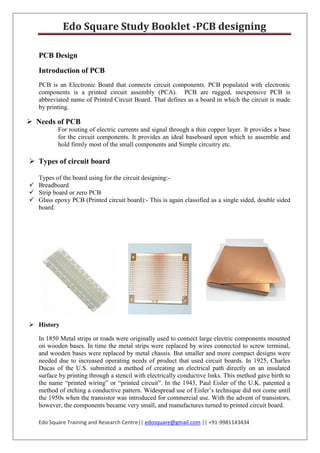
- 1. Edo Square Study Booklet -PCB designing Edo Square Training and Research Centre|| edosquare@gmail.com || +91-9981143434 PCB Design Introduction of PCB PCB is an Electronic Board that connects circuit components. PCB populated with electronic components is a printed circuit assembly (PCA). PCB are rugged, inexpensive PCB is abbreviated name of Printed Circuit Board. That defines as a board in which the circuit is made by printing. Needs of PCB For routing of electric currents and signal through a thin copper layer. It provides a base for the circuit components. It provides an ideal baseboard upon which to assemble and hold firmly most of the small components and Simple circuitry etc. Types of circuit board Types of the board using for the circuit designing:- Breadboard Strip board or zero PCB Glass epoxy PCB (Printed circuit board):- This is again classified as a single sided, double sided board. History In 1850 Metal strips or roads were originally used to connect large electric components mounted on wooden bases. In time the metal strips were replaced by wires connected to screw terminal, and wooden bases were replaced by metal chassis. But smaller and more compact designs were needed due to increased operating needs of product that used circuit boards. In 1925, Charles Ducas of the U.S. submitted a method of creating an electrical path directly on an insulated surface by printing through a stencil with electrically conductive links. This method gave birth to the name “printed wiring” or “printed circuit”. In the 1943, Paul Eisler of the U.K. patented a method of etching a conductive pattern. Widespread use of Eisler’s technique did not come until the 1950s when the transistor was introduced for commercial use. With the advent of transistors, however, the components became very small, and manufactures turned to printed circuit board.
- 2. Edo Square Study Booklet -PCB designing Edo Square Training and Research Centre|| edosquare@gmail.com || +91-9981143434 Steps for PCB design (glass epoxy) 1. Plan – (project – electric circuit – analysis). 2. Layout design (using the EAGLE software). 3. Printing or making layout in paper. 4. Ironing or making layout on PCB. 5. Etching Process. 6. Component Assembly. 7. Soldering. Plan Project plan is termed as an idea that has to be implemented. Firstly make block diagram of idea. Then Choose proper component for plan. Then draw circuit diagram but for circuit diagram knowledge of basic electronic and component is needed. For example:- Let’s plan is to glow led through battery. It needs knowledge of led such that led has one positive terminal and other negative terminal. Now next problem is how to identify terminal of led & how LED work? Let’s connect: Led glow at one’s time and then burn out. For solving these problem read specification of led? Thus This all problem needs knowledge of basic component. Basic Electronics Part Current Electrical current is a measure of the amount of electrical charge transferred per unit time. It represents the flow of charges through a conductive material. The current through the conductor is I=q/t q is the amount of charge flowing through the conductor in t sec. SI unit of the current is Ampere (A) .Now, 1 Ampere = 1 Coulomb / sec=1 Cs-1 Thus current through any conductor is said to be 1 ampere, I f 1 C of charge is flowing through the conductor in 1 sec.
- 3. Edo Square Study Booklet -PCB designing Edo Square Training and Research Centre|| edosquare@gmail.com || +91-9981143434 Voltage A voltage is the difference of electric potentials between two points. Voltage or potential difference between two points in an electric circuit is 1V, if 1j (joule) of energy is expended in transferring 1C of charge between those points. Ohm's law (Georg Ohm, 1787-1854) Ohm's law states that if the physical state of the conductor (Temperature and mechanical strain etc.) remains unchanged, then the potential difference across the two ends of the conductor is always directly proportional to current flowing through a conductor. Mathematically, V α I V= RI V=IR R the electric resistance or simply resistance of the conductor is called constant of proportionality. In general, resistance does not depend on the voltage. Kirchhoff's current law (KCL) At any node (junction) in an electrical circuit, the sum of currents flowing into that node is equal to the sum of currents flowing out of that node. I2 + i3 = i1 + i4 n is the total number of branches with currents flowing towards or away from the node. The current entering any junction is equal to the current leaving that junction. Kirchhoff's voltage law (KVL) Algebraic sum of the voltage in any closed loop is equivalent to the sum of the potential drops in that loop. The sum of all the voltages around the loop is equal to zero. v1 + v2 + v3 - v4 = 0
- 4. Edo Square Study Booklet -PCB designing Edo Square Training and Research Centre|| edosquare@gmail.com || +91-9981143434 Similarly to KCL, it can be stated as Electric circuit An electric circuit is a closed path in which charge flow from a voltage or current source. It consists of some circuit element/component. There are basic two type of circuit element. Passive element The element which required external power (current) for generating power is called Passive element. Example: resistor, inductor capacitor and switches. Active element The element which has small amount of power (current) without external source are called Active element. All semiconductor devices and current & voltage sources are active element. Basic Electronic Component Part An electronic component is any basic discrete device or physical entity in an electronic system of used to affect charges or their associated fields. Resistors A resistor is a component that limits the flow of current inside the circuit. Value of resistance depends upon the nature, dimension and physically dimensions of the conductor. How to select Resistor Selection of resistor depends on the following parameter: Value (measured in ohms) Power rating (in watt) Resistance Tolerance (e.g. ±1%,±2%,±5%,±10%,±15% etc.) Maximum operating voltage (in volts) Operating temperature (in ± degree centigrade) Temperature coefficient (in ppm/°c) Body diameter in mm (used in axial type resistors) How to find the value of Resistor There are two way of finding the value of resistor: Through Multimeter. Colour coding on Colour band placed on it. Resistor value measurement through Multimeter
- 5. Edo Square Study Booklet -PCB designing Edo Square Training and Research Centre|| edosquare@gmail.com || +91-9981143434 Value measurement through Colour code Inductor It is an electrical component that uses magnetism in the storage and release of electrical charge through current. It blocks ac and pass dc.it has mainly two types air core and iron core type. It’s unit is Henry (H). inductor or coil is also used inside the Relay and motors. Capacitor A B C D T F 4 color band 𝑹 = 𝑨𝑩 × 𝟏𝟎^𝑫 ± 𝑻 Ω 5 color band 𝑹 = 𝑨𝑩𝑪 × 𝟏𝟎^𝑫 ± 𝑻 Ω 6 color band 𝑹 = 𝑨𝑩𝑪 × 𝟏𝟎^𝑫 ± 𝑻 𝛀 & 𝑭
- 6. Edo Square Study Booklet -PCB designing Edo Square Training and Research Centre|| edosquare@gmail.com || +91-9981143434 A capacitor is a device that can temporarily store an electric charge. The basic unit of capacitor is the Farad (F), but this value is too large for a practical work so microfarad, Nano- farad and Pico farad is used. Basic Parameters of Capacitor Tolerance. Operating Temperature. Dimensions. Leakage current. Operating voltage. Relay A Relay is a switch that is designed to control other device. Relays can switch high voltages. Relays are a better choice for switching large currents (> 5A). Relays can switch AC and DC. Relays can switch many contacts at once. Basic automatic relay circuit is used a transistor for performing the switching operation. Diode A diode is an electronic component which allows the current to flow through it in one direction but not the other side. A diode can be used as a rectifier which converts AC voltage to DC voltage in power supply applications. Mostly we use 1N4001 to 1N4007 as a freewheeling diode. LED (Light Emitting Diode) It is a device that produces light. There is different colour LED's depending on the semi conducting material. LED has two leads- cathode and anode. The main specification of LED are its current rating=20mA, typical cut in voltage=2V, life time = 2*10^6 hours, approx voltage is around 4.5V. In order to identify the terminal (+ve ,-ve) of the LED see the figure below:
- 7. Edo Square Study Booklet -PCB designing Edo Square Training and Research Centre|| edosquare@gmail.com || +91-9981143434 Transistor A transistor is an electronic component used in a circuit to control a large amount of current or voltage with a small amount of voltage or current. Transistor has three terminal emitter, collector and base. Its leg can be identified through Multimeter or through referring data sheet. The transistor is being used to amplify voltage. Transistors can switch many times per second. Types of transistor: NPN (BC 547, BC548 , BC 549 etc. ) PNP (BC 557 , BC 558 , BC 559 etc.) V –I Charateristics of transistor is given below:
- 8. Edo Square Study Booklet -PCB designing Edo Square Training and Research Centre|| edosquare@gmail.com || +91-9981143434 Transformer A transformer is an electrical device that transfers energy between two circuits through electromagnetic induction. A transformer may be used as a safe and efficient voltage converter to change the AC voltage at its input to a higher or lower voltage at its output without changing the frequency. IC (Integrated Circuits) An integrated circuit is a special component that contains an entire electronic circuit, complete with transistors, diodes, and other elements, all photographically etched onto a tiny piece of silicon. Integrated circuits are the building blocks of modern electronic devices such as computers and cell phones. Voltage regulator(78**) The 7800 series of three-terminal positive regulators is available in TO-220 TO-220FP TO-3 and D2PAK packages and several fixed output voltages, making it useful in a wide range of applications. Each type employs internal current limiting, thermal shut-down and safe area protection, making it essentially indestructible. Although designed primarily as fixed voltage regulators, these devices can be used with external components to obtain adjustable voltages and currents.
- 9. Edo Square Study Booklet -PCB designing Edo Square Training and Research Centre|| edosquare@gmail.com || +91-9981143434 555 Timers Timer IC’s designed for accurate time delays or oscillations. It can be used such as Multi Vibrator and astable Multi Vibrator, and mono stable Multi Vibrator. Comparator IC A comparator is an analog circuit with two inputs and one output. It watches and compares two voltages at the inputs and decides if the output should change or not based on the inputs. Comparators are good at "conditioning" analog signals and turning them into digital signals. There are so many comparator series are available such as LM 358, LM 324 etc. But LM 324 is described here. LM 324 is a quad operational amplifier (op-amp). There are four general purposes Op-amp in the LM324. Each of them can be used as a comparator. Conditioning analog signals and turning them into digital signals. Sensors A sensor is a device that produces a measurable response to a change in a physical condition. Basically sensors are of two types’ Analog sensor and Digital sensor. Some sensors are described below: Light dependent resistor (LDR)
- 10. Edo Square Study Booklet -PCB designing Edo Square Training and Research Centre|| edosquare@gmail.com || +91-9981143434 LDR is basically a resistor whose resistance varies with intensity of light. More intensity less its resistance (i.e. in black it offers high resistance and in white it offers less resistance). Temperature sensor There are many type of temperature sensor available in the market & used. LM 35 is mostly used as a temperature sensor whose output voltage is linearly proportional to the Celsius temperature. The LM35 does not require any external calibration or trimming to provide typical accuracies of ±1⁄4°C at room temperature and ±3⁄4°C over a full −55 to +150°C temperature range. IR sensor It senses the object. It consists of an IR led and Photodiode. It gives both analog and digital output. IR led behaves as transmitter and photodiode behaves as receiver.
- 11. Edo Square Study Booklet -PCB designing Edo Square Training and Research Centre|| edosquare@gmail.com || +91-9981143434 There are ever number of sensors present and use as per requirements like pressure sensor, tilt sensor, ultrasonic sensor, TSOP sensor, jerk sensor, biomedical sensors etc… After getting knowledge of basic electronics & basic circuit component we learn & perform the next steps for PCB designing. Schematic and layout design process Schematic and layout is made either manually or with the help of software. There are so many software are available to use as circuit simulator & layout designing some are: Auto TRAX, Design Spark PCB, DipTrace, EAGLE, Edwinxp, gEDA, KiCad, NI Multisim, PcbExpress, Tina Pro, Free pcb, etc. Easily Applicable Graphical Layout Editor (EAGLE) EAGLE is a powerful graphics editor for designing PC board layouts and schematics. In order to run EAGLE the following is required: Windows 2000, XP, or Vista, Linux based on kernel 2.x for Intel computers, libc6 and X11with a minimum colour depth of 8 bpp, Mac OS X version 10.4 or above (for Power PC or Intel computer), a hard disk with a minimum of 70MByte free disc space, a minimum graphics resolution of 1024 x 768 pixels, preferably a 3buttonmouse.Eagle is made by CadSoft. It has a three edition: Professional edition, Standard edition and light edition. Steps for drawing Schematics Select File/New/Schematic from the Control Panel. Command toolbar which will be displayed in schematic editor window
- 12. Edo Square Study Booklet -PCB designing Edo Square Training and Research Centre|| edosquare@gmail.com || +91-9981143434 Load library frames with use and place a frame of your choice with ADD command.. Using the wire command, draw connection between components. Using the NET command, connect up the pins of the various elements on the drawing. Intersecting nets may be made into connections with the JUNCTION command. Electrical Rule Check (ERC) the ERC command ( ) is used to test schematics for electrical errors. The results are warnings and error messages listed in the ERC window. Using Name command, give name to the component. Using VALUE command, define the value of components. Using INVOKE command; find the hidden terminal of ICs. Using TEXT command describes the circuit and circuit blocks. Using SHOW command check the connection between two terminals. Other different command is used as per requirements. Steps for drawing Layout Design This is the actual design which will be printed on the board. It contains tracks, vias and pads. Click on the toolbar crammed SWITCH TO BOARD for to start laying out the PCB, you should open the schematic and click on the board-button. Placing of Components Use “MOVE” command to drag the various components to the desired positions. The ROUTE command allows the air wires to be converted into tracks. A click on the middle mouse button while a track is being laid allows a change of layer. Clicking with the right mouse button changes the bend of the track. Top layer track Bottom layer track via connecting tracks in different layers Air wire Track bend. Group commend is used to select a group of components & perform other commend for that group.
- 13. Edo Square Study Booklet -PCB designing Edo Square Training and Research Centre|| edosquare@gmail.com || +91-9981143434 Command toolbar in layout editor window RIPUP command is used to convert routed tracks into unrouted signals (air wires). Then use ROUTE command to place track manually. Use DRC command to open design rules setting window and check errors in layout. Use DISPLAY command to set vias, top, bottom pads and different layers in board file. INFO command is used to tack information of component & IC’s and also changes the angle, mirror and position of the component. Text command is used to write something on the PCB. In layout editor window other different command is used as per requirements. Printing Process The PCB layout is a mirrored positive one - black on white. The PCB layout is printed 1:1 on glassy paper by means of a laser printer or copier machine. The laser printer or copier toner will not run out when it gets wet or oily. The generally printer driver properties allow to set the toner density. Always keep maximum toner density. Use a laser printer to print the image on the glassy side of photo paper. Importing (Ironing) Process Firstly clean the copper board with sandpaper. Place layout with toner side on copper of the PCB and then iron it until layout is printed on PCB. Dry the board thoroughly. Make sure that board is
- 14. Edo Square Study Booklet -PCB designing Edo Square Training and Research Centre|| edosquare@gmail.com || +91-9981143434 clean and free from fingerprints place the glassy paper face down on the copper clad board. Use masking tape to hold the paper in position. Place the board on a flat surface. Use very hot iron, to transfer the track pattern from paper to copper board. Don’t be afraid to use lots of heat and pressure. After some time remove the paper from the copper board. If path is broken at some place then need to touch up any broken tracks with an etch resist pen. Etching Process Etching is the process of removing unwanted copper from PCB. Summary of the different methods and their main features that will help you decide which method should use: Acid etching method: This method requires extreme safety measure, the availability of many materials such as the etchant and it is somewhat slow. The quality of PCB obtained varies according to the material but generally, it is a good method for simple to intermediate levels of complexity circuits. Circuits involving more close wiring and tiny wires usually use other methods. This process is easy to used, with low cost and low maintenance. Acid etching material is available in powder and liquid form. UV etching method: This method requires more expensive materials that might not be available everywhere. However, the steps are simple; it requires less safety measures and can produce finer and more complicated circuit layouts. Mechanical etching/routing method: This method requires special machines that will mechanically etch away unnecessary copper from the board or route empty separators between wires. It can be expensive if you intend to buy one of those machines and usually leasing them requires the availability of a workshop nearby. However, this method is good if you need to create many copies of the circuit and also can produce fine PCBs. Laser etching method: This is usually used by large production companies, but can be found on some universities. The concept is similar to mechanical etching but LASER beams are used to etch the board. It is usually hard to access such machines, but if your local university is one of the lucky ones having such machine, you can use their facilities if they allow it. Method of making Acid etching solution Mix 500 gm. Ferric Chloride (FeCl3) with water so it makes 1 liter of solution. This is etching solution. Ferric chloride is a common choice for an etchant. However, you can use Ammonium per sulfate crystals or other chemical solutions also. Drilling Process Drilling is process of making a hole to the PCB. For most purposes a 0.5mm drill is used. Drill all holes with this size first those that need to be larger can be easily drilled again with the appropriate larger size. Types of drilling: Hand drill machine. Electric drill machine Drill bit
- 15. Edo Square Study Booklet -PCB designing Edo Square Training and Research Centre|| edosquare@gmail.com || +91-9981143434 It is cutting tools used to create cylindrical holes, almost always of circular cross-sectional. It is made of Tungsten Carbide. Drilling must be high RPM and high feed to be cost effective. Drill bits must also remain sharp so as not to mar or tear the traces. Bits are held in a tool called a drill, which rotates them and provides torque and axial force to create the hole. The selection of the drill bit is depend upon the drill size of the layout of the circuit or size of the pads & vias of the component. Components Placing From the greatest variety of electronic components available, which runs into thousands of different types it, is often a perplexing task to know which is right for a given job. There could be damage such as hairline crack on PCB. If there are, then they can be repaired by soldering a short link of bare copper wire over the affected part. The most popular method of holding all the items is to bring the wires far apart after they have been inserted in the appropriate holes. This will hold the component in position ready for soldering. Some components will be considerably larger .So it is best to start mounting the smallest first and progressing through to the largest. Before starting, be certain that no further drilling is likely to be necessary because access may be impossible later. Next will probably be the resistor, small signal diodes or other similar size components. Some capacitors are also very small but it would be best to fit these afterwards. When fitting each group of components mark off each one on the circuit as it is fitted so that if we have to leave the job we know where to recommence. Although transistors and integrated circuits are small items there are good reasons for leaving the soldering of these until the last step. The main point is that these components are very sensitive to heat and if subjected to prolonged application of the soldering iron, they could be internally damaged. All the components before mounting are rubbed with sand paper so that oxide layer is removed from the tips. Now they are mounted according to the component layout. Soldering This is the operation of joining the components with PCB after this operation the circuit will be ready to use to avoid any damage or fault during this operation following care must be taken: A longer duration contact between soldering iron bit & components lead can exceed the temperature rating of device & cause partial or total damage of the device. Hence before soldering we must carefully read the maximum soldering temperature & soldering time for device. The wattage of soldering iron should be selected as minimum as permissible for that soldering place. To protect the devices by leakage current of iron its bit should be earthed properly. Safety Precautions Following precaution should be followed. Always be careful, you are working with extreme heat Soldering irons melt metal. So keep away from melt. It can melt skin. They get very hot and can start fires never leave a soldering iron unattended.
- 16. Edo Square Study Booklet -PCB designing Edo Square Training and Research Centre|| edosquare@gmail.com || +91-9981143434 Soldering equipment Solder Iron Solder Stand Soldering flux Soldering wire Soldering Process Heat soldering iron. Always use a clean tip Tin tip soldering iron. Apply solder paste on the PCB or soldering place. Apply heat and solder wire on components terminal. Touch soldering iron to one side of pin, touch solder wire to the other side of the pin Allow solder to flow Remove soldering iron briefly and retouch Solder most items at about 325° C/620 ° F Larger items or components with heat sinks will need higher heat because they dissipate heat well Bigger items like triacs, turn the iron up to 400° C/750 ° F For triacs it may help to trim the legs to desired length before soldering . Let’s make power supply circuit on PCB First draw the block diagram of plan Now choose component Transformer: Full wave centre tapped Transformer of 12 volt and 1amp rating Rectifier: It is either made with the diode IN4007 or either rectifier ic can be used. Filter circuit: Electrolytic capacitor of 1000uf and of 25 volt rating can be used. Voltage regulator: either 7805 or 7812 can be used. Now draw circuit diagram. Source Transformer O/pRectifier 7805 Voltage regulator Filtration ckt
- 17. Edo Square Study Booklet -PCB designing Edo Square Training and Research Centre|| edosquare@gmail.com || +91-9981143434 This is a multiple power supply circuit which produce +12V, +5V & -12V. Draw schematic on EAGLE. Next draw Layout through schematic on Eagle. Take print out of PCB on glassy paper. Glossy paper is multilayer paper that is very helpful in PCB designing. Now cut a copper clad PCB of PCB size. Take a sand paper to rub this PCB.ths will remove corrosion from PCB. This will remove corrosion from PCB. Take layout of PCB and stick this with copper side of PCB. Stick this with copper side of PCB through tape. Now start press or iron copper PCB. After some time layout will be printed on PCB (bottom layer). Put this PCB into the solution and shake thoroughly and observe some part of copper is start removing from PCB. Take out PCB from solution and washed it using water then take sand paper and rub on this PCB till copper track show properly. Now drill of the pad size using drill machine. Now paste the solder and components on right place of circuit and do soldering properly. Circuit diagram of IR sensor