SlideShare a Scribd company logo
1 of 297
Download to read offline
Fundamentals of Electrical and Electronics Engineering
(ECE1002)
Presented By:
Dr. Neeraj Kumar Misra
Associate Professor
Department of SENSE,
VIT-AP University
Google Scholar: https://scholar.google.co.in/citations?user=_V5Af5kAAAAJ&hl=en
Research Gate profile: https://www.researchgate.net/profile/Neeraj_Kumar_Misra
ORCHID ID: https://orcid.org/0000-0002-7907-0276
Introduction: Dr. Neeraj Kumar Misra(Emp. ID: 70442)
Associate Professor, SENSE
▪ Full-time Ph.D (Under TEQIP-II, A World Bank funded Fellowship, Gov. of India)
▪ Post Graduate Diploma in Artificial Intelligence and Machine Learning, from, NIT Warangle.
▪ B.Tech and M.Tech first class with distinction.
▪ Three International Patent granted (Validity 2028),
Patent no. 2021105083, 2020103849, 2020102068
▪ 9+ years of Teaching and Industry Experience
▪ Highest impact factor 8.907 paper published.
▪ Two times Young Achiever Awards in the domain of Quantum Computing
▪ The total 14 publications that were published in the SCI.
▪ Total 03 International books (ISBN: 978-3-659-34118-2, ISBN: 978-613-9-91317-6, ISBN: 978-620-2-01508-0)
▪ Google scholar citation 325, i10-15 and h-index-11.
▪ Funded Project completed 18 Lakh.
▪ Professional Member: IEEE, ACM, ISTE, IETE, WRC, InSc, IAENG, IRED.
▪ Editorial Board Member: ACTA Scientific, JCHE, IEAC, JEEE, IJCS
▪ Total no of Student Guided M.Tech: 10, Ph.D: 03
▪ Most cited paper in the year 2019.
Some reputed organizations
Content
➢ Introduction to Electric Current
a. Transient Current
b. Steady Current
➢ Ohm’s Law: Resistance
➢ The internal resistance of the battery
➢ Numerical Based on Circuit theory
Component
Symbols
Electric Current:
Two Types
1. Transient Current (Very Short duration)
2. Steady Current (Slowly Movement): The charges flow in a steady manner
e.g. Torch, Radio
➢ SI Unit- Ampere
Def: If one coulomb of charge cross an area in one second then the current
through that area in one ampere
1 ampere= 1 coulomb / 1 sec
Electric Current:
➢The cause of flow of current through a conductor is potential difference
applied across its ends.
➢Potential difference is created by battery.
➢The charge will flow in conductor if there is potential difference.
Note:
➢ Electromotive force means work done by the battery per unit charge
➢ E and Fe decrease as free electron accumulate on positive terminal.
➢ Fb depends on the chemical composition of the battery.
Internal Resistance of the battery
R- External resistance
r- internal resistance
Ohm’s Law:
➢Ohm’s law given the relationship between electric current and potential
difference.
➢Potential difference is created by battery. The current flowing through a
conductor is directly proportional to the potential difference applied across
it ends provided the temperature and other physical condition remain
unchanged.
Potential difference current
Where R is the resistance of the conductor
Q.1 Determine the current delivered by the battery and the potential
difference across A and B
Q2. In the given circuit internal resistance 0.1Ώ and EMF=2V and current
I=2A, determine the potential difference and draw the circuit.
Q3. When a cell is connected to 1 Ώ resistance the 1A current flows through
the circuit and when 3 Ώ resistance is issued then 0.5A current flow then find
the internal resistance of the cell.
Numerical Question based on Electric Current
A B
Q.1 Determine the current delivered by the battery and the potential difference across A and B
Q2. In the circuit internal resistance 0.1Ώ and EMF=2V and current I=2A, determine
the potential difference and draw the circuit.
Q3. When a cell is connected to 1 Ώ resistance the 1A current flows through the
circuit and when 3 Ώ resistance is issued then 0.5A current flow then find the
internal resistance of the cell.
Q. Determine
a. Current flow in the circuit (n cell)
b. Current if R<<r
c. Current if R>>r
Q. Determine
a. Current flow in the circuit (n cell)
b. Current if R<<r
c. Current if R>>r
Q. Determine the current flow in the circuit and equivalent emf
Q. Determine the equivalent emf in n-cell, neglect internal resistance
Q. Determine the current flow in the circuit and equivalent emf
Q. Determine the equivalent emf in n-cell, neglect internal resistance
Q. Determine the equivalent emf in 3-cell, neglect internal
resistance.
Q. Find out
a. Equivalent EMF in the given circuit
b. If all the EMF are same and internal resistance are equal
then find equivalent EMF
Q. Find out
a. Equivalent EMF in the given circuit
b. If all the EMF are same and internal resistance are equal then find equivalent EMF
Electric Current: The Junction Law or KCL, or Current Law
➢The sum of all the currents entering a junction in a circuit is equal to the
sum of all the currents leaving it
i entering = i leaving
i outcoming = i outgoing
➢ KCL is based on the ‘conservation of charge’
➢In an electric circuit the algebraic sum of the current meeting at any
junction in the circuit is zero.
➢Current toward junction means positive.
➢Current outwords junction means negative
QUIZ
Q1. For the circuit shown below calculate
𝑰𝟏+𝑰𝟐
𝑰𝟑+𝑰𝟒+𝑰𝟓
QUIZ
Q1. For the circuit shown below calculate
𝑰𝟏+𝑰𝟐
𝑰𝟑+𝑰𝟒+𝑰𝟓
Concept of Open circuit and short circuit
R V I
Open circuit
Short circuit
Q. Fill this below table
Nodal Analysis
Q. Find the voltage across at 2ohm resistance using nodal analysis
Mesh Analysis
Q. Find the current I1 and I2 using mesh analysis
Find the current I1 and I2 using mesh analysis
Basic Concept
Basic Concept
Vacant CB and filled VB Eg is very small as compared to
insulator
A large area of CB is overlapp with
VB
In VB electron has not sufficient
energy to come to CB
Si and Ge most common
semiconductor
Eg= 1.21 (for Si)
= 0.78ev (for Ge) at 0K
Large number of free electron exist
which cause high conductivity and
behave like metal
No current flow (No free electron) At 0K electron can not move from
VB to CB (Like a insulator)
Resistivity is very high At room température few electron
has sufficient energy to reach to CB
Electron coming to CB known as
free electron and the vaccanies
created in VB known as hole
Independent and Dependent Source
Independent Source Dependent Source
• The source which does not depend
on any other quantity like voltage
and current
• Denoted by Circle
• The source whose output value
depends upon the voltage and
current at some part of the circuit
• Denoted by diamond
Q. In the given circuit find out the dependent and independent
source
Dependent Source are broadly classified as
1. Current controlled voltage source (CCVS)
2. Voltage controlled voltage source (VCVS)
3. Current controlled current source (CCCS)
4. Votage controlled voltage source (VCCS)
Current Controlled Voltage Source Voltage Controlled Current Source
➢ Value of dependent source is dependent
on Ix
➢ If value of Ix change then value of
dependent source is changes.
➢ R- Transresistance
G- Transconductance
Voltage Controlled Voltage Source
(VCVS)
Current Controlled Current Source
(CCCS)
➢ Similarity in between VCVS and CCCS gives voltage and current source
scaled value.
Q. What will be the equivalent resistance between terminals P and Q of the
ladder network
Ans. Re=6 ohm
Current to Voltage Source Transformation
and
Voltage to Current Source Transformation
Q. Convert the given circuit into voltage source Q. Convert the given circuit into current source
Q. Use source transformation to find the output voltage (𝑣o)
Current division Rule
Voltage division Rule
Star and Delta Network
➢ In a Star network one common node or neutral point.
➢In a Delta network one closed loop and no any neutral point
Star to Delta Conversion
Delta to Star Conversion
Only Change in Numerator
Q1. Convert Star network into delta network
Q2. Convert delta network into star network
Q1. Find the voltage across 35ohm resistance using star delta conversion
Q1. Find the equivalent resistance between A and B using star delta conversation
Kirchof’s voltage law
➢ KVL deals with the conservation of energy around a closed circuit path.
➢ In a closed loop series path the algebric sum of all the voltage around any
closed loop in a circuit is equal to zero. This is because a circuit loop in a
closed conducting path so no energy is lost.
Q. Find the voltage in the given circuit
Q. Find the voltage across 10ohm resistance (Vx) using mesh analysis
Q. Find the current in and the voltage across 2 ohm resistor
Q. Find the voltage across 6ohm resistance
Q. Obtain the equivalent resistance 𝑅ab for the given circuit and find current i.
Q. Obtain the equivalent resistance at the terminals a-b for the given
circuit.
Q. Find the value of V in the circuit which contain CCVS
Apply KVL in the network
Method-1
Method-2
Voltage Divider Rule
Q. Find the magnitude of total current through R1 and R2 if R1=10Ώ,
R2=20 Ώ and V=50V
Based on the current divider rule
Q. Find the current in the 3 kΩ resistor by converting the current source to
a voltage source
Q. Apply KVL in the circuit and find the current in all the branches
Apply KVL in the given network
Q. Find the current delivered by the battery.
Q. Find the voltage VCE and VAG in the given network
Q. Find the equivalent resistance between terminal B and C
Q. Use mesh analysis to determine i1, i2, i3 and i4.
1. Unidirectional Elements:
When an element properties and characteristic are independent of the current
flow direction then the element is called a unidirectional element.
Concept of Unidirectional and Bidirectional Elements
2. Bidirectional Elements:
When an element properties and characteristic depends on the current flow
direction then the element is called a bidirectional element.
Statement:
In any linear bi-directional circuit having more number of active and passive
elements can be replaced by a single equivalent circuit consisting of an
equivalent voltage source in series with equivalent resistance (Rth)
Thevenin's Theorem
Q. In the given network find the current across load resistance (RL=10ohm)
using the Thevenin theorem.
Hint:
1. Remove the load resistance (RL) and find the open circuit voltage (Voc or Vth)
2. Deactivate the independent source and find Rth of the source side looking through the
circuitry load terminal.
3. Reconnect RL across the load terminal.
4. Find the I across load resistance
Ans I = 0.774 Amp
Step 1: Calculation of Vth or Voc
Remove the load resistance (RL) and find the open circuit voltage (Voc or Vth)
Step 2: Calculation of Rth
Deactivate the independent source and find Rth of the source side looking through the circuitry load terminal.
Step 3: Reconnect RL across the load terminal.
Q. Find the current across 2ohm resistance in the given network using Thevenin theorem.
Ans I= 25/3 Amp
Q. Using Thevenin’s theorem calculate the current flowing through the load resistance RL
connected across the terminals A and B as shown below.
Hint:
1. Remove the load resistance (RL) and find the open circuit voltage (Voc or Vth)
2. Deactivate the independent source and find Rth of the source side looking through the circuitry load
terminal.
3. Reconnect RL across the load terminal.
4. Find the I across load resistance
Ans I= 0.193 Amp
Q. Use Thevenin’s theorem to calculate the current flowing through the 5 Ω resistor in the
circuit shown below
Ans I= 0.8 Amp
Maximum Power Transfer Theorem
Statement
▪ It states that maximum power is transferred to the load when the load
resistance equals the Thevenin resistance (RL = RTh)
Q. Find the value of RL for maximum power transfer in the circuit
and also find the maximum value of power.
Superposition Theorem
Statement:
“In a linear network containing more than one independent source and
dependent source, the resultant current/voltage in any element is the
algebraic sum of the current/voltage that would be produced by each
independent sources acting alone all other independent sources being
replaced by their respective internal resistance.”
Q. Determine the current through the 10ohm resistance using the
superposition theorem.
Hint:
1. Two independent sources (10V and 4A source) which means analysing the circuit two
times.
2. First: 10V acting alone and 4A is open circuit.
3. Second: 4A current source acting alone and 10V battery is a short circuit
1. 10V source acting alone
To find Ix (Fig 2)
Apply the current division rule (Fig 3)
2. 4A source acting alone
Current division rule (fig 2)
Current division rule (fig 1)
By superposition theorem
Unit-II
Alternating Current (AC) Direct Current (DC
An alternating current is that current
whose magnitude changes continuously
with time and direction reverses
periodically.
A direct current is that current which
flows with a constant magnitude in the
same direction
Eg. Electricity supply in home is alternating current In mobile or inverter provide the DC current
Average value of AC over one complete cycle
Mean or average value of AC
It is defined as the value of direct current which sends the same charge in a
circuit in the same time as sent by the given alternating current in its half
time period.
AC Circuit Terminology
Average Value
RMS Value
Q. Find the voltage V in the circuit using the superposition theorem
Step-1 Source 5V acting
Step-2 Source 3A acting
Current division rule
Using superposition theorem
Q. Find the current io in the circuit using the superposition theorem.
Step-1 Source 4A acting
Loop-1
Loop-2
Loop-3
Step-2 Source 20V acting
Using superposition theorem
SuperMesh
➢When a current source is present between two meshes then we remove
the branch having the current source and remaining loop is known as
supermesh.
Q. Find the value of current in 1ohm resistance
Q. Find the current through the 10ohm resistance
Q. Find the current in all the branch and current flow in 2ohm
resistance using supermesh analysis
Terminology: RMS value, Average Value, Form Factor
Form factor=
𝑹𝑴𝑺 𝑽𝒂𝒍𝒖𝒆
𝑨𝒗𝒆𝒓𝒂𝒈𝒆 𝑽𝒂𝒍𝒖𝒆
Q. Calculate the following parameters RMS value, Average Value,
Form Factor in the given waveform
Q. For the triangular waveform which is shown in the below figure, determine the RMS
value, Average Value, Form Factor and Peak Factor
Q. For the trapezoidal voltage waveform which is shown in the below figure,
determine the RMS value, Average Value, Form Factor and Peak Factor
J-Operator
➢When dealing with frequency-dependent sinusoidal sources, we
need to use complex numbers along with real numbers
Concept of Impedance and Admitance
1. Pure resistive circuit
Phasor Diagram: 1. I and V are represented as phasor
2. Rotation in anticlockwise direction
AC circuit with capacitor only
AC circuit with Inductance only
Impedance
Live Quiz-1
Q.1 Which of the following is not ac waveform?
a) sinusoidal
b) square
c) constant
d) triangular
Q.2 The expression for capacitive reactance is given by _____________
a) 1/ωC
b) ω L
c) ωC
d) None of the above
Q3. Which one of the following voltages is obtained from a generator?
a. AC voltage
b. DC voltage
c. Both a and b
d. None of the above
Q. Find out these values in RC Circuit Z, VR, Vc, i, i0, tan φ
Q. Find out these values in RL Circuit Z, VR, VL, i, i0, tan φ
Q. Find out these values in LC Circuit Z, VC, VL, i, i0, tan φ
Q. Find out these values in LC Circuit Z, VC, VL, i, i0
Q. Find out these values in LC Circuit Z, VC, VL, i, i0, and plot Z versus ω
Q. Find out these values in series RLC Circuit Vnet, Z, tan φ, i, i0, resonance
condition, plot i0 versus ω
Q. Find out these values in series RLC Circuit Vnet, Z, tan φ, i, i0, resonance
condition, plot i0 versus ω
Q. Find out these values in series RLC Circuit Vnet, Z, tan φ, i, i0, resonance
condition, plot i0 versus ω
Q. Find out these values in series RLC Circuit Vnet, Z, tan φ, i, i0, resonance
condition, plot i0 versus ω
Q. Find out these values in series RLC Circuit Vnet, Z, tan φ, i, i0, resonance
condition, plot i0 versus ω
Q. Find out these values in parallel RLC Circuit Vnet, Z, tan φ, i, i0,
resonance condition, plot i0 versus ω
Concept of Power, Average power, real power, virtual
power and power factor in AC circuit
* Power in AC circuit Pm = Vm x Im (Where Vm and Im represent instantaneous value)
* Average power Pavg= (This is one method to calculate average power, but it is complex)
Instantaneous value of V
Instantaneous value of I
Instantaneous value of P
Concept of Power, Average power, real power, virtual power and power factor in AC circuit
Q1. Find out the impedance of the following circuit
Q2. Find out the Z, I, power factor, Voltage phasor diagram for the given circuit
Live Quiz
Q. Find the node voltages (V1 and V2) of the following circuit.
Concept of Virtual Power and Real Power
➢Virtual power is not real power
➢In virtual power phase difference is not considered.
➢In real power phase difference is considered.
➢In real power phase angle is considered
➢If the phase angle is increased then the power factor increases and
vice versa
Concept of Virtual Power and Real Power
Average Power in Pure Resistive element
Average Power in Inductive and Capacitive element
Average Power in Pure resistive element
Average Power in RLC circuit
Concept of Power Factor
1. Power factor (Pf) is the cosine of the phase difference between voltage and
current.
2. Pf is dimensionless.
➢ Pf is the cosine of the angle of the load impedance.
Concept of Complex Power
➢ Voltage and current must be in phasor form
➢ Complex power (S) absorbed by ac load
Concept of Complex Power
➢ P is the real part of a complex number
➢ Q is the imaginary part of a complex
number
Concept of real power and reactive power
Real Power: Real power is the useful power or average power delivered to a
load. Load dissipate the power is known as real power.
Reactive Power: Reactive power is the power to delivered to source to load and
load to source and it not dissipate by load.
Reactive power value in resistive, capacitive and inductive load
Pure resistive Capacitive Load Inductive Load
Power Triangle, and Impedance Triangle
Power Triangle Impedance Triangle
Q1. If the load impedance angle is 45 degrees find the power factor.
Q2. Find the instantaneous power and the average power absorbed
Q3. Find the average power applied by the source and the average power
absorbed by the resistor
Q1. If the load impedance angle is 45 degrees find the power factor.
Q2. Find the instantaneous power and the average power absorbed
Q3. Find the average power applied by the source and the average power
absorbed by the resistor
Q3. The voltage across a load is 𝒗(𝒕) = 𝟔𝟎𝒄𝒐𝒔(𝝎𝒕 − 𝟏𝟎°)𝑽 and the current
through the element in the direction of the voltage drop is
𝒊(𝒕) =𝟏. 𝟓𝒄𝒐𝒔(𝝎𝒕 + 𝟓𝟎°)𝑨
Find:
(a) The complex and apparent powers,
(b) The real and reactive powers,
(c) The power factor and the load impedance.
Valance Band Conduction Band
The valence band consists of the electrons that
lie in the outermost shell or valence shell of the
atom.
The conduction band consists of the free
electrons that take part in the process of
conduction.
The valence band lies below the Fermi level. The conduction band lies above the Fermi
level.
When external energy is given to the electrons
in the valence they leave the valence band.
When external energy is given to the electrons
they leave the valence band and reach the
conduction band.
There is no flow of current due to the electrons
present in the valence band.
The free electrons present in the conduction
band are free to move anywhere within the
volume of the solid, therefore current flows
due to these electrons.
Due to the presence of electrons valence band
is partially or completely filled.
The conduction band is either empty or
partially filled.
Remember
➢ Hole is a seat of positive charge which is produced when an electron breaks away from a
covalent bond in a semiconductor.
➢ Hole carries a unit positive charge.
➢ Hole has the same charge as that of electron.
➢ Energy of a hole is high as compared to that of electron.
➢ The mobility of hole is smaller
➢ The three acceptor impurities are Aluminium, Indium, and gallium.
➢ The three donor impurities are Phosphorus, Antimony, and Arsenic.
➢ In n-type semiconductor: Both electrons and holes exist as charge carriers in n-type semiconductor.
However, electrons are majority charge carriers while holes are minority charge carriers.
Silicon is preferred to germanium in the manufacture of semiconductor devices due to following
reasons.
➢ The leakage current in silicon is very small as compared to that of germanium.
➢ In case of silicon, the leakage current is less effected with temperature as compared to germanium.
➢ The working temperature of silicon is more than that of germanium. The structure of germanium
gets destroyed at a temperature of about 100 °C but silicon can be operated upto about 200°C.
Donar and Accepter Ions
Intrinsic Semiconductor Extrinsic Semiconductor
Pure forms of semiconductors Extrinsic semiconductors are made by adding some
impurity to the pure form of semiconductors.
They exhibit poor electrical conductivity. Electrical conductivity in the case of extrinsic
semiconductors is significantly high as compared to
intrinsic semiconductors.
Intrinsic semiconductors, the number of free
electrons in the conduction band is equal to the
number of holes in the valence band.
The number of electrons and holes are not equal in
extrinsic semiconductors and depends on the type of
extrinsic semiconductor.
The electrical conductivity of intrinsic
semiconductors depends only on the temperature.
The electrical conductivity of extrinsic
semiconductors depends on the temperature as well
as the amount of doped impurity.
In intrinsic semiconductors, the Fermi energy levels
lie in the middle of the valence and conduction band.
In extrinsic semiconductors, the Fermi level shifts
towards the valence or conduction band.
Examples include the crystalline forms of pure silicon
or germanium.
Examples include Silicon (Si) and germanium (Ge)
crystals with impurity atoms of As, Sb, P, etc., or In,
B, Al, etc.
P-type semiconductor N-type semiconductor
P-type semiconductors are formed due to
doping of elements of group III i.e. Boron,
Aluminium, Thallium, etc.
N-type semiconductors are formed due to
doping of elements of group V i.e. Nitrogen,
Phosphorus, Arsenic, Antimony, Bismuth, etc.
Holes are the majority carriers in P-type
semiconductors.
Electrons are the majority carriers in n-type
semiconductors.
Electrons are the minority carriers in P-type
semiconductors.
Holes are minority carriers in N-type
semiconductors.
The fermi energy levels of these materials lie
between the impurity energy level and the
valence band.
The Fermi levels of these materials lie between
the impurity energy level and the conduction
band.
The movement of majority carriers is from
higher potential to lower potential.
The movement of majority carriers is from
lower potential to higher potential.
In P-type semiconductors, hole density is
greater than the electron density.
Nh > Ne
Electron density is much greater than the hole
density for the n-type semiconductors.
Ne > Nh
n-type Semiconductor
Extrinsic semiconductor: N type semiconductor
Extrinsic semiconductor: P type semiconductor
Extrinsic semiconductor: N and P -type semiconductor
P-N Junction diode
Need to learn this concept
1. P-N Junction diode
2. Depletion region
3. Immobile charge
4. Potential barrier
5. Diffusion current
6. Drift current
7. Forward biased
8. Reverse biased
P-N Junction diode
Depletion Region
➢The region on either of the junction which becomes depleted (free) of
the mobile charge carrier is called the depletion region.
➢Positive and Negative ions fixed in their position are known as the
Depletion region.
Potential Barrier (Vb)
➢The potential difference created across the PN junction due to
diffusion of electron and hole is called potential barrier
➢Vb= 0.3V (Ge), 0.7V (Si)
➢Deflection width is very small: 10-6 m
Due to the high electric field, electrons do not cross the barrier similar
hole also not cross the barrier.
Diffusion Current
➢ Due to the difference in concentration of charge carrier hole and electron start
diffusion from one side to another side. This diffusion result is an electric current
from P-side to N-side is known diffusion current.
Drift Current
➢ Drift current flow due to thermal energy, collision, covalent bond break, electron-hole
pair created. Due to these above effect hole move towards P-side and electron move
towards n-side.
➢ Drift current and diffusion current are in opposite direction
Forward and Reversed Biased
Forward Biased Reversed Biased
In forward biased positive terminal of the battery is connected to the
P-Type and the negative terminal of the battery is connected to N-
Type
In reversed biased positive terminal of battery is connected to N-
Type and negative terminal of battery is connected to P-Type
Forward biased opposes the potential barrier and for V>Vb and
forward current is setup across the junction.
Reverse biased support the potential barrier and no current flow
across the junction due to diffusion of majority carrier.
Width of the depletion region decrease. That means a large current
will flow in the device.
Width of the depletion region increase. That means very small
reverse current may exist (Microampere)
Knee (Voltage): The voltage at which the current start to increase. Breakdown voltage: Reverse voltage in which the breakdown of the
semiconductor occurs.
Forward and Reversed Biased
Forward Biased Reversed Biased
Small current in microampere due to the
motion of the few thermally generated
minority carriers (Electron in p region and
hole in n-region) whose motion is added by
the applied voltage.
Q. Two ideal diode are connected in parallel. What is the current flow
in the circuit?
Q.1 Find VD, VR, and ID in the given circuit.
Q2. Find V0, and ID in the given circuit.
Q3. Find ID, VD2, and V0 in the given circuit.
Q4. Find V0 in the given circuit
Problem Based on Diode
Q5. Find V0 in the given circuit
Problem Based on Diode
Q5. Find V0 in the given circuit
Problem Based on Diode
➢ When a reverse bias is increased the electric field
at the junction also increases. At some stage, the
electric field becomes so high that it breaks the
covalent bonds creating electron, hole pairs.
➢ Thus a large number of carriers are generated.
This causes a large current to flow. This
mechanism is known as Zenor breakdown.
➢ Zener diode is used in reverse biased, and it is
used for voltage regulation.
Zenor breakdown.
➢ At high reverse voltage due to a high electric
field, the minority charge carriers while crossing
the junction acquire very high velocities.
➢ These by collision breaks down the covalent
bonds, generating more carriers. A chain
reaction is established giving rise to high
current. This mechanism is called avalanche
breakdown.
➢ The avalanche breakdown occurs in a lightly
doped junction.
Avalanche breakdown
Difference between Zener and Avalanche Breakdown
Zenor Diode as Voltage Regulation
➢ Voltage across Zenor- Vz
➢ Purpose of Zenor diode
To get a constant dc voltage from the unregulated
input of a rectifier.
➢ The input voltage may vary but the output
regulated
Zenor Diode as Voltage Regulation
Q. The reverse breakdown voltage of a zenor diode is 5.6V in the given circuit. Find
the current IL through the load resistance.
Zenor Diode as Voltage Regulation
Q. Figure shows a DC voltage regulator circuit with a zener diode of breakdown
voltage=6V. If the unregulated input voltage between 10V to 16V then what is the
maximum zener current?
Zenor Diode as Voltage Regulation
Q. A 5.0V stabilized power supply is required to be produced from a 12V DC power
supply input source. The maximum power rating PZ of the Zener diode is 2W.
Using the Zener regulator circuit above calculate:
a) The maximum current flowing through the Zener diode.
b) The minimum value of the series resistor, RS
c) The load current IL if a load resistor of 1kΩ is connected across the Zener diode.
d) The Zener current IZ at full load.
Diode as Rectifier
In half wave rectifier diode conduct in positive half cycle and does not conduct
during the negative half cycle. Hence AC is converted by diode into unidirectional
pulsating DC. This action is known as half wave rectifier.
Diode as the Half Wave Rectifier
In full-wave rectifier two p-n junction diode D1 and D2 are used.
Diode as the Full Wave Rectifier
Bridge Rectifier
➢ During positive cycle D1 and D2 forward bias (Closed Circuit)
➢ During negative cycle D3 and D4 forward bias (Closed Circuit)
Ripple Factor
➢ The ripple factor measures the percentage of ac components in the rectified
output.
➢ The ideal value of ripple factor should be zero.
rms value of ac component of output
Ac value of output
Ripple factor of half wave rectifier=1.21 or 121%
Efficiency of half wave rectifier=40.6%
Q. What should be the value of R such that maximum power
transfer can place in the following circuit? Find the maximum
power transferred from the rest of the network to the R.
Maximum Power Transfer Theorem
Q. Find the voltage across 10ohm resistance (Vx) using mesh analysis
Q. The voltage across a load is 𝒗(𝒕) = 𝟔𝟎𝒄𝒐𝒔(𝝎𝒕 − 𝟏𝟎°)𝑽 and the current through
the element in the direction of the voltage drop is
𝒊(𝒕) =𝟏. 𝟓𝒄𝒐𝒔(𝝎𝒕 + 𝟓𝟎°)𝑨
Find:
(a) The complex and apparent powers,
(b) The real and reactive powers,
(c) The power factor and the load impedance.
Q. Find the current I in the load resistance using nodal analysis
Q. Determine the dc resistance level for the diode
a. ID= 2 mA
b. ID=20mA
c. VD=-10V
Q. For the trapezoidal voltage waveform which is shown in the below
figure, determine the RMS value, Average Value, Form Factor and Peak
Factor
Q. For the triangular waveform which is shown in the below figure, determine the RMS
value, Average Value, Form Factor and Peak Factor
Q. Using Thevenin’s theorem calculate the current flowing through the
load resistance RL connected across the terminals A and B as shown.
Q. Find the current io in the circuit using the superposition theorem.
Step-1 Source 4A acting
Loop-1
Loop-2
Loop-3
Step-2 Source 20V acting
Using superposition theorem
Q. Over what range of input voltage will the zener circuit shown in Figure below
maintain 30 V across 2000 Ω load, assuming that series resistance R = 200 Ω and zener
current rating is 25 mA ?
Q. Over what range of input voltage will the Zener diode maintain 30V across
2000ohm, assuming that series resistance R=200ohm and Zener diode rating is
25mA.
Bipolar Junction Transistor (BJT)
➢ There are three terminals of BJT. These terminals are known as collector (C), emitter (E)
and base (B)
➢ All regions (E, B and C) have different thicknesses and doping levels.
➢ Emitter is used to emit all the charges and Collector is used to collect all the charges.
Terminal Doping Size
Emitter Heavily doped
Supplies/Emit majority charge carrier
Thinner than collector
And
Thicker than base
Base Lightly doped Very thin
Passes charge carriers to collector
Collector Moderate doped Thickest in size
Collect or remove majority charge carrier
coming from emitter
Working of PNP Transistor
Transistor Configuration
A transistor can be connected in the circuit in the following three ways
➢ Common base (CB)
➢ Common emitter (CE)
➢ Common collector (CC)
Common base (CB) configuration:
Input and Output Characteristics of Common base (CB) configuration:
a. Input Characteristics:
Input and Output Characteristics of Common base (CB) configuration:
a. Output Characteristics:
Transistor Biasing:
Note:
In Forward biased: p must be connected to the Positive terminal
n must be connected to the negative terminal
In Reversed biased: n must be connected to the Positive terminal
p must be connected to the negative terminal
forward-reverse bias.
Direction of Current in PNP and NPN Transistor
forward-reverse bias.
Diode representation of Transistor
Transistor Biasing
➢Transistor Biasing is the process of setting a transistor DC operating voltage or current
conditions to the correct level so that any AC input signal can be amplified correctly by the
transistor.
➢Biasing is used to set the Q-point.
➢The process of applying dc voltage across the different junctions of the transistor is called
biasing.
Transistor Biasing
1. Active: Used for amplification
2. Saturation: Ic is independent of base current IB
Transistor work as switch and closed
3. Cut-off: Emittter terminal not emit any charge
and transistor work as open switch
4. Inverted: Emitter is heavily doped and
A collector is moderately doped
This region action is very poor.
Transistor Biasing
Q-Point
➢ When a line drawn over the output characteristic curve, the line makes a
contact at a point this is known as the operating point or Q-point.
Q-Point
Biasing Types
1. Fixed bias
2. Voltage divider bias
3. Collector to base bias
Biasing Types
1. Fixed bias
Biasing Types
1. Fixed bias
Biasing Types
1. Fixed bias
Q. Calculate the emitter current, IE and collector voltage, VC.
Op-Amp (Operational Amplifier)
➢ Op-Amp is an IC to amplify the input voltage with Av (Gain) times and provides a high output voltage.
➢Op-Amp is the voltage-controlled, voltage source device.
➢Gain of Op-Amp varies with a different type of Op-Amp IC.
Symbol of Op-Amp
➢ For high amplification, the gain must be high
➢ For Op-Amp Av (gain) is very high.
Symbol of Op-Amp
➢ Input resistance Ri= (Means it open circuit and no drop on the input side)
➢ Output resistance R0 = 0 (Means gain to be maintained and no drop, then the output voltage is very high.
Properties of Ideal Op-Amp
Open-Loop Gain= for (Ideal Op-Amp)
Op-Amp Types
1. Inverting
2. Non-inverting
3. Differential
1. Inverting: Invert the input signal 2. Non-inverting: The input signal is not inverted
Op-Amp Types
3. Differential
Inverting amplifier with feedback
➢ Negative feedback means output voltage connected to the negative terminal
Non-Inverting amplifier with feedback
Numerical Questions based on inverting and non-inverting amplifier
Q1. Determine the voltage gain of the op-amp for the given circuit
Numerical Questions based on inverting and non-inverting amplifier
Q2. Determine the output voltage of the 3-input adder circuit as shown below
Numerical Questions based on inverting and non-inverting amplifier
Q3. Determine the output voltage of the op-amp for the given circuit
Numerical Questions based on inverting and non-inverting amplifier
Q4. Determine the output voltage of the op-amp for the given circuit
Numerical Questions based on inverting and non-inverting amplifier
Q5. Determine the output voltage of the op-amp for the given circuit
Common Mode Rejection Ratio (CMRR)
Common mode Signal Differential mode signal
Common Mode Rejection Ratio (CMRR)
Differential Mode Common mode input

More Related Content

What's hot (20)

Schottky diode
Schottky diodeSchottky diode
Schottky diode
 
Electrical Engineering
Electrical EngineeringElectrical Engineering
Electrical Engineering
 
Tunnel diode
Tunnel diodeTunnel diode
Tunnel diode
 
Photo diode
Photo diodePhoto diode
Photo diode
 
Field Theory.pptx
Field Theory.pptxField Theory.pptx
Field Theory.pptx
 
Slew rate, Open and closed loop configurations
Slew rate, Open and closed loop configurationsSlew rate, Open and closed loop configurations
Slew rate, Open and closed loop configurations
 
7.instrumentation amplifier
7.instrumentation amplifier7.instrumentation amplifier
7.instrumentation amplifier
 
Mosfet
MosfetMosfet
Mosfet
 
MOSFETs
MOSFETsMOSFETs
MOSFETs
 
Scattering matrix
Scattering matrixScattering matrix
Scattering matrix
 
Pn junction diode by sarmad baloch
Pn junction diode by sarmad balochPn junction diode by sarmad baloch
Pn junction diode by sarmad baloch
 
Presentation on Op-amp by Sourabh kumar
Presentation on Op-amp by Sourabh kumarPresentation on Op-amp by Sourabh kumar
Presentation on Op-amp by Sourabh kumar
 
Bjt oscillators
Bjt oscillatorsBjt oscillators
Bjt oscillators
 
Op-Amp Fundamental
Op-Amp FundamentalOp-Amp Fundamental
Op-Amp Fundamental
 
Field Effect Transistor (FET) and it's Types
Field Effect Transistor (FET) and it's TypesField Effect Transistor (FET) and it's Types
Field Effect Transistor (FET) and it's Types
 
Power amplifire analog electronics
Power amplifire analog electronicsPower amplifire analog electronics
Power amplifire analog electronics
 
Basics of MOSFET
Basics of MOSFETBasics of MOSFET
Basics of MOSFET
 
Moving Coil Microphone
Moving Coil MicrophoneMoving Coil Microphone
Moving Coil Microphone
 
Bjt amplifiers
Bjt amplifiersBjt amplifiers
Bjt amplifiers
 
LED
LEDLED
LED
 

Similar to Fundamental of Electrical and Electronics Engineering.pdf

Basic Circuit Lec 2.pptx
Basic Circuit Lec 2.pptxBasic Circuit Lec 2.pptx
Basic Circuit Lec 2.pptxgetacew1
 
RGPV BE Ist SEM BEE104 Unit I
RGPV BE Ist SEM BEE104 Unit IRGPV BE Ist SEM BEE104 Unit I
RGPV BE Ist SEM BEE104 Unit IMani Deep Dutt
 
Circuit Theory Question Bank
Circuit Theory Question BankCircuit Theory Question Bank
Circuit Theory Question BankSanthosh Kumar
 
Conductors, Capacitors, Dielectrics
Conductors, Capacitors, Dielectrics Conductors, Capacitors, Dielectrics
Conductors, Capacitors, Dielectrics josealberto21
 
B tech ee ii_ eee_ u-1_ dc circuit analysis_dipen patel
B tech ee  ii_ eee_ u-1_ dc circuit analysis_dipen patelB tech ee  ii_ eee_ u-1_ dc circuit analysis_dipen patel
B tech ee ii_ eee_ u-1_ dc circuit analysis_dipen patelRai University
 
Diploma i boee u 2 dc circuit analysis
Diploma i boee u 2 dc circuit analysisDiploma i boee u 2 dc circuit analysis
Diploma i boee u 2 dc circuit analysisRai University
 
Network Analysis Part-1 GATE ESE PSU NTPC BHEL RRB SSC MPEB DMRC RRB technic...
Network Analysis Part-1 GATE ESE PSU NTPC BHEL RRB SSC MPEB DMRC RRB  technic...Network Analysis Part-1 GATE ESE PSU NTPC BHEL RRB SSC MPEB DMRC RRB  technic...
Network Analysis Part-1 GATE ESE PSU NTPC BHEL RRB SSC MPEB DMRC RRB technic...Prasant Kumar
 
Superposition and norton Theorem
Superposition and norton TheoremSuperposition and norton Theorem
Superposition and norton TheoremMahmudul Alam
 
EE110-elementary-circuit-and-network-theory-(a)
EE110-elementary-circuit-and-network-theory-(a)EE110-elementary-circuit-and-network-theory-(a)
EE110-elementary-circuit-and-network-theory-(a)rsamurti
 
BASIC ELECTRICAL ENGINEERING BEEE
BASIC ELECTRICAL ENGINEERING BEEE BASIC ELECTRICAL ENGINEERING BEEE
BASIC ELECTRICAL ENGINEERING BEEE Prasant Kumar
 
Electrical Servuces_MOD I_I.pptx
Electrical Servuces_MOD I_I.pptxElectrical Servuces_MOD I_I.pptx
Electrical Servuces_MOD I_I.pptxssuser3f3a21
 
IGCSE-CL10-CH 18-ELEC QTTIES.pptx
IGCSE-CL10-CH 18-ELEC QTTIES.pptxIGCSE-CL10-CH 18-ELEC QTTIES.pptx
IGCSE-CL10-CH 18-ELEC QTTIES.pptxRachnaRishi2
 
Phy & Elec 04-08.pdf
Phy & Elec 04-08.pdfPhy & Elec 04-08.pdf
Phy & Elec 04-08.pdfFakhr2
 
Electrical and Electronics Engineering
Electrical and Electronics EngineeringElectrical and Electronics Engineering
Electrical and Electronics EngineeringEkeeda
 
Electric current and dc circuits.
Electric current and dc circuits.Electric current and dc circuits.
Electric current and dc circuits.MlokotiSikhulule
 
Electricity.Electronics Ch20
Electricity.Electronics Ch20Electricity.Electronics Ch20
Electricity.Electronics Ch20Nisa Sho
 
Additional Science P2.3 Electricity
Additional Science P2.3 ElectricityAdditional Science P2.3 Electricity
Additional Science P2.3 ElectricitySteve Bishop
 

Similar to Fundamental of Electrical and Electronics Engineering.pdf (20)

Basic Circuit Lec 2.pptx
Basic Circuit Lec 2.pptxBasic Circuit Lec 2.pptx
Basic Circuit Lec 2.pptx
 
RGPV BE Ist SEM BEE104 Unit I
RGPV BE Ist SEM BEE104 Unit IRGPV BE Ist SEM BEE104 Unit I
RGPV BE Ist SEM BEE104 Unit I
 
Circuit Theory Question Bank
Circuit Theory Question BankCircuit Theory Question Bank
Circuit Theory Question Bank
 
Conductors, Capacitors, Dielectrics
Conductors, Capacitors, Dielectrics Conductors, Capacitors, Dielectrics
Conductors, Capacitors, Dielectrics
 
Unit 1.doc
Unit 1.docUnit 1.doc
Unit 1.doc
 
B tech ee ii_ eee_ u-1_ dc circuit analysis_dipen patel
B tech ee  ii_ eee_ u-1_ dc circuit analysis_dipen patelB tech ee  ii_ eee_ u-1_ dc circuit analysis_dipen patel
B tech ee ii_ eee_ u-1_ dc circuit analysis_dipen patel
 
Diploma i boee u 2 dc circuit analysis
Diploma i boee u 2 dc circuit analysisDiploma i boee u 2 dc circuit analysis
Diploma i boee u 2 dc circuit analysis
 
Network Analysis Part-1 GATE ESE PSU NTPC BHEL RRB SSC MPEB DMRC RRB technic...
Network Analysis Part-1 GATE ESE PSU NTPC BHEL RRB SSC MPEB DMRC RRB  technic...Network Analysis Part-1 GATE ESE PSU NTPC BHEL RRB SSC MPEB DMRC RRB  technic...
Network Analysis Part-1 GATE ESE PSU NTPC BHEL RRB SSC MPEB DMRC RRB technic...
 
Electric current and_ohms_law1
Electric current and_ohms_law1Electric current and_ohms_law1
Electric current and_ohms_law1
 
Superposition and norton Theorem
Superposition and norton TheoremSuperposition and norton Theorem
Superposition and norton Theorem
 
EE110-elementary-circuit-and-network-theory-(a)
EE110-elementary-circuit-and-network-theory-(a)EE110-elementary-circuit-and-network-theory-(a)
EE110-elementary-circuit-and-network-theory-(a)
 
BASIC ELECTRICAL ENGINEERING BEEE
BASIC ELECTRICAL ENGINEERING BEEE BASIC ELECTRICAL ENGINEERING BEEE
BASIC ELECTRICAL ENGINEERING BEEE
 
Electrical Servuces_MOD I_I.pptx
Electrical Servuces_MOD I_I.pptxElectrical Servuces_MOD I_I.pptx
Electrical Servuces_MOD I_I.pptx
 
IGCSE-CL10-CH 18-ELEC QTTIES.pptx
IGCSE-CL10-CH 18-ELEC QTTIES.pptxIGCSE-CL10-CH 18-ELEC QTTIES.pptx
IGCSE-CL10-CH 18-ELEC QTTIES.pptx
 
Phy & Elec 04-08.pdf
Phy & Elec 04-08.pdfPhy & Elec 04-08.pdf
Phy & Elec 04-08.pdf
 
Electrical and Electronics Engineering
Electrical and Electronics EngineeringElectrical and Electronics Engineering
Electrical and Electronics Engineering
 
Electric current and dc circuits.
Electric current and dc circuits.Electric current and dc circuits.
Electric current and dc circuits.
 
Electricity.Electronics Ch20
Electricity.Electronics Ch20Electricity.Electronics Ch20
Electricity.Electronics Ch20
 
ELECTRICITY.ppt-converted.pptx
ELECTRICITY.ppt-converted.pptxELECTRICITY.ppt-converted.pptx
ELECTRICITY.ppt-converted.pptx
 
Additional Science P2.3 Electricity
Additional Science P2.3 ElectricityAdditional Science P2.3 Electricity
Additional Science P2.3 Electricity
 

More from VIT-AP University

Cost-effective architecture of decoder circuits and futuristic scope in the e...
Cost-effective architecture of decoder circuits and futuristic scope in the e...Cost-effective architecture of decoder circuits and futuristic scope in the e...
Cost-effective architecture of decoder circuits and futuristic scope in the e...VIT-AP University
 
Information Theory and Coding
Information Theory and CodingInformation Theory and Coding
Information Theory and CodingVIT-AP University
 
Efficient architecture for arithmetic designs using perpendicular NanoMagneti...
Efficient architecture for arithmetic designs using perpendicular NanoMagneti...Efficient architecture for arithmetic designs using perpendicular NanoMagneti...
Efficient architecture for arithmetic designs using perpendicular NanoMagneti...VIT-AP University
 
An in-depth study of the electrical characterization of supercapacitors for r...
An in-depth study of the electrical characterization of supercapacitors for r...An in-depth study of the electrical characterization of supercapacitors for r...
An in-depth study of the electrical characterization of supercapacitors for r...VIT-AP University
 
Algorithm of Reading Scientific Research Article
Algorithm of Reading Scientific Research Article Algorithm of Reading Scientific Research Article
Algorithm of Reading Scientific Research Article VIT-AP University
 
How to Calculate the H-index and Effective Response of Reviewer
How to Calculate the H-index and Effective Response of ReviewerHow to Calculate the H-index and Effective Response of Reviewer
How to Calculate the H-index and Effective Response of ReviewerVIT-AP University
 
Writing and Good Abstract to Improve Your Article Quality
Writing and Good Abstract to Improve Your Article QualityWriting and Good Abstract to Improve Your Article Quality
Writing and Good Abstract to Improve Your Article QualityVIT-AP University
 
Content Addressable Memory Design in 3D pNML for Energy-Aware Sustainable Com...
Content Addressable Memory Design in 3D pNML for Energy-Aware Sustainable Com...Content Addressable Memory Design in 3D pNML for Energy-Aware Sustainable Com...
Content Addressable Memory Design in 3D pNML for Energy-Aware Sustainable Com...VIT-AP University
 
Performance Evaluation & Design Methodologies for Automated 32 Bit CRC Checki...
Performance Evaluation & Design Methodologies for Automated 32 Bit CRC Checki...Performance Evaluation & Design Methodologies for Automated 32 Bit CRC Checki...
Performance Evaluation & Design Methodologies for Automated 32 Bit CRC Checki...VIT-AP University
 
Sensor Energy Optimization Using Fuzzy Logic in Wireless Sensor Networking
Sensor Energy Optimization Using Fuzzy Logic in Wireless Sensor NetworkingSensor Energy Optimization Using Fuzzy Logic in Wireless Sensor Networking
Sensor Energy Optimization Using Fuzzy Logic in Wireless Sensor NetworkingVIT-AP University
 
Approach to design a high performance fault-tolerant reversible ALU
Approach to design a high performance fault-tolerant reversible ALUApproach to design a high performance fault-tolerant reversible ALU
Approach to design a high performance fault-tolerant reversible ALUVIT-AP University
 
Novel conservative reversible error control circuits based on molecular QCA
Novel conservative reversible error control circuits based on molecular QCANovel conservative reversible error control circuits based on molecular QCA
Novel conservative reversible error control circuits based on molecular QCAVIT-AP University
 
A modular approach for testable conservative reversible multiplexer circuit f...
A modular approach for testable conservative reversible multiplexer circuit f...A modular approach for testable conservative reversible multiplexer circuit f...
A modular approach for testable conservative reversible multiplexer circuit f...VIT-AP University
 
Analysis on Fault Mapping of Reversible Gates with Extended Hardware Descript...
Analysis on Fault Mapping of Reversible Gates with Extended Hardware Descript...Analysis on Fault Mapping of Reversible Gates with Extended Hardware Descript...
Analysis on Fault Mapping of Reversible Gates with Extended Hardware Descript...VIT-AP University
 
A Novel and Efficient Design for Squaring Units by Quantum-Dot Cellular Automata
A Novel and Efficient Design for Squaring Units by Quantum-Dot Cellular AutomataA Novel and Efficient Design for Squaring Units by Quantum-Dot Cellular Automata
A Novel and Efficient Design for Squaring Units by Quantum-Dot Cellular AutomataVIT-AP University
 
A Redundant Adder Architecture in Ternary Quantum-Dot Cellular Automata
A Redundant Adder Architecture in Ternary Quantum-Dot Cellular AutomataA Redundant Adder Architecture in Ternary Quantum-Dot Cellular Automata
A Redundant Adder Architecture in Ternary Quantum-Dot Cellular AutomataVIT-AP University
 
Implementation of Non-restoring Reversible Divider Using a Quantum-Dot Cellul...
Implementation of Non-restoring Reversible Divider Using a Quantum-Dot Cellul...Implementation of Non-restoring Reversible Divider Using a Quantum-Dot Cellul...
Implementation of Non-restoring Reversible Divider Using a Quantum-Dot Cellul...VIT-AP University
 
An Explicit Cell-Based Nesting Robust Architecture and Analysis of Full Adder
An Explicit Cell-Based Nesting Robust Architecture and Analysis of Full AdderAn Explicit Cell-Based Nesting Robust Architecture and Analysis of Full Adder
An Explicit Cell-Based Nesting Robust Architecture and Analysis of Full AdderVIT-AP University
 

More from VIT-AP University (20)

Quantum Computing
Quantum ComputingQuantum Computing
Quantum Computing
 
Cost-effective architecture of decoder circuits and futuristic scope in the e...
Cost-effective architecture of decoder circuits and futuristic scope in the e...Cost-effective architecture of decoder circuits and futuristic scope in the e...
Cost-effective architecture of decoder circuits and futuristic scope in the e...
 
Information Theory and Coding
Information Theory and CodingInformation Theory and Coding
Information Theory and Coding
 
Efficient architecture for arithmetic designs using perpendicular NanoMagneti...
Efficient architecture for arithmetic designs using perpendicular NanoMagneti...Efficient architecture for arithmetic designs using perpendicular NanoMagneti...
Efficient architecture for arithmetic designs using perpendicular NanoMagneti...
 
An in-depth study of the electrical characterization of supercapacitors for r...
An in-depth study of the electrical characterization of supercapacitors for r...An in-depth study of the electrical characterization of supercapacitors for r...
An in-depth study of the electrical characterization of supercapacitors for r...
 
Algorithm of Reading Scientific Research Article
Algorithm of Reading Scientific Research Article Algorithm of Reading Scientific Research Article
Algorithm of Reading Scientific Research Article
 
How to Calculate the H-index and Effective Response of Reviewer
How to Calculate the H-index and Effective Response of ReviewerHow to Calculate the H-index and Effective Response of Reviewer
How to Calculate the H-index and Effective Response of Reviewer
 
Importance of ORCHID ID
Importance of ORCHID IDImportance of ORCHID ID
Importance of ORCHID ID
 
Writing and Good Abstract to Improve Your Article Quality
Writing and Good Abstract to Improve Your Article QualityWriting and Good Abstract to Improve Your Article Quality
Writing and Good Abstract to Improve Your Article Quality
 
Content Addressable Memory Design in 3D pNML for Energy-Aware Sustainable Com...
Content Addressable Memory Design in 3D pNML for Energy-Aware Sustainable Com...Content Addressable Memory Design in 3D pNML for Energy-Aware Sustainable Com...
Content Addressable Memory Design in 3D pNML for Energy-Aware Sustainable Com...
 
Performance Evaluation & Design Methodologies for Automated 32 Bit CRC Checki...
Performance Evaluation & Design Methodologies for Automated 32 Bit CRC Checki...Performance Evaluation & Design Methodologies for Automated 32 Bit CRC Checki...
Performance Evaluation & Design Methodologies for Automated 32 Bit CRC Checki...
 
Sensor Energy Optimization Using Fuzzy Logic in Wireless Sensor Networking
Sensor Energy Optimization Using Fuzzy Logic in Wireless Sensor NetworkingSensor Energy Optimization Using Fuzzy Logic in Wireless Sensor Networking
Sensor Energy Optimization Using Fuzzy Logic in Wireless Sensor Networking
 
Approach to design a high performance fault-tolerant reversible ALU
Approach to design a high performance fault-tolerant reversible ALUApproach to design a high performance fault-tolerant reversible ALU
Approach to design a high performance fault-tolerant reversible ALU
 
Novel conservative reversible error control circuits based on molecular QCA
Novel conservative reversible error control circuits based on molecular QCANovel conservative reversible error control circuits based on molecular QCA
Novel conservative reversible error control circuits based on molecular QCA
 
A modular approach for testable conservative reversible multiplexer circuit f...
A modular approach for testable conservative reversible multiplexer circuit f...A modular approach for testable conservative reversible multiplexer circuit f...
A modular approach for testable conservative reversible multiplexer circuit f...
 
Analysis on Fault Mapping of Reversible Gates with Extended Hardware Descript...
Analysis on Fault Mapping of Reversible Gates with Extended Hardware Descript...Analysis on Fault Mapping of Reversible Gates with Extended Hardware Descript...
Analysis on Fault Mapping of Reversible Gates with Extended Hardware Descript...
 
A Novel and Efficient Design for Squaring Units by Quantum-Dot Cellular Automata
A Novel and Efficient Design for Squaring Units by Quantum-Dot Cellular AutomataA Novel and Efficient Design for Squaring Units by Quantum-Dot Cellular Automata
A Novel and Efficient Design for Squaring Units by Quantum-Dot Cellular Automata
 
A Redundant Adder Architecture in Ternary Quantum-Dot Cellular Automata
A Redundant Adder Architecture in Ternary Quantum-Dot Cellular AutomataA Redundant Adder Architecture in Ternary Quantum-Dot Cellular Automata
A Redundant Adder Architecture in Ternary Quantum-Dot Cellular Automata
 
Implementation of Non-restoring Reversible Divider Using a Quantum-Dot Cellul...
Implementation of Non-restoring Reversible Divider Using a Quantum-Dot Cellul...Implementation of Non-restoring Reversible Divider Using a Quantum-Dot Cellul...
Implementation of Non-restoring Reversible Divider Using a Quantum-Dot Cellul...
 
An Explicit Cell-Based Nesting Robust Architecture and Analysis of Full Adder
An Explicit Cell-Based Nesting Robust Architecture and Analysis of Full AdderAn Explicit Cell-Based Nesting Robust Architecture and Analysis of Full Adder
An Explicit Cell-Based Nesting Robust Architecture and Analysis of Full Adder
 

Recently uploaded

(MEERA) Dapodi Call Girls Just Call 7001035870 [ Cash on Delivery ] Pune Escorts
(MEERA) Dapodi Call Girls Just Call 7001035870 [ Cash on Delivery ] Pune Escorts(MEERA) Dapodi Call Girls Just Call 7001035870 [ Cash on Delivery ] Pune Escorts
(MEERA) Dapodi Call Girls Just Call 7001035870 [ Cash on Delivery ] Pune Escortsranjana rawat
 
microprocessor 8085 and its interfacing
microprocessor 8085  and its interfacingmicroprocessor 8085  and its interfacing
microprocessor 8085 and its interfacingjaychoudhary37
 
Architect Hassan Khalil Portfolio for 2024
Architect Hassan Khalil Portfolio for 2024Architect Hassan Khalil Portfolio for 2024
Architect Hassan Khalil Portfolio for 2024hassan khalil
 
Application of Residue Theorem to evaluate real integrations.pptx
Application of Residue Theorem to evaluate real integrations.pptxApplication of Residue Theorem to evaluate real integrations.pptx
Application of Residue Theorem to evaluate real integrations.pptx959SahilShah
 
Introduction to Microprocesso programming and interfacing.pptx
Introduction to Microprocesso programming and interfacing.pptxIntroduction to Microprocesso programming and interfacing.pptx
Introduction to Microprocesso programming and interfacing.pptxvipinkmenon1
 
College Call Girls Nashik Nehal 7001305949 Independent Escort Service Nashik
College Call Girls Nashik Nehal 7001305949 Independent Escort Service NashikCollege Call Girls Nashik Nehal 7001305949 Independent Escort Service Nashik
College Call Girls Nashik Nehal 7001305949 Independent Escort Service NashikCall Girls in Nagpur High Profile
 
Decoding Kotlin - Your guide to solving the mysterious in Kotlin.pptx
Decoding Kotlin - Your guide to solving the mysterious in Kotlin.pptxDecoding Kotlin - Your guide to solving the mysterious in Kotlin.pptx
Decoding Kotlin - Your guide to solving the mysterious in Kotlin.pptxJoão Esperancinha
 
APPLICATIONS-AC/DC DRIVES-OPERATING CHARACTERISTICS
APPLICATIONS-AC/DC DRIVES-OPERATING CHARACTERISTICSAPPLICATIONS-AC/DC DRIVES-OPERATING CHARACTERISTICS
APPLICATIONS-AC/DC DRIVES-OPERATING CHARACTERISTICSKurinjimalarL3
 
Sheet Pile Wall Design and Construction: A Practical Guide for Civil Engineer...
Sheet Pile Wall Design and Construction: A Practical Guide for Civil Engineer...Sheet Pile Wall Design and Construction: A Practical Guide for Civil Engineer...
Sheet Pile Wall Design and Construction: A Practical Guide for Civil Engineer...Dr.Costas Sachpazis
 
High Profile Call Girls Nagpur Meera Call 7001035870 Meet With Nagpur Escorts
High Profile Call Girls Nagpur Meera Call 7001035870 Meet With Nagpur EscortsHigh Profile Call Girls Nagpur Meera Call 7001035870 Meet With Nagpur Escorts
High Profile Call Girls Nagpur Meera Call 7001035870 Meet With Nagpur EscortsCall Girls in Nagpur High Profile
 
Gurgaon ✡️9711147426✨Call In girls Gurgaon Sector 51 escort service
Gurgaon ✡️9711147426✨Call In girls Gurgaon Sector 51 escort serviceGurgaon ✡️9711147426✨Call In girls Gurgaon Sector 51 escort service
Gurgaon ✡️9711147426✨Call In girls Gurgaon Sector 51 escort servicejennyeacort
 
Call Girls Narol 7397865700 Independent Call Girls
Call Girls Narol 7397865700 Independent Call GirlsCall Girls Narol 7397865700 Independent Call Girls
Call Girls Narol 7397865700 Independent Call Girlsssuser7cb4ff
 
Heart Disease Prediction using machine learning.pptx
Heart Disease Prediction using machine learning.pptxHeart Disease Prediction using machine learning.pptx
Heart Disease Prediction using machine learning.pptxPoojaBan
 
Biology for Computer Engineers Course Handout.pptx
Biology for Computer Engineers Course Handout.pptxBiology for Computer Engineers Course Handout.pptx
Biology for Computer Engineers Course Handout.pptxDeepakSakkari2
 
VICTOR MAESTRE RAMIREZ - Planetary Defender on NASA's Double Asteroid Redirec...
VICTOR MAESTRE RAMIREZ - Planetary Defender on NASA's Double Asteroid Redirec...VICTOR MAESTRE RAMIREZ - Planetary Defender on NASA's Double Asteroid Redirec...
VICTOR MAESTRE RAMIREZ - Planetary Defender on NASA's Double Asteroid Redirec...VICTOR MAESTRE RAMIREZ
 
GDSC ASEB Gen AI study jams presentation
GDSC ASEB Gen AI study jams presentationGDSC ASEB Gen AI study jams presentation
GDSC ASEB Gen AI study jams presentationGDSCAESB
 
Software and Systems Engineering Standards: Verification and Validation of Sy...
Software and Systems Engineering Standards: Verification and Validation of Sy...Software and Systems Engineering Standards: Verification and Validation of Sy...
Software and Systems Engineering Standards: Verification and Validation of Sy...VICTOR MAESTRE RAMIREZ
 

Recently uploaded (20)

(MEERA) Dapodi Call Girls Just Call 7001035870 [ Cash on Delivery ] Pune Escorts
(MEERA) Dapodi Call Girls Just Call 7001035870 [ Cash on Delivery ] Pune Escorts(MEERA) Dapodi Call Girls Just Call 7001035870 [ Cash on Delivery ] Pune Escorts
(MEERA) Dapodi Call Girls Just Call 7001035870 [ Cash on Delivery ] Pune Escorts
 
microprocessor 8085 and its interfacing
microprocessor 8085  and its interfacingmicroprocessor 8085  and its interfacing
microprocessor 8085 and its interfacing
 
Architect Hassan Khalil Portfolio for 2024
Architect Hassan Khalil Portfolio for 2024Architect Hassan Khalil Portfolio for 2024
Architect Hassan Khalil Portfolio for 2024
 
Application of Residue Theorem to evaluate real integrations.pptx
Application of Residue Theorem to evaluate real integrations.pptxApplication of Residue Theorem to evaluate real integrations.pptx
Application of Residue Theorem to evaluate real integrations.pptx
 
Introduction to Microprocesso programming and interfacing.pptx
Introduction to Microprocesso programming and interfacing.pptxIntroduction to Microprocesso programming and interfacing.pptx
Introduction to Microprocesso programming and interfacing.pptx
 
Exploring_Network_Security_with_JA3_by_Rakesh Seal.pptx
Exploring_Network_Security_with_JA3_by_Rakesh Seal.pptxExploring_Network_Security_with_JA3_by_Rakesh Seal.pptx
Exploring_Network_Security_with_JA3_by_Rakesh Seal.pptx
 
College Call Girls Nashik Nehal 7001305949 Independent Escort Service Nashik
College Call Girls Nashik Nehal 7001305949 Independent Escort Service NashikCollege Call Girls Nashik Nehal 7001305949 Independent Escort Service Nashik
College Call Girls Nashik Nehal 7001305949 Independent Escort Service Nashik
 
Decoding Kotlin - Your guide to solving the mysterious in Kotlin.pptx
Decoding Kotlin - Your guide to solving the mysterious in Kotlin.pptxDecoding Kotlin - Your guide to solving the mysterious in Kotlin.pptx
Decoding Kotlin - Your guide to solving the mysterious in Kotlin.pptx
 
APPLICATIONS-AC/DC DRIVES-OPERATING CHARACTERISTICS
APPLICATIONS-AC/DC DRIVES-OPERATING CHARACTERISTICSAPPLICATIONS-AC/DC DRIVES-OPERATING CHARACTERISTICS
APPLICATIONS-AC/DC DRIVES-OPERATING CHARACTERISTICS
 
Call Us -/9953056974- Call Girls In Vikaspuri-/- Delhi NCR
Call Us -/9953056974- Call Girls In Vikaspuri-/- Delhi NCRCall Us -/9953056974- Call Girls In Vikaspuri-/- Delhi NCR
Call Us -/9953056974- Call Girls In Vikaspuri-/- Delhi NCR
 
Sheet Pile Wall Design and Construction: A Practical Guide for Civil Engineer...
Sheet Pile Wall Design and Construction: A Practical Guide for Civil Engineer...Sheet Pile Wall Design and Construction: A Practical Guide for Civil Engineer...
Sheet Pile Wall Design and Construction: A Practical Guide for Civil Engineer...
 
9953056974 Call Girls In South Ex, Escorts (Delhi) NCR.pdf
9953056974 Call Girls In South Ex, Escorts (Delhi) NCR.pdf9953056974 Call Girls In South Ex, Escorts (Delhi) NCR.pdf
9953056974 Call Girls In South Ex, Escorts (Delhi) NCR.pdf
 
High Profile Call Girls Nagpur Meera Call 7001035870 Meet With Nagpur Escorts
High Profile Call Girls Nagpur Meera Call 7001035870 Meet With Nagpur EscortsHigh Profile Call Girls Nagpur Meera Call 7001035870 Meet With Nagpur Escorts
High Profile Call Girls Nagpur Meera Call 7001035870 Meet With Nagpur Escorts
 
Gurgaon ✡️9711147426✨Call In girls Gurgaon Sector 51 escort service
Gurgaon ✡️9711147426✨Call In girls Gurgaon Sector 51 escort serviceGurgaon ✡️9711147426✨Call In girls Gurgaon Sector 51 escort service
Gurgaon ✡️9711147426✨Call In girls Gurgaon Sector 51 escort service
 
Call Girls Narol 7397865700 Independent Call Girls
Call Girls Narol 7397865700 Independent Call GirlsCall Girls Narol 7397865700 Independent Call Girls
Call Girls Narol 7397865700 Independent Call Girls
 
Heart Disease Prediction using machine learning.pptx
Heart Disease Prediction using machine learning.pptxHeart Disease Prediction using machine learning.pptx
Heart Disease Prediction using machine learning.pptx
 
Biology for Computer Engineers Course Handout.pptx
Biology for Computer Engineers Course Handout.pptxBiology for Computer Engineers Course Handout.pptx
Biology for Computer Engineers Course Handout.pptx
 
VICTOR MAESTRE RAMIREZ - Planetary Defender on NASA's Double Asteroid Redirec...
VICTOR MAESTRE RAMIREZ - Planetary Defender on NASA's Double Asteroid Redirec...VICTOR MAESTRE RAMIREZ - Planetary Defender on NASA's Double Asteroid Redirec...
VICTOR MAESTRE RAMIREZ - Planetary Defender on NASA's Double Asteroid Redirec...
 
GDSC ASEB Gen AI study jams presentation
GDSC ASEB Gen AI study jams presentationGDSC ASEB Gen AI study jams presentation
GDSC ASEB Gen AI study jams presentation
 
Software and Systems Engineering Standards: Verification and Validation of Sy...
Software and Systems Engineering Standards: Verification and Validation of Sy...Software and Systems Engineering Standards: Verification and Validation of Sy...
Software and Systems Engineering Standards: Verification and Validation of Sy...
 

Fundamental of Electrical and Electronics Engineering.pdf

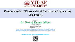
  • 1. Fundamentals of Electrical and Electronics Engineering (ECE1002) Presented By: Dr. Neeraj Kumar Misra Associate Professor Department of SENSE, VIT-AP University Google Scholar: https://scholar.google.co.in/citations?user=_V5Af5kAAAAJ&hl=en Research Gate profile: https://www.researchgate.net/profile/Neeraj_Kumar_Misra ORCHID ID: https://orcid.org/0000-0002-7907-0276
  • 2. Introduction: Dr. Neeraj Kumar Misra(Emp. ID: 70442) Associate Professor, SENSE ▪ Full-time Ph.D (Under TEQIP-II, A World Bank funded Fellowship, Gov. of India) ▪ Post Graduate Diploma in Artificial Intelligence and Machine Learning, from, NIT Warangle. ▪ B.Tech and M.Tech first class with distinction. ▪ Three International Patent granted (Validity 2028), Patent no. 2021105083, 2020103849, 2020102068 ▪ 9+ years of Teaching and Industry Experience ▪ Highest impact factor 8.907 paper published. ▪ Two times Young Achiever Awards in the domain of Quantum Computing ▪ The total 14 publications that were published in the SCI. ▪ Total 03 International books (ISBN: 978-3-659-34118-2, ISBN: 978-613-9-91317-6, ISBN: 978-620-2-01508-0) ▪ Google scholar citation 325, i10-15 and h-index-11. ▪ Funded Project completed 18 Lakh. ▪ Professional Member: IEEE, ACM, ISTE, IETE, WRC, InSc, IAENG, IRED. ▪ Editorial Board Member: ACTA Scientific, JCHE, IEAC, JEEE, IJCS ▪ Total no of Student Guided M.Tech: 10, Ph.D: 03 ▪ Most cited paper in the year 2019.
  • 3.
  • 4.
  • 6. Content ➢ Introduction to Electric Current a. Transient Current b. Steady Current ➢ Ohm’s Law: Resistance ➢ The internal resistance of the battery ➢ Numerical Based on Circuit theory
  • 8. Electric Current: Two Types 1. Transient Current (Very Short duration) 2. Steady Current (Slowly Movement): The charges flow in a steady manner e.g. Torch, Radio ➢ SI Unit- Ampere Def: If one coulomb of charge cross an area in one second then the current through that area in one ampere 1 ampere= 1 coulomb / 1 sec
  • 9. Electric Current: ➢The cause of flow of current through a conductor is potential difference applied across its ends. ➢Potential difference is created by battery. ➢The charge will flow in conductor if there is potential difference.
  • 10. Note: ➢ Electromotive force means work done by the battery per unit charge ➢ E and Fe decrease as free electron accumulate on positive terminal. ➢ Fb depends on the chemical composition of the battery.
  • 11. Internal Resistance of the battery R- External resistance r- internal resistance
  • 12. Ohm’s Law: ➢Ohm’s law given the relationship between electric current and potential difference. ➢Potential difference is created by battery. The current flowing through a conductor is directly proportional to the potential difference applied across it ends provided the temperature and other physical condition remain unchanged. Potential difference current Where R is the resistance of the conductor
  • 13. Q.1 Determine the current delivered by the battery and the potential difference across A and B Q2. In the given circuit internal resistance 0.1Ώ and EMF=2V and current I=2A, determine the potential difference and draw the circuit. Q3. When a cell is connected to 1 Ώ resistance the 1A current flows through the circuit and when 3 Ώ resistance is issued then 0.5A current flow then find the internal resistance of the cell. Numerical Question based on Electric Current A B
  • 14. Q.1 Determine the current delivered by the battery and the potential difference across A and B
  • 15. Q2. In the circuit internal resistance 0.1Ώ and EMF=2V and current I=2A, determine the potential difference and draw the circuit.
  • 16. Q3. When a cell is connected to 1 Ώ resistance the 1A current flows through the circuit and when 3 Ώ resistance is issued then 0.5A current flow then find the internal resistance of the cell.
  • 17. Q. Determine a. Current flow in the circuit (n cell) b. Current if R<<r c. Current if R>>r
  • 18. Q. Determine a. Current flow in the circuit (n cell) b. Current if R<<r c. Current if R>>r
  • 19. Q. Determine the current flow in the circuit and equivalent emf Q. Determine the equivalent emf in n-cell, neglect internal resistance
  • 20. Q. Determine the current flow in the circuit and equivalent emf
  • 21. Q. Determine the equivalent emf in n-cell, neglect internal resistance
  • 22. Q. Determine the equivalent emf in 3-cell, neglect internal resistance.
  • 23. Q. Find out a. Equivalent EMF in the given circuit b. If all the EMF are same and internal resistance are equal then find equivalent EMF
  • 24. Q. Find out a. Equivalent EMF in the given circuit b. If all the EMF are same and internal resistance are equal then find equivalent EMF
  • 25. Electric Current: The Junction Law or KCL, or Current Law ➢The sum of all the currents entering a junction in a circuit is equal to the sum of all the currents leaving it i entering = i leaving i outcoming = i outgoing ➢ KCL is based on the ‘conservation of charge’
  • 26. ➢In an electric circuit the algebraic sum of the current meeting at any junction in the circuit is zero. ➢Current toward junction means positive. ➢Current outwords junction means negative
  • 27. QUIZ Q1. For the circuit shown below calculate 𝑰𝟏+𝑰𝟐 𝑰𝟑+𝑰𝟒+𝑰𝟓
  • 28. QUIZ Q1. For the circuit shown below calculate 𝑰𝟏+𝑰𝟐 𝑰𝟑+𝑰𝟒+𝑰𝟓
  • 29. Concept of Open circuit and short circuit
  • 30. R V I Open circuit Short circuit Q. Fill this below table
  • 31. Nodal Analysis Q. Find the voltage across at 2ohm resistance using nodal analysis
  • 32. Q. Find the voltage across at 2ohm resistance using nodal analysis
  • 33. Mesh Analysis Q. Find the current I1 and I2 using mesh analysis
  • 34. Q. Find the current I1 and I2 using mesh analysis
  • 35. Find the current I1 and I2 using mesh analysis
  • 36.
  • 39. Vacant CB and filled VB Eg is very small as compared to insulator A large area of CB is overlapp with VB In VB electron has not sufficient energy to come to CB Si and Ge most common semiconductor Eg= 1.21 (for Si) = 0.78ev (for Ge) at 0K Large number of free electron exist which cause high conductivity and behave like metal No current flow (No free electron) At 0K electron can not move from VB to CB (Like a insulator) Resistivity is very high At room température few electron has sufficient energy to reach to CB Electron coming to CB known as free electron and the vaccanies created in VB known as hole
  • 40. Independent and Dependent Source Independent Source Dependent Source • The source which does not depend on any other quantity like voltage and current • Denoted by Circle • The source whose output value depends upon the voltage and current at some part of the circuit • Denoted by diamond
  • 41. Q. In the given circuit find out the dependent and independent source
  • 42. Dependent Source are broadly classified as 1. Current controlled voltage source (CCVS) 2. Voltage controlled voltage source (VCVS) 3. Current controlled current source (CCCS) 4. Votage controlled voltage source (VCCS)
  • 43. Current Controlled Voltage Source Voltage Controlled Current Source ➢ Value of dependent source is dependent on Ix ➢ If value of Ix change then value of dependent source is changes. ➢ R- Transresistance G- Transconductance
  • 44. Voltage Controlled Voltage Source (VCVS) Current Controlled Current Source (CCCS) ➢ Similarity in between VCVS and CCCS gives voltage and current source scaled value.
  • 45. Q. What will be the equivalent resistance between terminals P and Q of the ladder network Ans. Re=6 ohm
  • 46. Current to Voltage Source Transformation and Voltage to Current Source Transformation Q. Convert the given circuit into voltage source Q. Convert the given circuit into current source
  • 47. Q. Use source transformation to find the output voltage (𝑣o)
  • 48.
  • 51. Star and Delta Network ➢ In a Star network one common node or neutral point. ➢In a Delta network one closed loop and no any neutral point
  • 52. Star to Delta Conversion
  • 53. Delta to Star Conversion Only Change in Numerator
  • 54. Q1. Convert Star network into delta network Q2. Convert delta network into star network
  • 55. Q1. Find the voltage across 35ohm resistance using star delta conversion
  • 56.
  • 57.
  • 58. Q1. Find the equivalent resistance between A and B using star delta conversation
  • 59.
  • 60. Kirchof’s voltage law ➢ KVL deals with the conservation of energy around a closed circuit path. ➢ In a closed loop series path the algebric sum of all the voltage around any closed loop in a circuit is equal to zero. This is because a circuit loop in a closed conducting path so no energy is lost.
  • 61. Q. Find the voltage in the given circuit
  • 62.
  • 63. Q. Find the voltage across 10ohm resistance (Vx) using mesh analysis
  • 64.
  • 65.
  • 66. Q. Find the current in and the voltage across 2 ohm resistor
  • 67.
  • 68. Q. Find the voltage across 6ohm resistance
  • 69. Q. Find the voltage across 6ohm resistance
  • 70. Q. Obtain the equivalent resistance 𝑅ab for the given circuit and find current i.
  • 71.
  • 72.
  • 73.
  • 74. Q. Obtain the equivalent resistance at the terminals a-b for the given circuit.
  • 75.
  • 76.
  • 77. Q. Find the value of V in the circuit which contain CCVS
  • 78. Apply KVL in the network Method-1
  • 80. Q. Find the magnitude of total current through R1 and R2 if R1=10Ώ, R2=20 Ώ and V=50V
  • 81. Based on the current divider rule
  • 82. Q. Find the current in the 3 kΩ resistor by converting the current source to a voltage source
  • 83.
  • 84. Q. Apply KVL in the circuit and find the current in all the branches
  • 85. Apply KVL in the given network
  • 86. Q. Find the current delivered by the battery.
  • 87.
  • 88. Q. Find the voltage VCE and VAG in the given network
  • 89.
  • 90. Q. Find the equivalent resistance between terminal B and C
  • 91.
  • 92.
  • 93. Q. Use mesh analysis to determine i1, i2, i3 and i4.
  • 94.
  • 95. 1. Unidirectional Elements: When an element properties and characteristic are independent of the current flow direction then the element is called a unidirectional element. Concept of Unidirectional and Bidirectional Elements 2. Bidirectional Elements: When an element properties and characteristic depends on the current flow direction then the element is called a bidirectional element.
  • 96. Statement: In any linear bi-directional circuit having more number of active and passive elements can be replaced by a single equivalent circuit consisting of an equivalent voltage source in series with equivalent resistance (Rth) Thevenin's Theorem
  • 97. Q. In the given network find the current across load resistance (RL=10ohm) using the Thevenin theorem. Hint: 1. Remove the load resistance (RL) and find the open circuit voltage (Voc or Vth) 2. Deactivate the independent source and find Rth of the source side looking through the circuitry load terminal. 3. Reconnect RL across the load terminal. 4. Find the I across load resistance Ans I = 0.774 Amp
  • 98. Step 1: Calculation of Vth or Voc Remove the load resistance (RL) and find the open circuit voltage (Voc or Vth) Step 2: Calculation of Rth Deactivate the independent source and find Rth of the source side looking through the circuitry load terminal.
  • 99. Step 3: Reconnect RL across the load terminal.
  • 100. Q. Find the current across 2ohm resistance in the given network using Thevenin theorem. Ans I= 25/3 Amp
  • 101.
  • 102.
  • 103. Q. Using Thevenin’s theorem calculate the current flowing through the load resistance RL connected across the terminals A and B as shown below. Hint: 1. Remove the load resistance (RL) and find the open circuit voltage (Voc or Vth) 2. Deactivate the independent source and find Rth of the source side looking through the circuitry load terminal. 3. Reconnect RL across the load terminal. 4. Find the I across load resistance Ans I= 0.193 Amp
  • 104.
  • 105.
  • 106. Q. Use Thevenin’s theorem to calculate the current flowing through the 5 Ω resistor in the circuit shown below Ans I= 0.8 Amp
  • 107.
  • 108.
  • 109. Maximum Power Transfer Theorem Statement ▪ It states that maximum power is transferred to the load when the load resistance equals the Thevenin resistance (RL = RTh)
  • 110.
  • 111.
  • 112. Q. Find the value of RL for maximum power transfer in the circuit and also find the maximum value of power.
  • 113.
  • 114.
  • 115.
  • 116. Superposition Theorem Statement: “In a linear network containing more than one independent source and dependent source, the resultant current/voltage in any element is the algebraic sum of the current/voltage that would be produced by each independent sources acting alone all other independent sources being replaced by their respective internal resistance.”
  • 117. Q. Determine the current through the 10ohm resistance using the superposition theorem. Hint: 1. Two independent sources (10V and 4A source) which means analysing the circuit two times. 2. First: 10V acting alone and 4A is open circuit. 3. Second: 4A current source acting alone and 10V battery is a short circuit
  • 118. 1. 10V source acting alone To find Ix (Fig 2) Apply the current division rule (Fig 3)
  • 119. 2. 4A source acting alone Current division rule (fig 2) Current division rule (fig 1) By superposition theorem
  • 120. Unit-II Alternating Current (AC) Direct Current (DC An alternating current is that current whose magnitude changes continuously with time and direction reverses periodically. A direct current is that current which flows with a constant magnitude in the same direction Eg. Electricity supply in home is alternating current In mobile or inverter provide the DC current
  • 121. Average value of AC over one complete cycle
  • 122. Mean or average value of AC It is defined as the value of direct current which sends the same charge in a circuit in the same time as sent by the given alternating current in its half time period.
  • 126. Q. Find the voltage V in the circuit using the superposition theorem
  • 127. Step-1 Source 5V acting Step-2 Source 3A acting Current division rule Using superposition theorem
  • 128. Q. Find the current io in the circuit using the superposition theorem.
  • 129. Step-1 Source 4A acting Loop-1 Loop-2 Loop-3
  • 130. Step-2 Source 20V acting Using superposition theorem
  • 131. SuperMesh ➢When a current source is present between two meshes then we remove the branch having the current source and remaining loop is known as supermesh.
  • 132. Q. Find the value of current in 1ohm resistance
  • 133.
  • 134. Q. Find the current through the 10ohm resistance
  • 135.
  • 136. Q. Find the current in all the branch and current flow in 2ohm resistance using supermesh analysis
  • 137.
  • 138. Terminology: RMS value, Average Value, Form Factor Form factor= 𝑹𝑴𝑺 𝑽𝒂𝒍𝒖𝒆 𝑨𝒗𝒆𝒓𝒂𝒈𝒆 𝑽𝒂𝒍𝒖𝒆 Q. Calculate the following parameters RMS value, Average Value, Form Factor in the given waveform
  • 139.
  • 140. Q. For the triangular waveform which is shown in the below figure, determine the RMS value, Average Value, Form Factor and Peak Factor
  • 141.
  • 142.
  • 143. Q. For the trapezoidal voltage waveform which is shown in the below figure, determine the RMS value, Average Value, Form Factor and Peak Factor
  • 144.
  • 145.
  • 146. J-Operator ➢When dealing with frequency-dependent sinusoidal sources, we need to use complex numbers along with real numbers
  • 147.
  • 148.
  • 149.
  • 150. Concept of Impedance and Admitance 1. Pure resistive circuit
  • 151. Phasor Diagram: 1. I and V are represented as phasor 2. Rotation in anticlockwise direction
  • 152. AC circuit with capacitor only
  • 153. AC circuit with capacitor only
  • 154. AC circuit with capacitor only
  • 155. AC circuit with capacitor only
  • 156. AC circuit with capacitor only
  • 157. AC circuit with Inductance only
  • 158. AC circuit with Inductance only
  • 159. AC circuit with Inductance only
  • 161. Live Quiz-1 Q.1 Which of the following is not ac waveform? a) sinusoidal b) square c) constant d) triangular Q.2 The expression for capacitive reactance is given by _____________ a) 1/ωC b) ω L c) ωC d) None of the above Q3. Which one of the following voltages is obtained from a generator? a. AC voltage b. DC voltage c. Both a and b d. None of the above
  • 162. Q. Find out these values in RC Circuit Z, VR, Vc, i, i0, tan φ
  • 163. Q. Find out these values in RL Circuit Z, VR, VL, i, i0, tan φ
  • 164. Q. Find out these values in LC Circuit Z, VC, VL, i, i0, tan φ
  • 165. Q. Find out these values in LC Circuit Z, VC, VL, i, i0
  • 166. Q. Find out these values in LC Circuit Z, VC, VL, i, i0, and plot Z versus ω
  • 167. Q. Find out these values in LC Circuit Z, VC, VL, i, i0, and plot Z versus ω
  • 168. Q. Find out these values in LC Circuit Z, VC, VL, i, i0, and plot Z versus ω
  • 169. Q. Find out these values in series RLC Circuit Vnet, Z, tan φ, i, i0, resonance condition, plot i0 versus ω
  • 170. Q. Find out these values in series RLC Circuit Vnet, Z, tan φ, i, i0, resonance condition, plot i0 versus ω
  • 171. Q. Find out these values in series RLC Circuit Vnet, Z, tan φ, i, i0, resonance condition, plot i0 versus ω
  • 172. Q. Find out these values in series RLC Circuit Vnet, Z, tan φ, i, i0, resonance condition, plot i0 versus ω
  • 173. Q. Find out these values in series RLC Circuit Vnet, Z, tan φ, i, i0, resonance condition, plot i0 versus ω
  • 174. Q. Find out these values in parallel RLC Circuit Vnet, Z, tan φ, i, i0, resonance condition, plot i0 versus ω
  • 175. Concept of Power, Average power, real power, virtual power and power factor in AC circuit * Power in AC circuit Pm = Vm x Im (Where Vm and Im represent instantaneous value) * Average power Pavg= (This is one method to calculate average power, but it is complex) Instantaneous value of V Instantaneous value of I Instantaneous value of P
  • 176. Concept of Power, Average power, real power, virtual power and power factor in AC circuit
  • 177. Concept of Power, Average power, real power, virtual power and power factor in AC circuit
  • 178. Q1. Find out the impedance of the following circuit Q2. Find out the Z, I, power factor, Voltage phasor diagram for the given circuit
  • 179. Live Quiz Q. Find the node voltages (V1 and V2) of the following circuit.
  • 180.
  • 181. Concept of Virtual Power and Real Power ➢Virtual power is not real power ➢In virtual power phase difference is not considered. ➢In real power phase difference is considered. ➢In real power phase angle is considered ➢If the phase angle is increased then the power factor increases and vice versa
  • 182. Concept of Virtual Power and Real Power
  • 183. Average Power in Pure Resistive element
  • 184. Average Power in Inductive and Capacitive element
  • 185. Average Power in Inductive and Capacitive element
  • 186. Average Power in Pure resistive element
  • 187. Average Power in RLC circuit
  • 188. Concept of Power Factor 1. Power factor (Pf) is the cosine of the phase difference between voltage and current. 2. Pf is dimensionless. ➢ Pf is the cosine of the angle of the load impedance.
  • 189. Concept of Complex Power ➢ Voltage and current must be in phasor form ➢ Complex power (S) absorbed by ac load
  • 190. Concept of Complex Power ➢ P is the real part of a complex number ➢ Q is the imaginary part of a complex number
  • 191. Concept of real power and reactive power Real Power: Real power is the useful power or average power delivered to a load. Load dissipate the power is known as real power. Reactive Power: Reactive power is the power to delivered to source to load and load to source and it not dissipate by load.
  • 192. Reactive power value in resistive, capacitive and inductive load Pure resistive Capacitive Load Inductive Load
  • 193. Power Triangle, and Impedance Triangle Power Triangle Impedance Triangle
  • 194. Q1. If the load impedance angle is 45 degrees find the power factor. Q2. Find the instantaneous power and the average power absorbed Q3. Find the average power applied by the source and the average power absorbed by the resistor
  • 195. Q1. If the load impedance angle is 45 degrees find the power factor. Q2. Find the instantaneous power and the average power absorbed
  • 196. Q3. Find the average power applied by the source and the average power absorbed by the resistor
  • 197. Q3. The voltage across a load is 𝒗(𝒕) = 𝟔𝟎𝒄𝒐𝒔(𝝎𝒕 − 𝟏𝟎°)𝑽 and the current through the element in the direction of the voltage drop is 𝒊(𝒕) =𝟏. 𝟓𝒄𝒐𝒔(𝝎𝒕 + 𝟓𝟎°)𝑨 Find: (a) The complex and apparent powers, (b) The real and reactive powers, (c) The power factor and the load impedance.
  • 198.
  • 199. Valance Band Conduction Band The valence band consists of the electrons that lie in the outermost shell or valence shell of the atom. The conduction band consists of the free electrons that take part in the process of conduction. The valence band lies below the Fermi level. The conduction band lies above the Fermi level. When external energy is given to the electrons in the valence they leave the valence band. When external energy is given to the electrons they leave the valence band and reach the conduction band. There is no flow of current due to the electrons present in the valence band. The free electrons present in the conduction band are free to move anywhere within the volume of the solid, therefore current flows due to these electrons. Due to the presence of electrons valence band is partially or completely filled. The conduction band is either empty or partially filled.
  • 200. Remember ➢ Hole is a seat of positive charge which is produced when an electron breaks away from a covalent bond in a semiconductor. ➢ Hole carries a unit positive charge. ➢ Hole has the same charge as that of electron. ➢ Energy of a hole is high as compared to that of electron. ➢ The mobility of hole is smaller ➢ The three acceptor impurities are Aluminium, Indium, and gallium. ➢ The three donor impurities are Phosphorus, Antimony, and Arsenic. ➢ In n-type semiconductor: Both electrons and holes exist as charge carriers in n-type semiconductor. However, electrons are majority charge carriers while holes are minority charge carriers. Silicon is preferred to germanium in the manufacture of semiconductor devices due to following reasons. ➢ The leakage current in silicon is very small as compared to that of germanium. ➢ In case of silicon, the leakage current is less effected with temperature as compared to germanium. ➢ The working temperature of silicon is more than that of germanium. The structure of germanium gets destroyed at a temperature of about 100 °C but silicon can be operated upto about 200°C.
  • 202. Intrinsic Semiconductor Extrinsic Semiconductor Pure forms of semiconductors Extrinsic semiconductors are made by adding some impurity to the pure form of semiconductors. They exhibit poor electrical conductivity. Electrical conductivity in the case of extrinsic semiconductors is significantly high as compared to intrinsic semiconductors. Intrinsic semiconductors, the number of free electrons in the conduction band is equal to the number of holes in the valence band. The number of electrons and holes are not equal in extrinsic semiconductors and depends on the type of extrinsic semiconductor. The electrical conductivity of intrinsic semiconductors depends only on the temperature. The electrical conductivity of extrinsic semiconductors depends on the temperature as well as the amount of doped impurity. In intrinsic semiconductors, the Fermi energy levels lie in the middle of the valence and conduction band. In extrinsic semiconductors, the Fermi level shifts towards the valence or conduction band. Examples include the crystalline forms of pure silicon or germanium. Examples include Silicon (Si) and germanium (Ge) crystals with impurity atoms of As, Sb, P, etc., or In, B, Al, etc.
  • 203.
  • 204. P-type semiconductor N-type semiconductor P-type semiconductors are formed due to doping of elements of group III i.e. Boron, Aluminium, Thallium, etc. N-type semiconductors are formed due to doping of elements of group V i.e. Nitrogen, Phosphorus, Arsenic, Antimony, Bismuth, etc. Holes are the majority carriers in P-type semiconductors. Electrons are the majority carriers in n-type semiconductors. Electrons are the minority carriers in P-type semiconductors. Holes are minority carriers in N-type semiconductors. The fermi energy levels of these materials lie between the impurity energy level and the valence band. The Fermi levels of these materials lie between the impurity energy level and the conduction band. The movement of majority carriers is from higher potential to lower potential. The movement of majority carriers is from lower potential to higher potential. In P-type semiconductors, hole density is greater than the electron density. Nh > Ne Electron density is much greater than the hole density for the n-type semiconductors. Ne > Nh
  • 206. Extrinsic semiconductor: N type semiconductor
  • 207. Extrinsic semiconductor: P type semiconductor
  • 208. Extrinsic semiconductor: N and P -type semiconductor
  • 209. P-N Junction diode Need to learn this concept 1. P-N Junction diode 2. Depletion region 3. Immobile charge 4. Potential barrier 5. Diffusion current 6. Drift current 7. Forward biased 8. Reverse biased
  • 211. Depletion Region ➢The region on either of the junction which becomes depleted (free) of the mobile charge carrier is called the depletion region. ➢Positive and Negative ions fixed in their position are known as the Depletion region.
  • 212. Potential Barrier (Vb) ➢The potential difference created across the PN junction due to diffusion of electron and hole is called potential barrier ➢Vb= 0.3V (Ge), 0.7V (Si) ➢Deflection width is very small: 10-6 m Due to the high electric field, electrons do not cross the barrier similar hole also not cross the barrier.
  • 213. Diffusion Current ➢ Due to the difference in concentration of charge carrier hole and electron start diffusion from one side to another side. This diffusion result is an electric current from P-side to N-side is known diffusion current.
  • 214. Drift Current ➢ Drift current flow due to thermal energy, collision, covalent bond break, electron-hole pair created. Due to these above effect hole move towards P-side and electron move towards n-side. ➢ Drift current and diffusion current are in opposite direction
  • 215. Forward and Reversed Biased Forward Biased Reversed Biased In forward biased positive terminal of the battery is connected to the P-Type and the negative terminal of the battery is connected to N- Type In reversed biased positive terminal of battery is connected to N- Type and negative terminal of battery is connected to P-Type Forward biased opposes the potential barrier and for V>Vb and forward current is setup across the junction. Reverse biased support the potential barrier and no current flow across the junction due to diffusion of majority carrier. Width of the depletion region decrease. That means a large current will flow in the device. Width of the depletion region increase. That means very small reverse current may exist (Microampere) Knee (Voltage): The voltage at which the current start to increase. Breakdown voltage: Reverse voltage in which the breakdown of the semiconductor occurs.
  • 216. Forward and Reversed Biased Forward Biased Reversed Biased Small current in microampere due to the motion of the few thermally generated minority carriers (Electron in p region and hole in n-region) whose motion is added by the applied voltage.
  • 217. Q. Two ideal diode are connected in parallel. What is the current flow in the circuit?
  • 218. Q.1 Find VD, VR, and ID in the given circuit. Q2. Find V0, and ID in the given circuit. Q3. Find ID, VD2, and V0 in the given circuit. Q4. Find V0 in the given circuit Problem Based on Diode
  • 219. Q5. Find V0 in the given circuit Problem Based on Diode
  • 220. Q5. Find V0 in the given circuit Problem Based on Diode
  • 221. ➢ When a reverse bias is increased the electric field at the junction also increases. At some stage, the electric field becomes so high that it breaks the covalent bonds creating electron, hole pairs. ➢ Thus a large number of carriers are generated. This causes a large current to flow. This mechanism is known as Zenor breakdown. ➢ Zener diode is used in reverse biased, and it is used for voltage regulation. Zenor breakdown.
  • 222. ➢ At high reverse voltage due to a high electric field, the minority charge carriers while crossing the junction acquire very high velocities. ➢ These by collision breaks down the covalent bonds, generating more carriers. A chain reaction is established giving rise to high current. This mechanism is called avalanche breakdown. ➢ The avalanche breakdown occurs in a lightly doped junction. Avalanche breakdown
  • 223. Difference between Zener and Avalanche Breakdown
  • 224. Zenor Diode as Voltage Regulation ➢ Voltage across Zenor- Vz ➢ Purpose of Zenor diode To get a constant dc voltage from the unregulated input of a rectifier. ➢ The input voltage may vary but the output regulated
  • 225. Zenor Diode as Voltage Regulation Q. The reverse breakdown voltage of a zenor diode is 5.6V in the given circuit. Find the current IL through the load resistance.
  • 226.
  • 227. Zenor Diode as Voltage Regulation Q. Figure shows a DC voltage regulator circuit with a zener diode of breakdown voltage=6V. If the unregulated input voltage between 10V to 16V then what is the maximum zener current?
  • 228. Zenor Diode as Voltage Regulation
  • 229. Zenor Diode as Voltage Regulation Q. A 5.0V stabilized power supply is required to be produced from a 12V DC power supply input source. The maximum power rating PZ of the Zener diode is 2W. Using the Zener regulator circuit above calculate: a) The maximum current flowing through the Zener diode. b) The minimum value of the series resistor, RS c) The load current IL if a load resistor of 1kΩ is connected across the Zener diode. d) The Zener current IZ at full load.
  • 230.
  • 232. In half wave rectifier diode conduct in positive half cycle and does not conduct during the negative half cycle. Hence AC is converted by diode into unidirectional pulsating DC. This action is known as half wave rectifier. Diode as the Half Wave Rectifier
  • 233. In full-wave rectifier two p-n junction diode D1 and D2 are used. Diode as the Full Wave Rectifier
  • 234. Bridge Rectifier ➢ During positive cycle D1 and D2 forward bias (Closed Circuit) ➢ During negative cycle D3 and D4 forward bias (Closed Circuit)
  • 235. Ripple Factor ➢ The ripple factor measures the percentage of ac components in the rectified output. ➢ The ideal value of ripple factor should be zero. rms value of ac component of output Ac value of output Ripple factor of half wave rectifier=1.21 or 121% Efficiency of half wave rectifier=40.6%
  • 236. Q. What should be the value of R such that maximum power transfer can place in the following circuit? Find the maximum power transferred from the rest of the network to the R. Maximum Power Transfer Theorem
  • 237. Q. Find the voltage across 10ohm resistance (Vx) using mesh analysis
  • 238.
  • 239.
  • 240. Q. The voltage across a load is 𝒗(𝒕) = 𝟔𝟎𝒄𝒐𝒔(𝝎𝒕 − 𝟏𝟎°)𝑽 and the current through the element in the direction of the voltage drop is 𝒊(𝒕) =𝟏. 𝟓𝒄𝒐𝒔(𝝎𝒕 + 𝟓𝟎°)𝑨 Find: (a) The complex and apparent powers, (b) The real and reactive powers, (c) The power factor and the load impedance.
  • 241.
  • 242. Q. Find the current I in the load resistance using nodal analysis
  • 243. Q. Determine the dc resistance level for the diode a. ID= 2 mA b. ID=20mA c. VD=-10V
  • 244. Q. For the trapezoidal voltage waveform which is shown in the below figure, determine the RMS value, Average Value, Form Factor and Peak Factor
  • 245.
  • 246.
  • 247. Q. For the triangular waveform which is shown in the below figure, determine the RMS value, Average Value, Form Factor and Peak Factor
  • 248.
  • 249.
  • 250. Q. Using Thevenin’s theorem calculate the current flowing through the load resistance RL connected across the terminals A and B as shown.
  • 251.
  • 252. Q. Find the current io in the circuit using the superposition theorem.
  • 253. Step-1 Source 4A acting Loop-1 Loop-2 Loop-3
  • 254. Step-2 Source 20V acting Using superposition theorem
  • 255. Q. Over what range of input voltage will the zener circuit shown in Figure below maintain 30 V across 2000 Ω load, assuming that series resistance R = 200 Ω and zener current rating is 25 mA ?
  • 256. Q. Over what range of input voltage will the Zener diode maintain 30V across 2000ohm, assuming that series resistance R=200ohm and Zener diode rating is 25mA.
  • 257.
  • 258. Bipolar Junction Transistor (BJT) ➢ There are three terminals of BJT. These terminals are known as collector (C), emitter (E) and base (B) ➢ All regions (E, B and C) have different thicknesses and doping levels. ➢ Emitter is used to emit all the charges and Collector is used to collect all the charges.
  • 259. Terminal Doping Size Emitter Heavily doped Supplies/Emit majority charge carrier Thinner than collector And Thicker than base Base Lightly doped Very thin Passes charge carriers to collector Collector Moderate doped Thickest in size Collect or remove majority charge carrier coming from emitter
  • 260. Working of PNP Transistor
  • 261. Transistor Configuration A transistor can be connected in the circuit in the following three ways ➢ Common base (CB) ➢ Common emitter (CE) ➢ Common collector (CC) Common base (CB) configuration:
  • 262. Input and Output Characteristics of Common base (CB) configuration: a. Input Characteristics:
  • 263. Input and Output Characteristics of Common base (CB) configuration: a. Output Characteristics:
  • 264. Transistor Biasing: Note: In Forward biased: p must be connected to the Positive terminal n must be connected to the negative terminal In Reversed biased: n must be connected to the Positive terminal p must be connected to the negative terminal forward-reverse bias.
  • 265. Direction of Current in PNP and NPN Transistor forward-reverse bias.
  • 266. Diode representation of Transistor
  • 267. Transistor Biasing ➢Transistor Biasing is the process of setting a transistor DC operating voltage or current conditions to the correct level so that any AC input signal can be amplified correctly by the transistor. ➢Biasing is used to set the Q-point. ➢The process of applying dc voltage across the different junctions of the transistor is called biasing.
  • 268. Transistor Biasing 1. Active: Used for amplification 2. Saturation: Ic is independent of base current IB Transistor work as switch and closed 3. Cut-off: Emittter terminal not emit any charge and transistor work as open switch 4. Inverted: Emitter is heavily doped and A collector is moderately doped This region action is very poor.
  • 270. Q-Point ➢ When a line drawn over the output characteristic curve, the line makes a contact at a point this is known as the operating point or Q-point.
  • 272. Biasing Types 1. Fixed bias 2. Voltage divider bias 3. Collector to base bias
  • 276. Q. Calculate the emitter current, IE and collector voltage, VC.
  • 277. Op-Amp (Operational Amplifier) ➢ Op-Amp is an IC to amplify the input voltage with Av (Gain) times and provides a high output voltage. ➢Op-Amp is the voltage-controlled, voltage source device. ➢Gain of Op-Amp varies with a different type of Op-Amp IC.
  • 278. Symbol of Op-Amp ➢ For high amplification, the gain must be high ➢ For Op-Amp Av (gain) is very high.
  • 279. Symbol of Op-Amp ➢ Input resistance Ri= (Means it open circuit and no drop on the input side) ➢ Output resistance R0 = 0 (Means gain to be maintained and no drop, then the output voltage is very high.
  • 281. Open-Loop Gain= for (Ideal Op-Amp)
  • 282. Op-Amp Types 1. Inverting 2. Non-inverting 3. Differential 1. Inverting: Invert the input signal 2. Non-inverting: The input signal is not inverted
  • 284. Inverting amplifier with feedback ➢ Negative feedback means output voltage connected to the negative terminal
  • 286. Numerical Questions based on inverting and non-inverting amplifier Q1. Determine the voltage gain of the op-amp for the given circuit
  • 287. Q1. Determine the voltage gain of the op-amp for the given circuit
  • 288. Numerical Questions based on inverting and non-inverting amplifier Q2. Determine the output voltage of the 3-input adder circuit as shown below
  • 289. Q2. Determine the output voltage of the 3-input adder circuit as shown below
  • 290. Numerical Questions based on inverting and non-inverting amplifier Q3. Determine the output voltage of the op-amp for the given circuit
  • 291. Q3. Determine the output voltage of the op-amp for the given circuit
  • 292. Numerical Questions based on inverting and non-inverting amplifier Q4. Determine the output voltage of the op-amp for the given circuit
  • 293. Q4. Determine the output voltage of the op-amp for the given circuit
  • 294. Numerical Questions based on inverting and non-inverting amplifier Q5. Determine the output voltage of the op-amp for the given circuit
  • 295. Q5. Determine the output voltage of the op-amp for the given circuit
  • 296. Common Mode Rejection Ratio (CMRR) Common mode Signal Differential mode signal
  • 297. Common Mode Rejection Ratio (CMRR) Differential Mode Common mode input