Downloaded 104 times
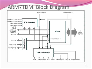
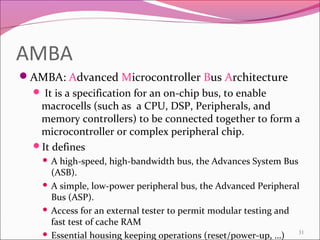
![Memory Interface
32-bit address bus
32-bit data bus
D[31:0]: Bidirectional data bus
DIN[31:0]: Unidirectional input bus
DOUT[31:0]: Unidirectional output bus
Control signals
Specified the size of the data to be transferred and the
direction of the transfer
7](https://image.slidesharecdn.com/arm-hardware-090429041302-phpapp02/85/ARM7TDM-7-320.jpg)
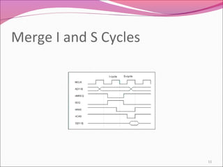
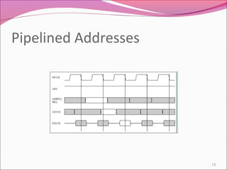
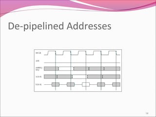
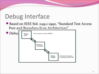
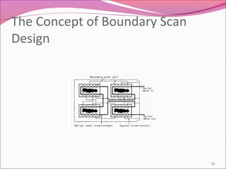
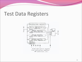
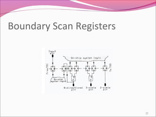
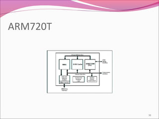

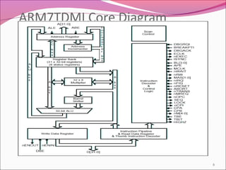
The document describes the ARM7TDMI processor core. It is a 32-bit RISC processor capable of executing 16-bit Thumb instructions. It features a JTAG debugging interface, multiplier, and support for embedded emulation. It has a three-stage pipeline and interfaces with memory using different bus cycles.