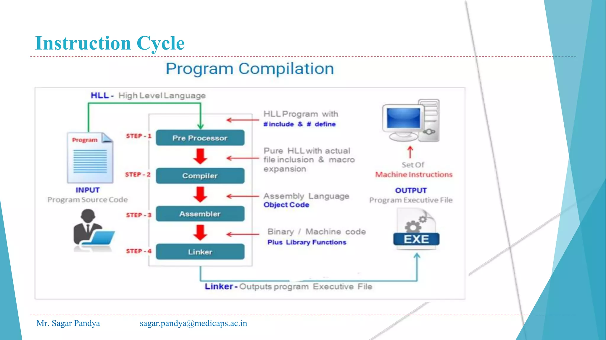
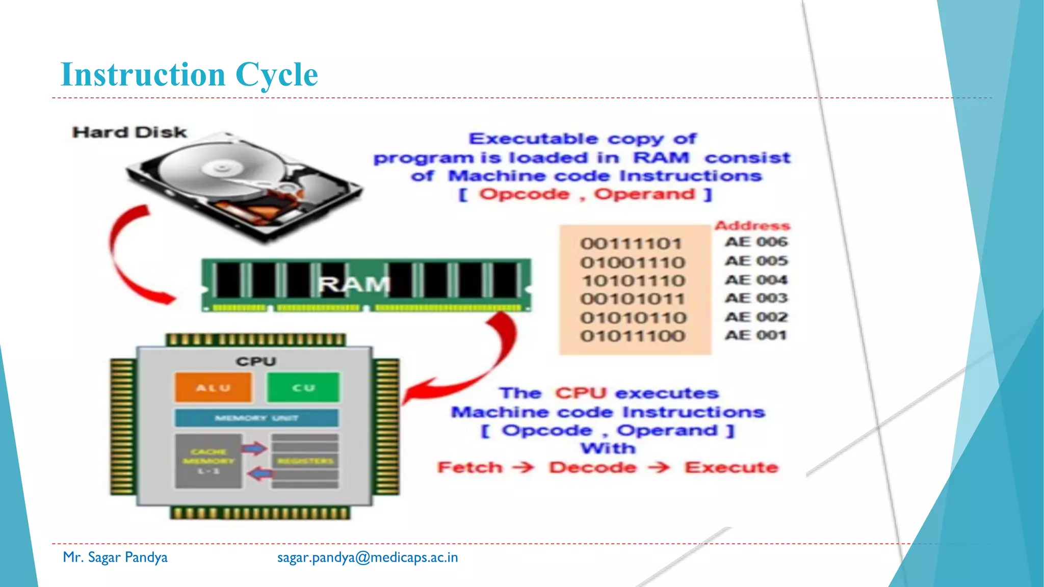
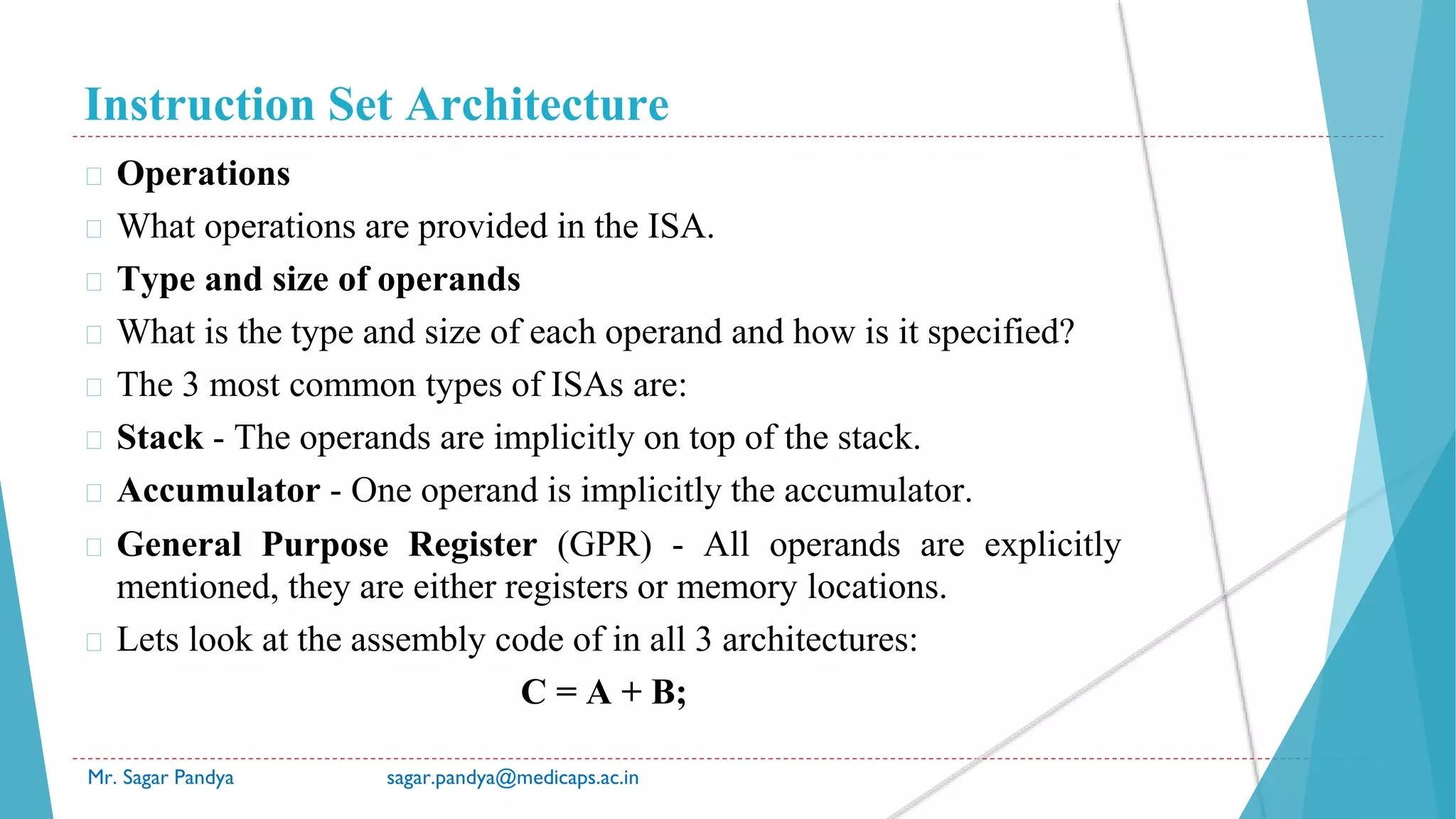
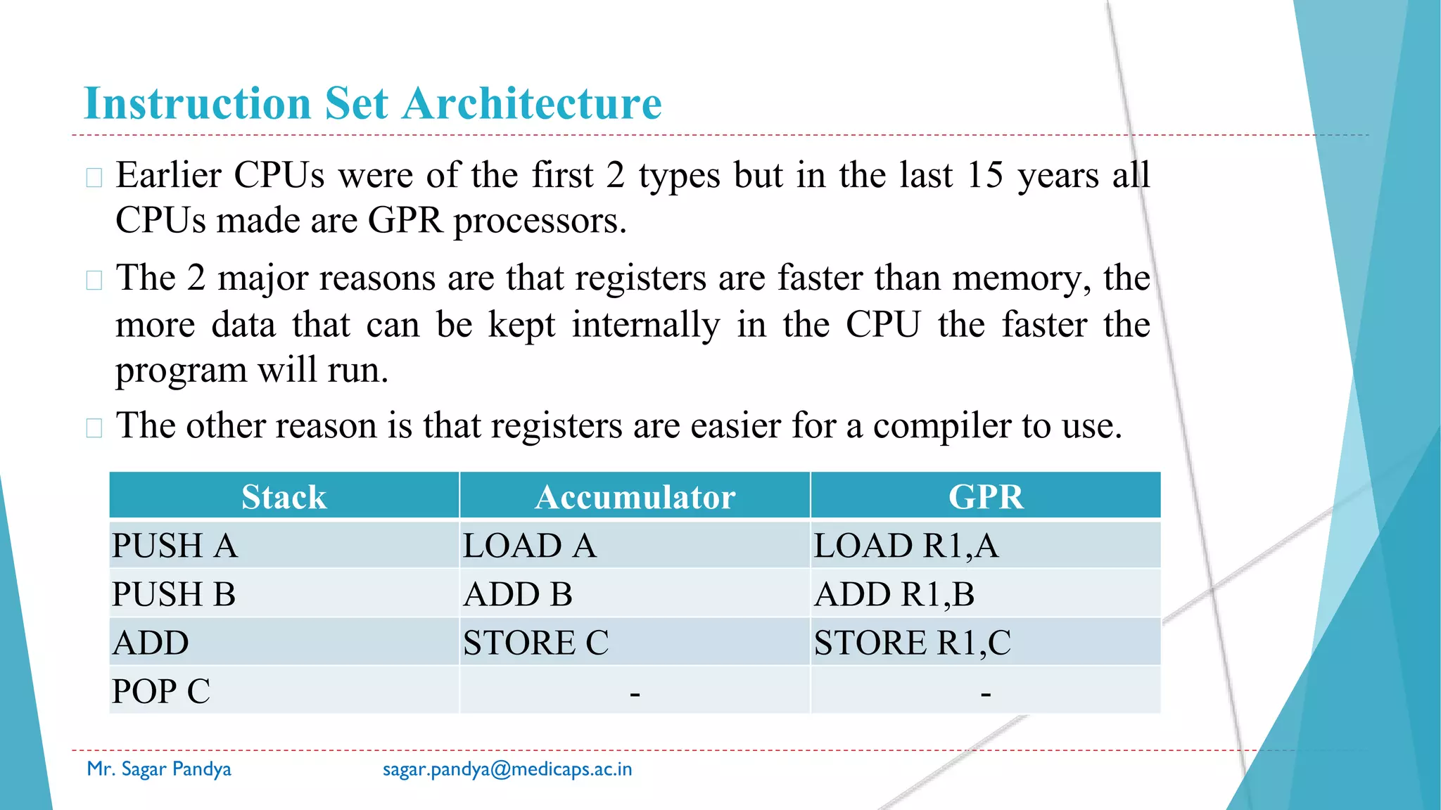
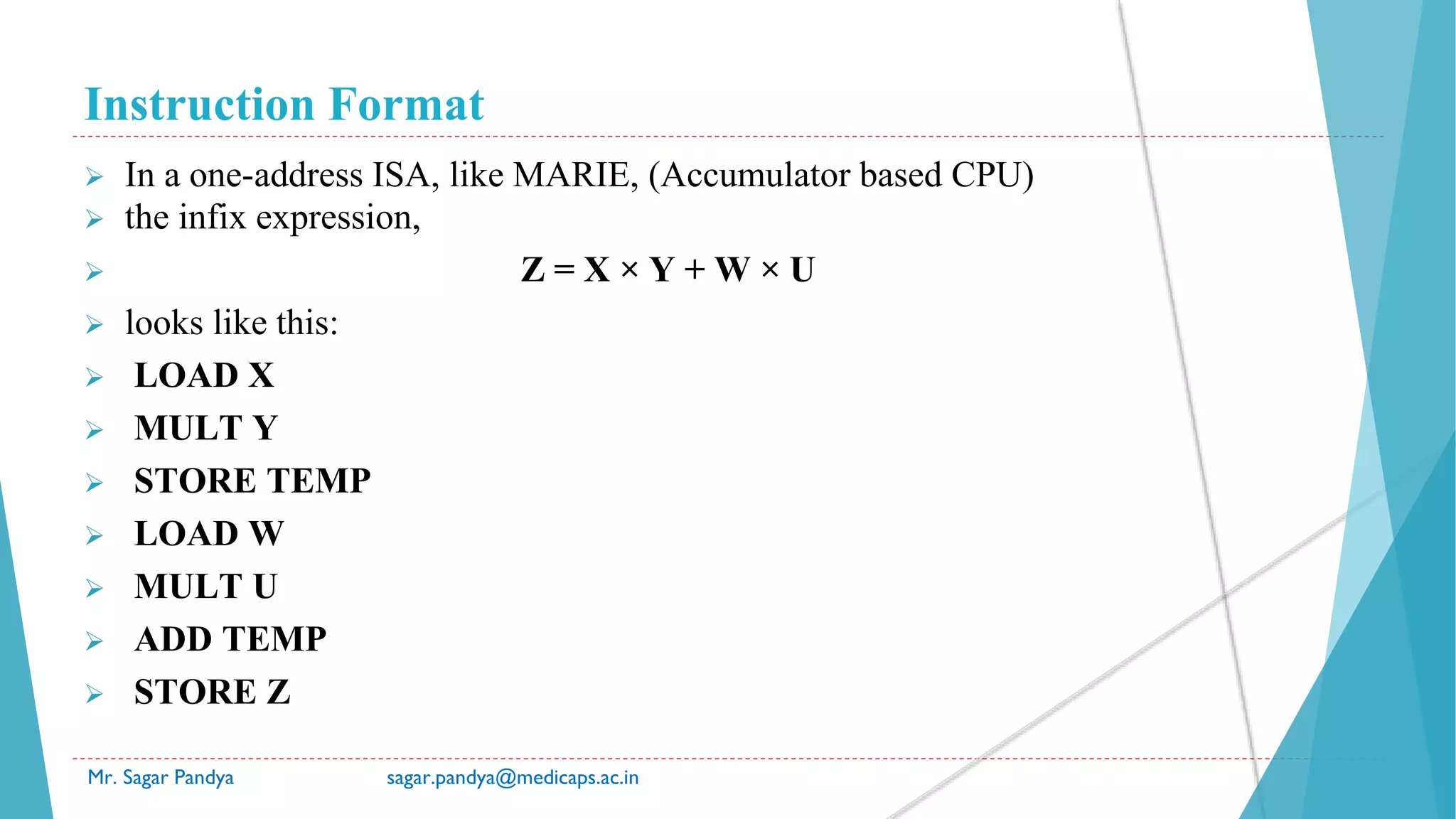
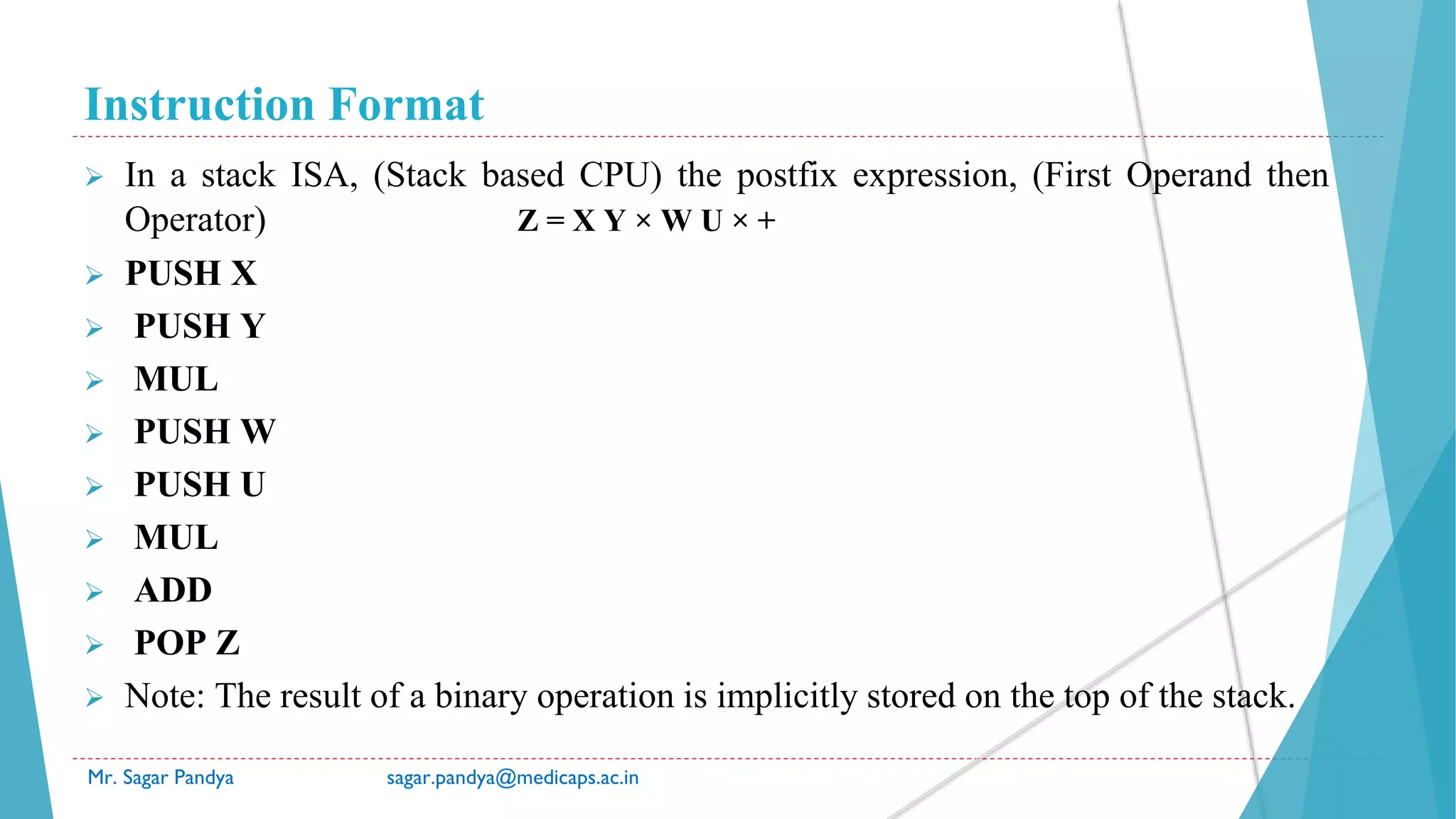
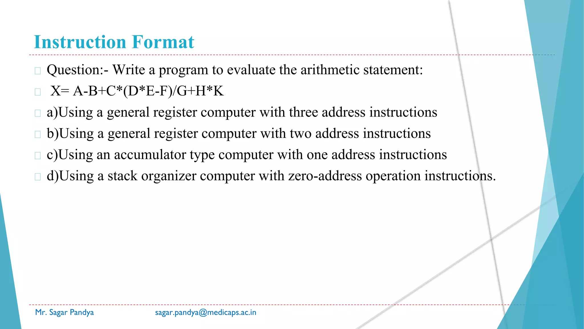
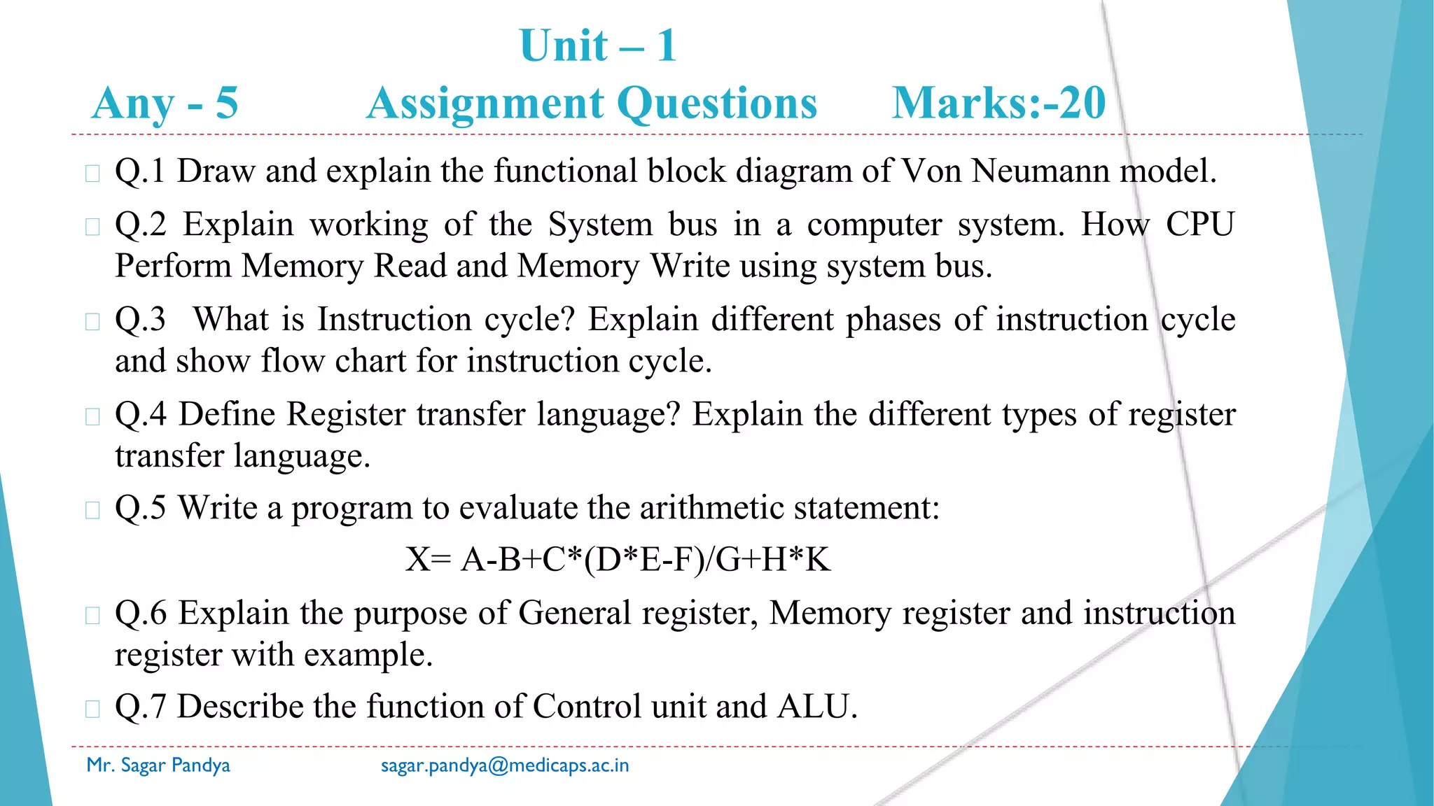
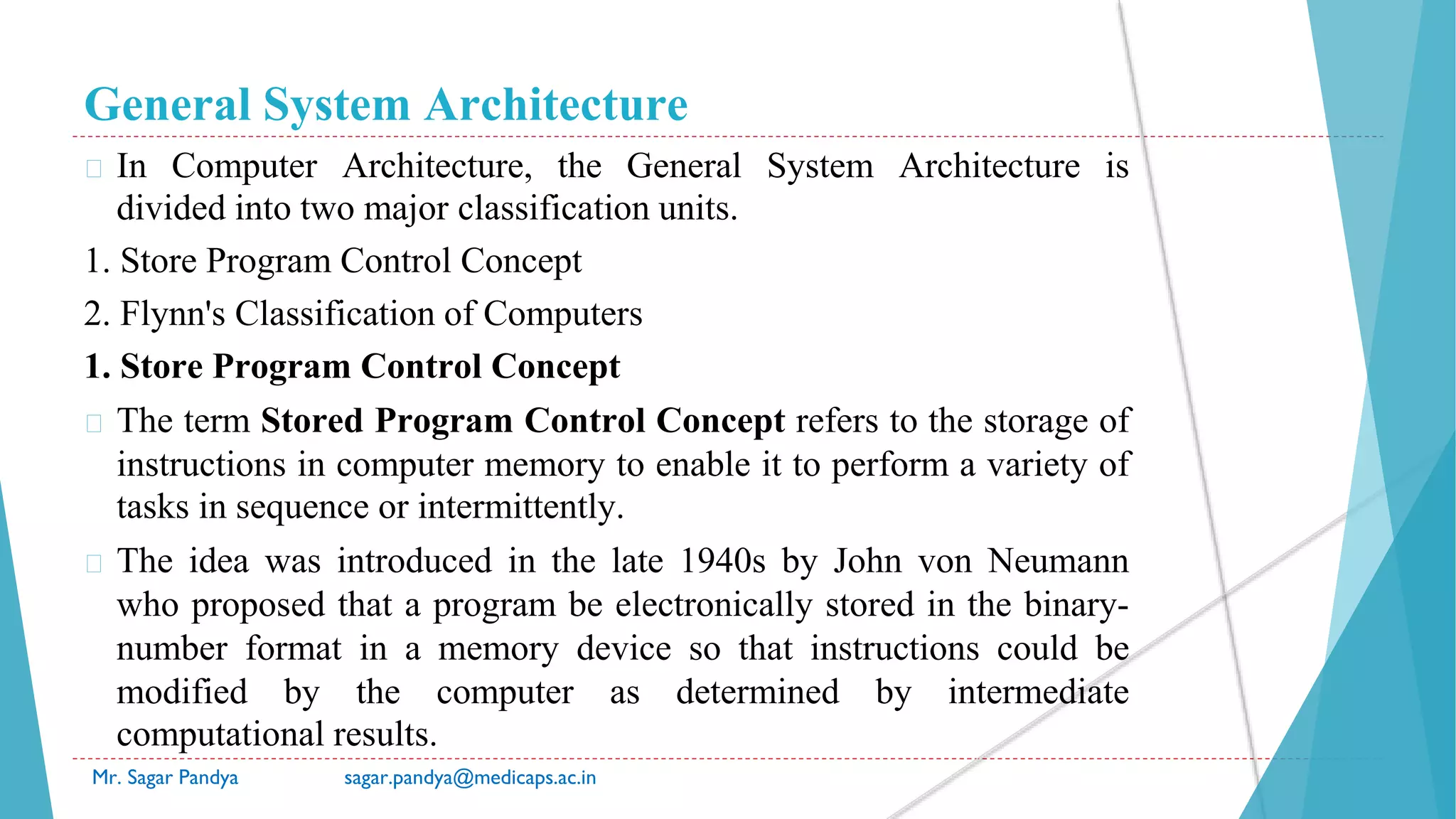
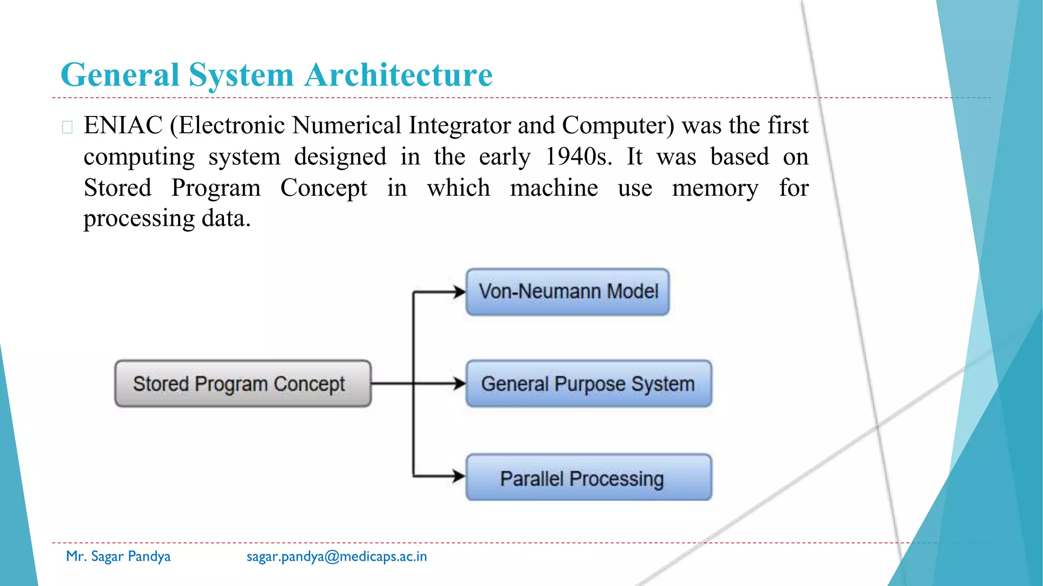
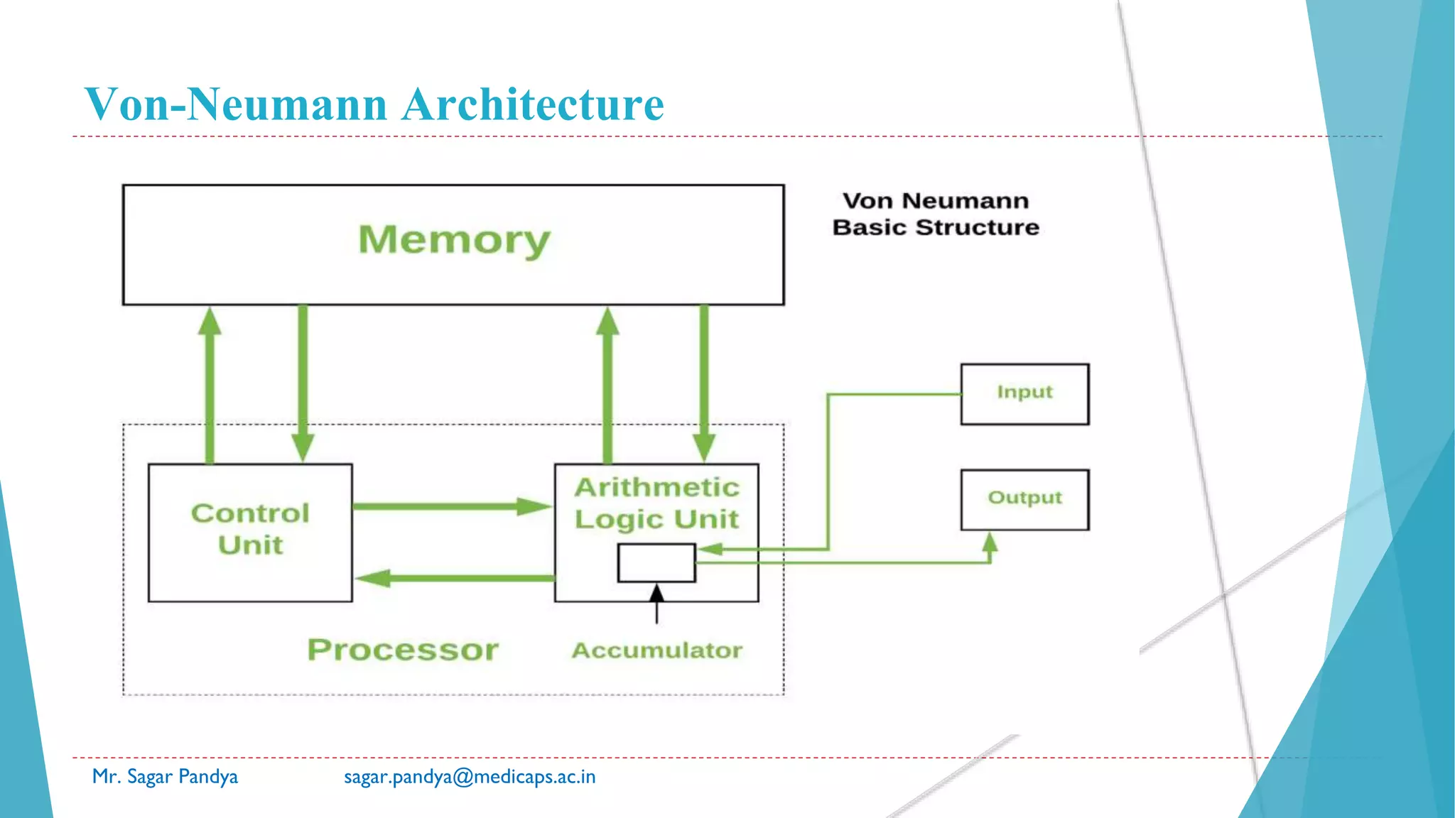
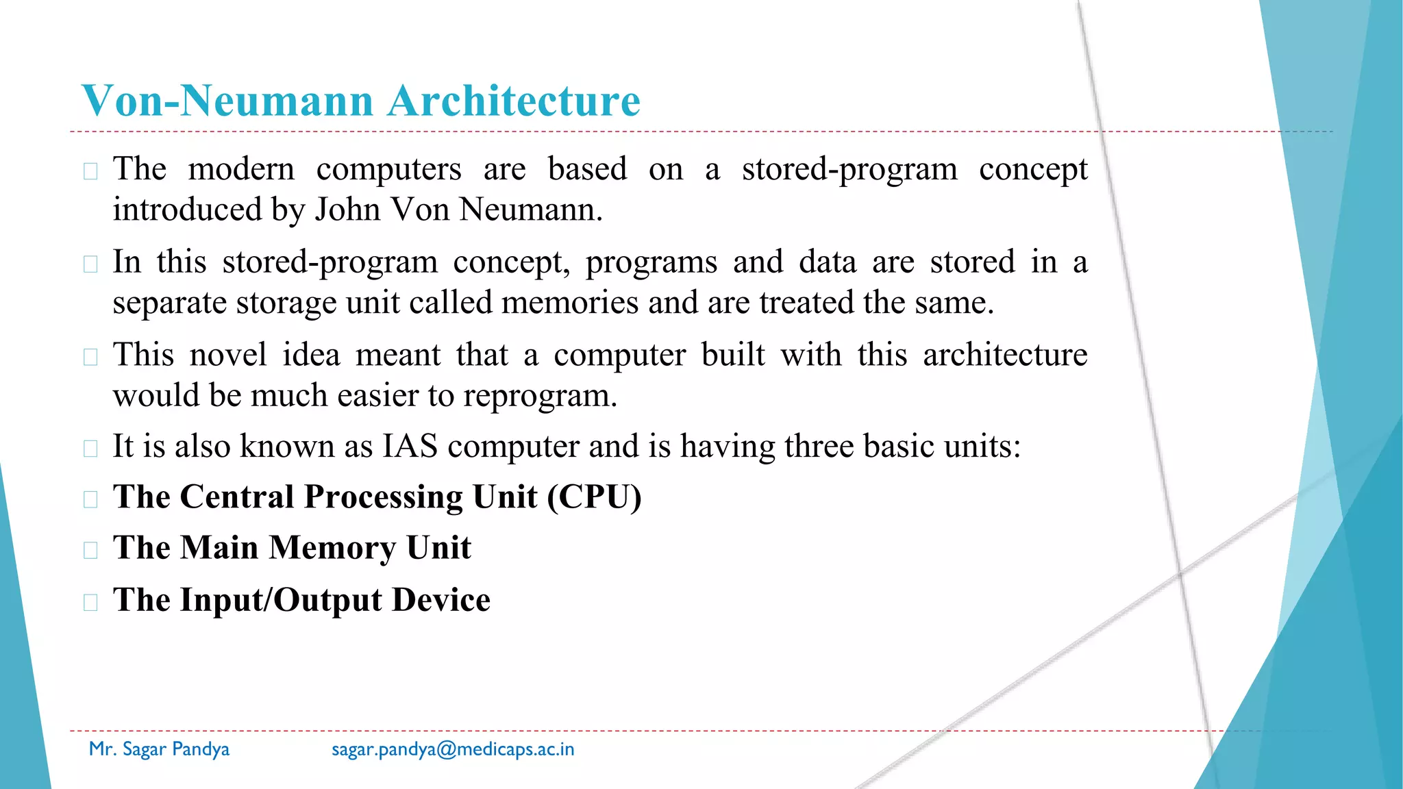
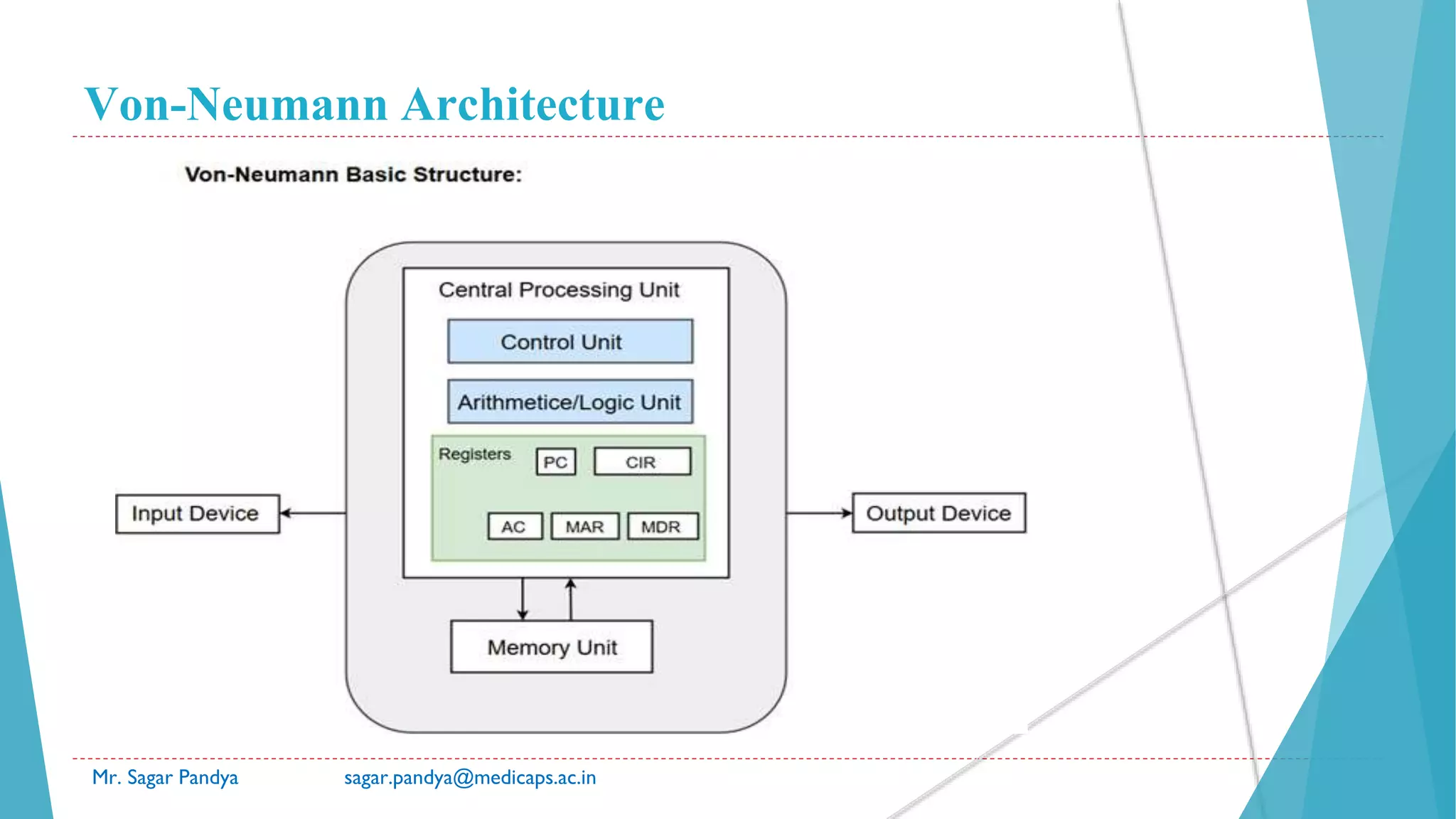
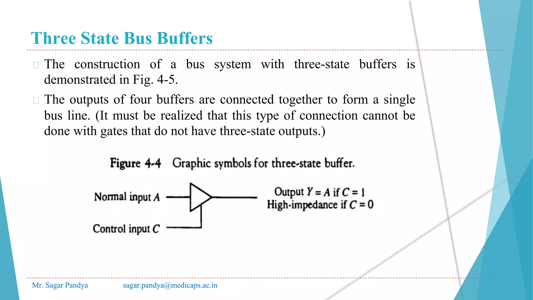
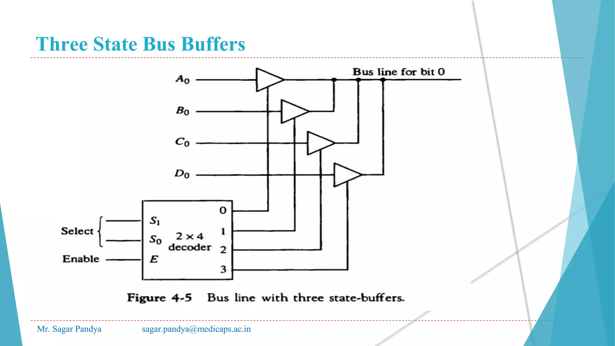
The document outlines the course structure for Computer System Architecture taught by Mr. Sagar Pandya at Medi-Caps University, detailing its content, references, and key concepts such as computer organization and architecture. It discusses the evolution of computers, the distinction between hardware and software, and outlines the basic architecture of computers, including the CPU, memory units, and I/O devices. Additionally, it covers the Von Neumann architecture and Flynn's classification of computers, emphasizing the importance of these concepts in computer design and functionality.
![INTRODUCTION
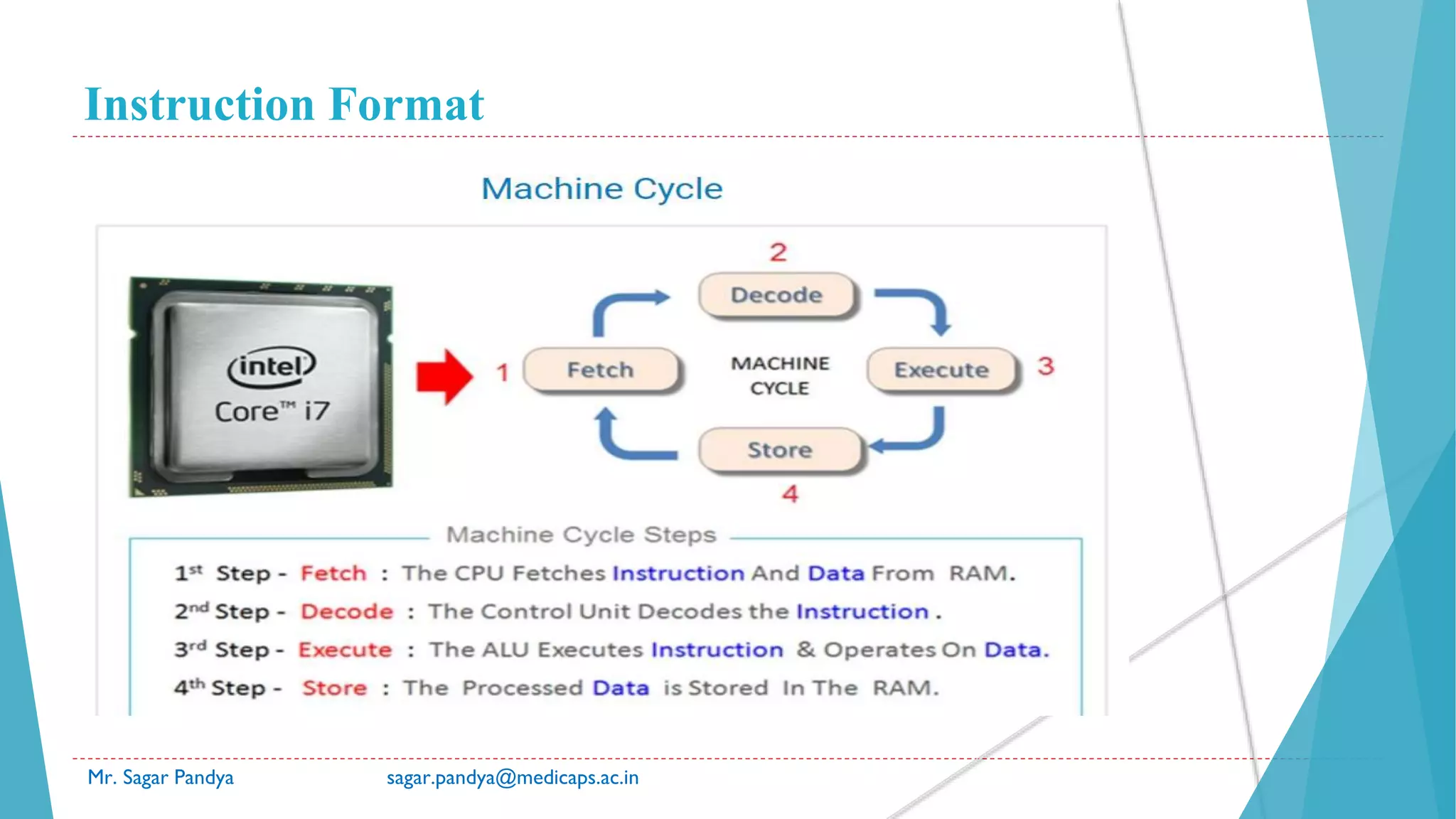
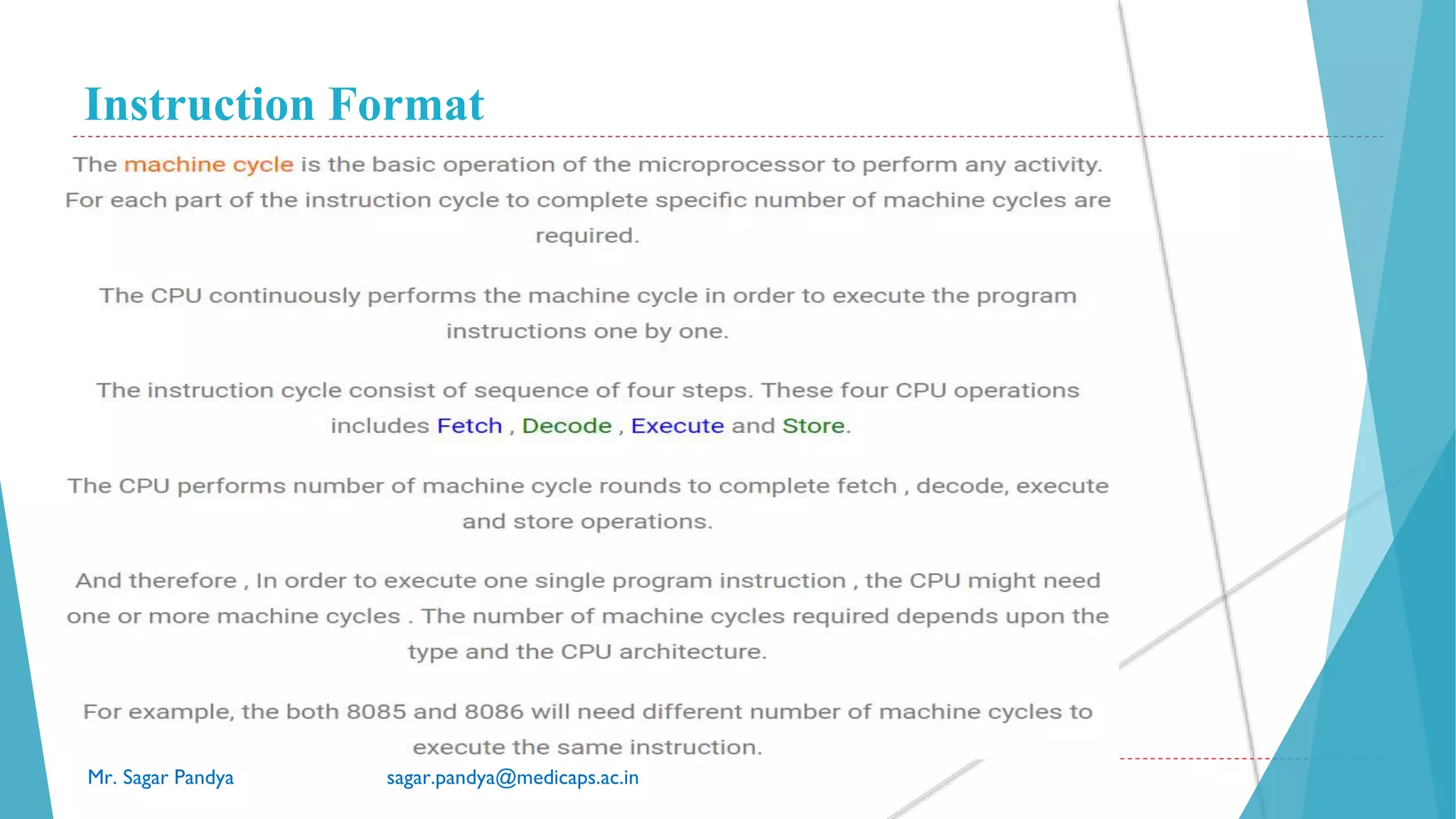
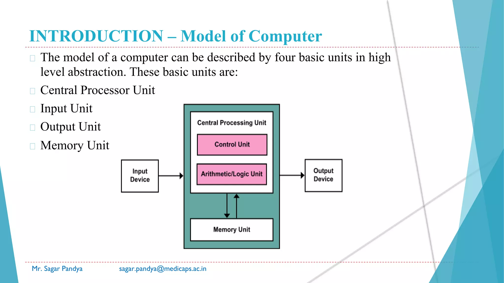
A. Central Processor Unit [CPU] :
� Central processor unit consists of two basic blocks :
� The program control unit has a set of registers and control circuit to
generate control signals.
� The execution unit or data processing unit contains a set of registers
for storing data and an Arithmetic and Logic Unit (ALU) for
execution of arithmetic and logical operations.
� In addition, CPU may have some additional registers for temporary
storage of data.
B. Input Unit :
� With the help of input unit data from outside can be supplied to the
computer.
Mr. Sagar Pandya sagar.pandya@medicaps.ac.in](https://image.slidesharecdn.com/unit-1csa-220413044102/75/UNIT-1-CSA-pptx-15-2048.jpg)


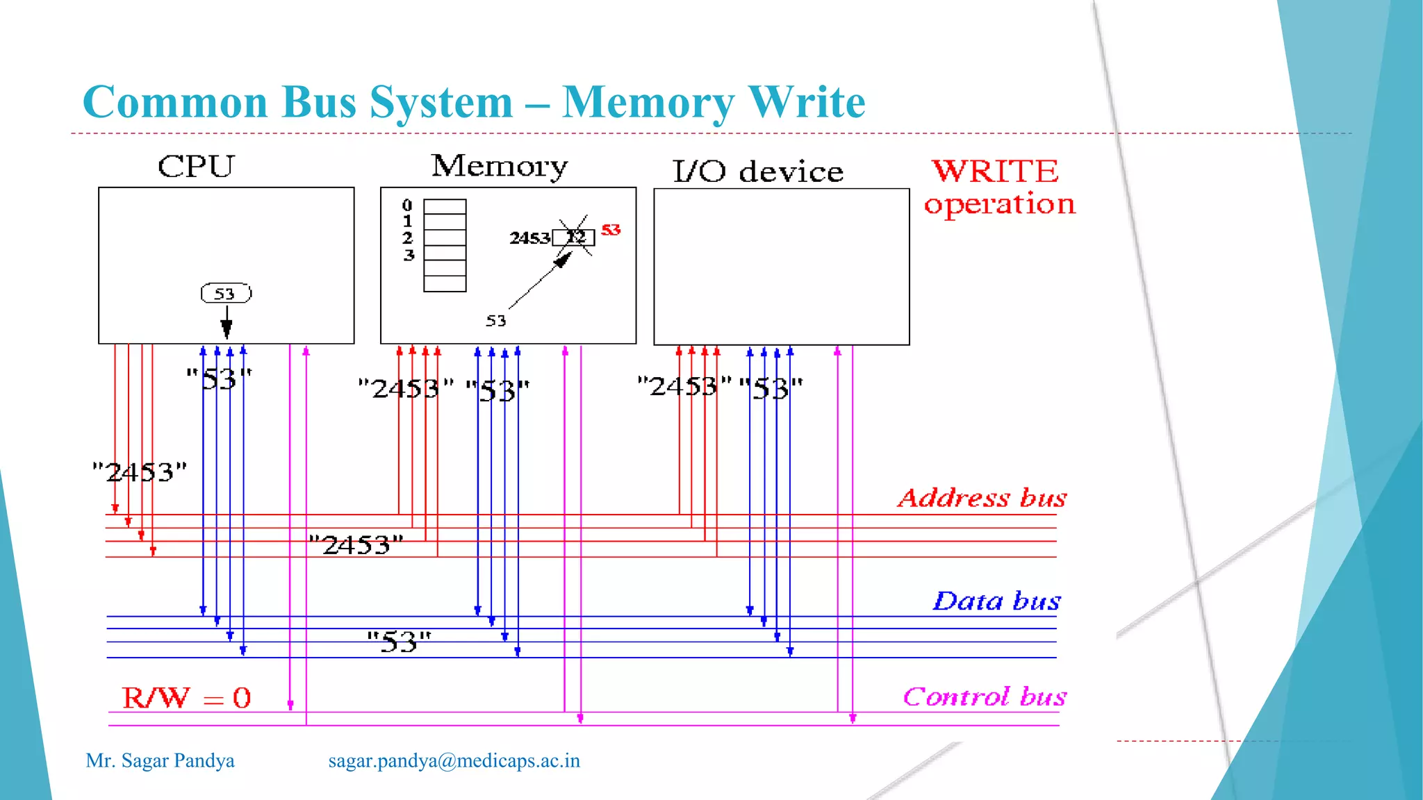
![Memory Transfer
Mr. Sagar Pandya sagar.pandya@medicaps.ac.in
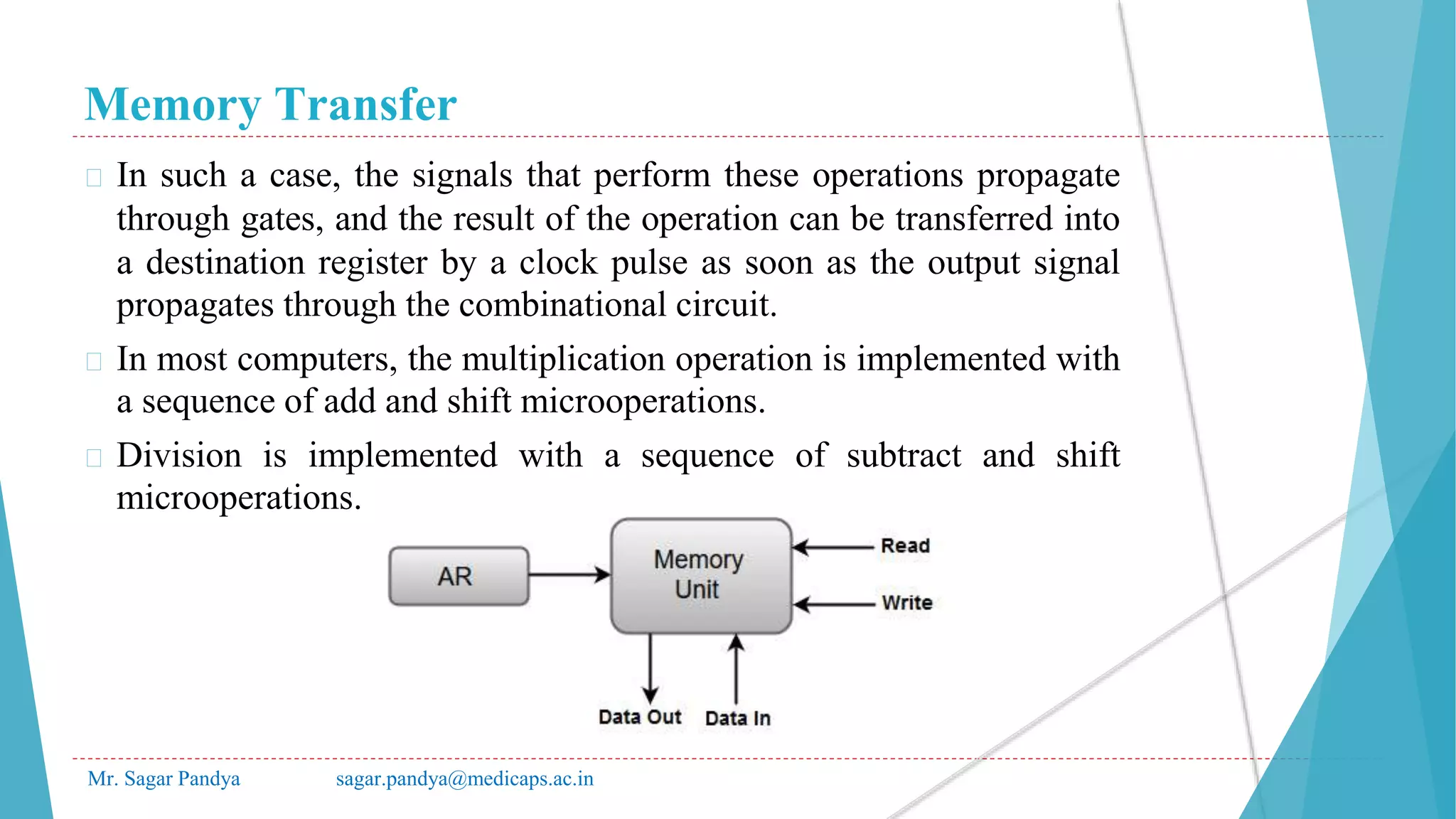
� The data are transferred to another register, called the data register,
symbolized by DR .
� The read operation can be stated as follows:
� Read: DR 🡨 M[AR]
� This causes a transfer of information into DR from the memory word
M selected by the address in AR .
� The write operation transfers the content of a data register to a
memory word M selected by the address.
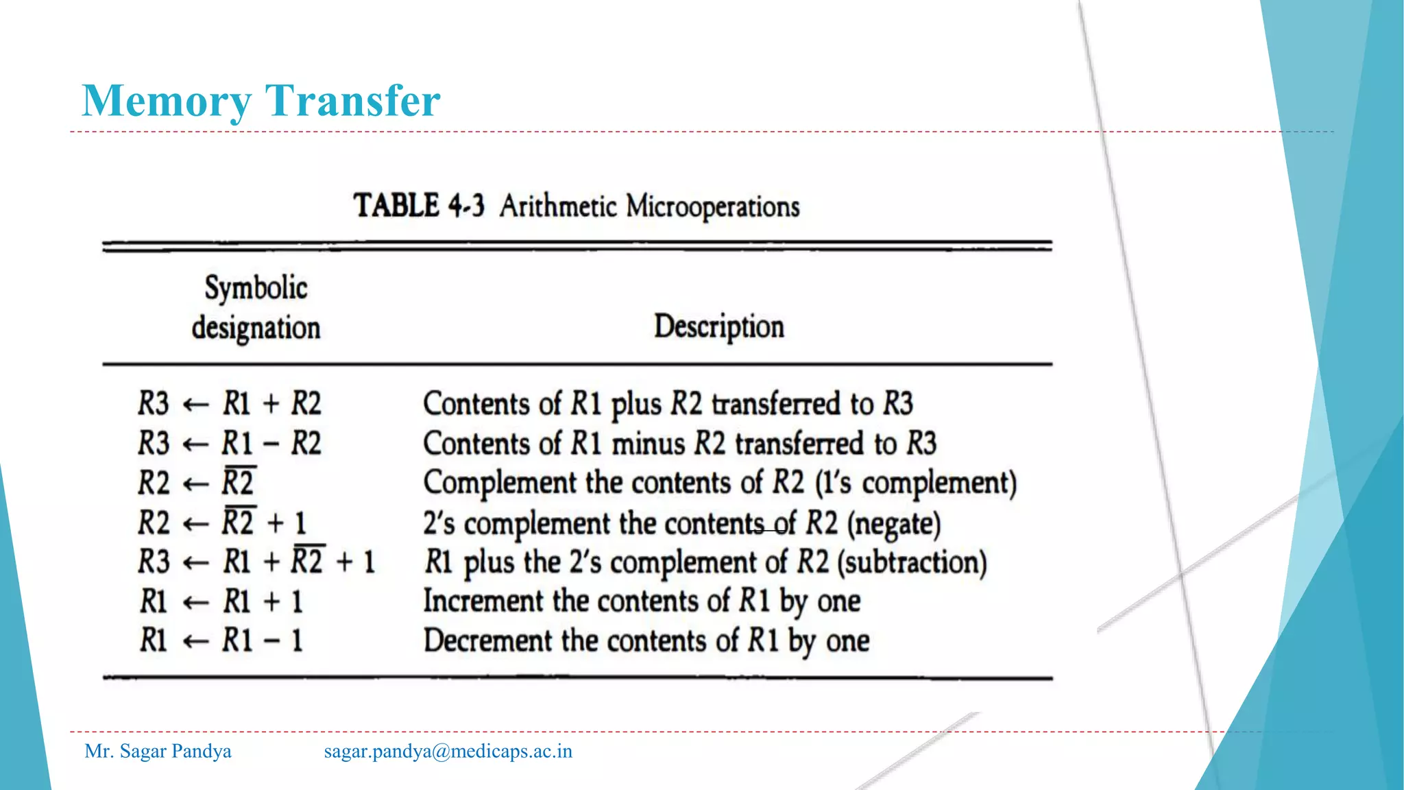
� Assume that the input data are in register Rl, R2 is the symbol for the
1' s complement of R2.
� Adding 1 to the 1's complement produces the 2's complement.
Adding the contents of R1 to the 2's complement of R2 is equivalent
to R1 - R2.](https://image.slidesharecdn.com/unit-1csa-220413044102/75/UNIT-1-CSA-pptx-82-2048.jpg)


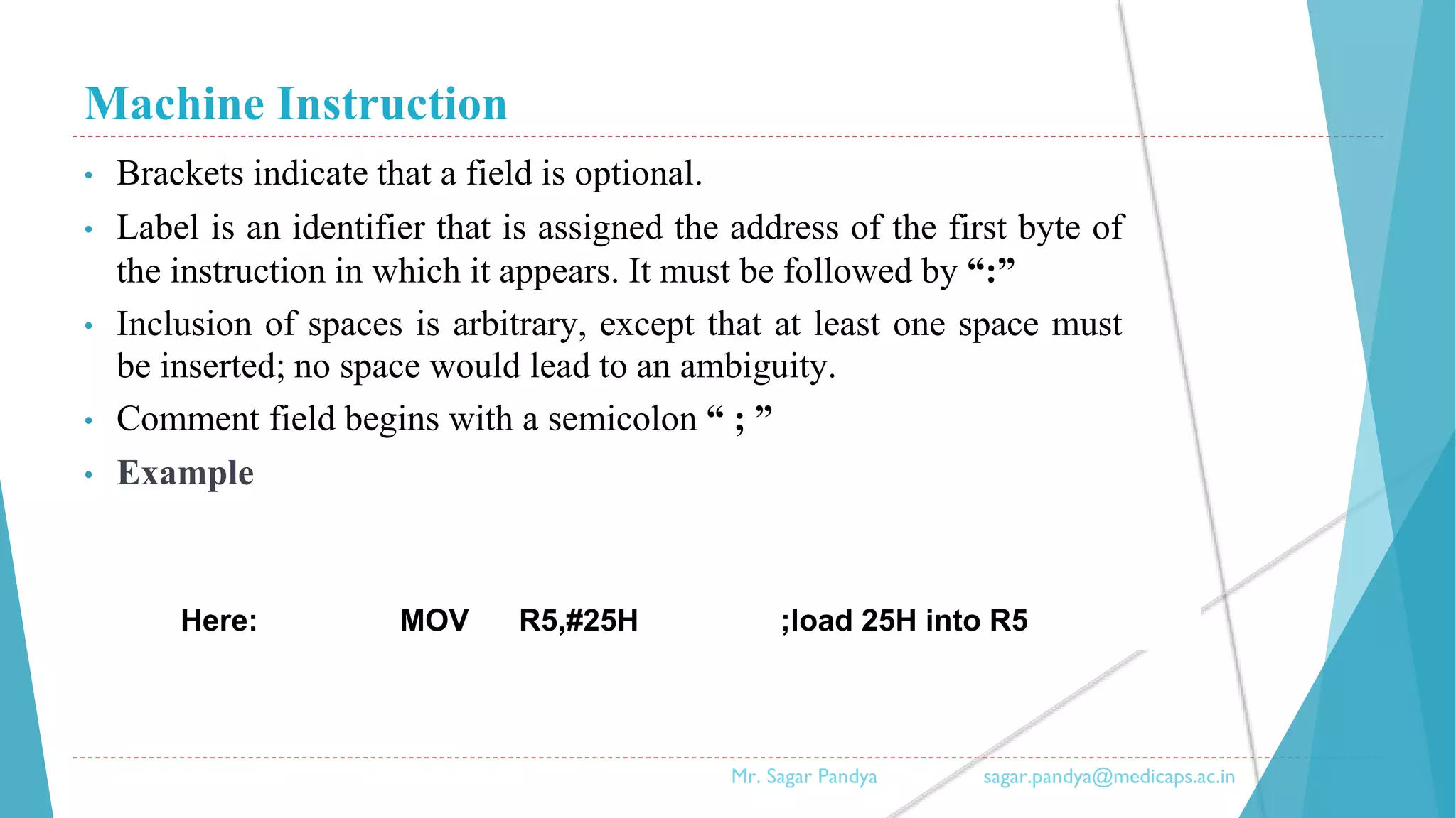
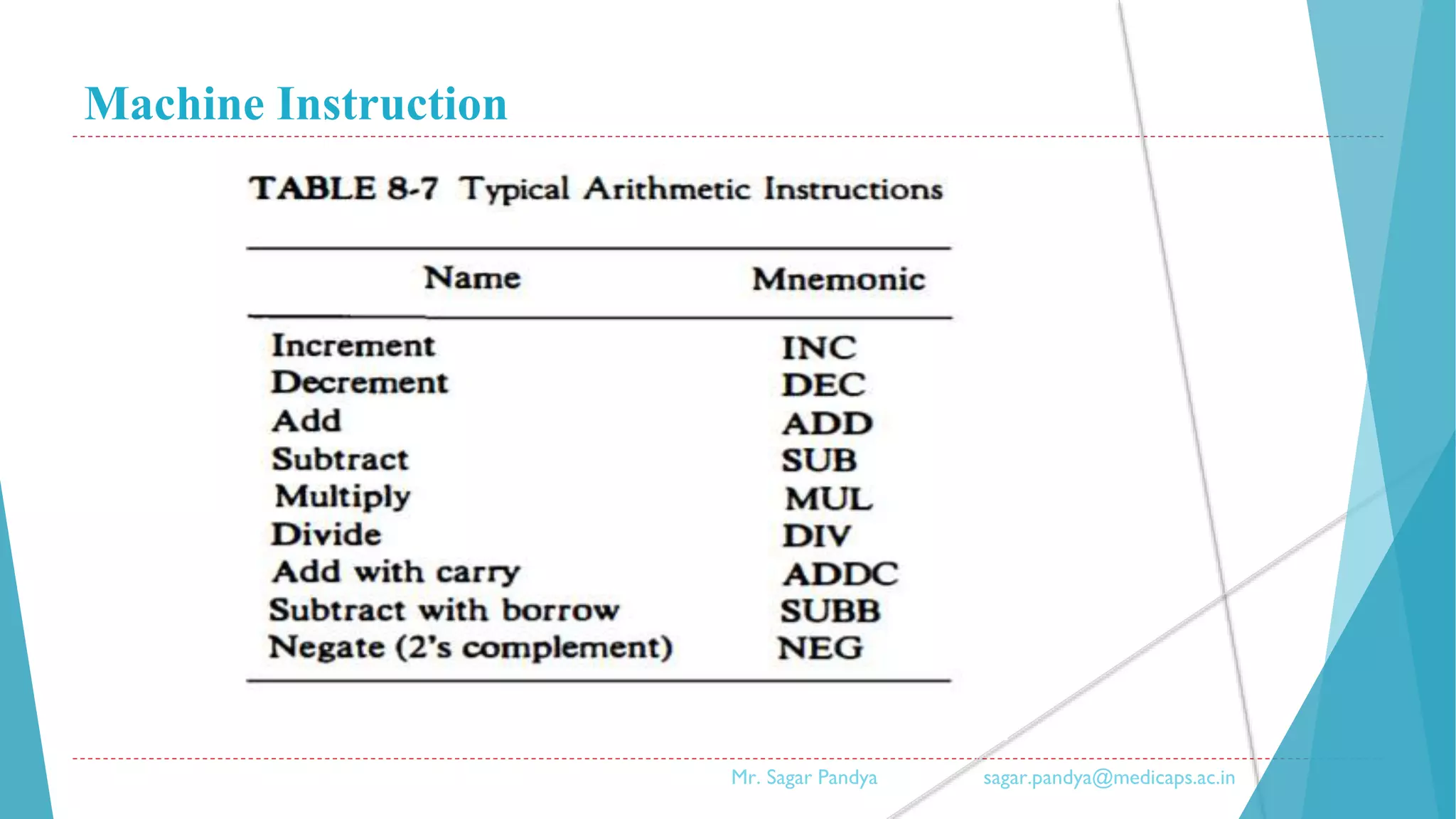
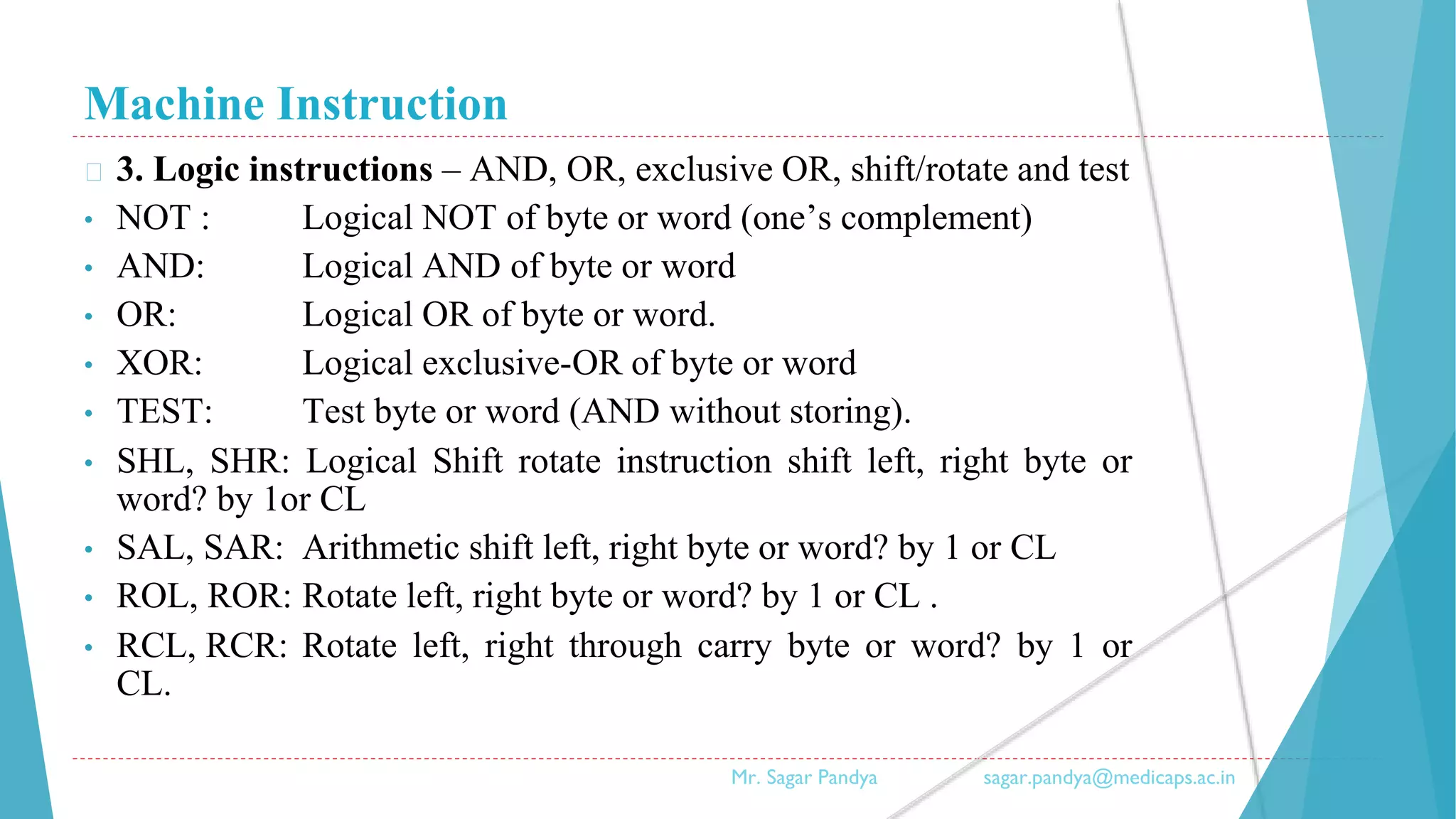
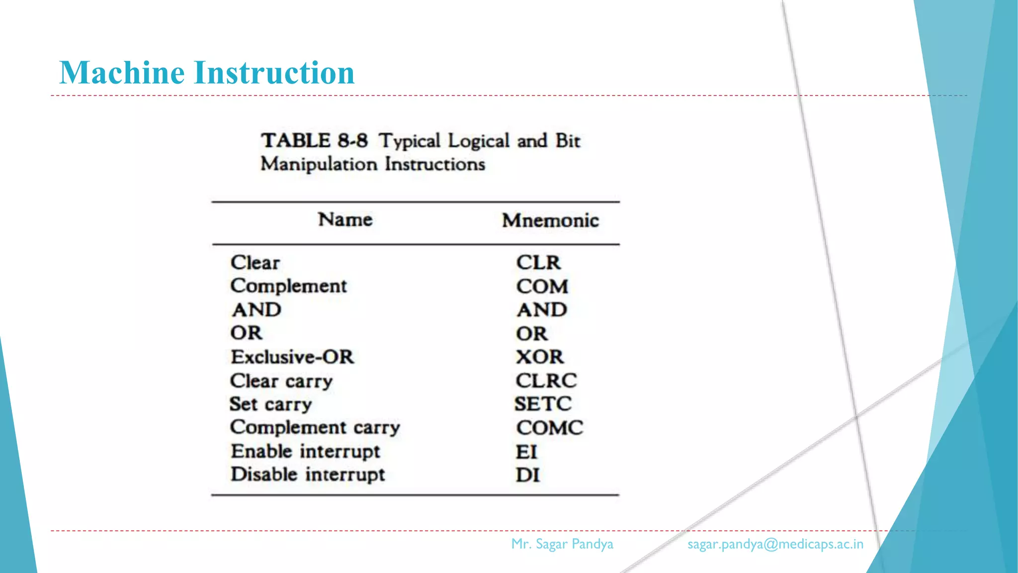
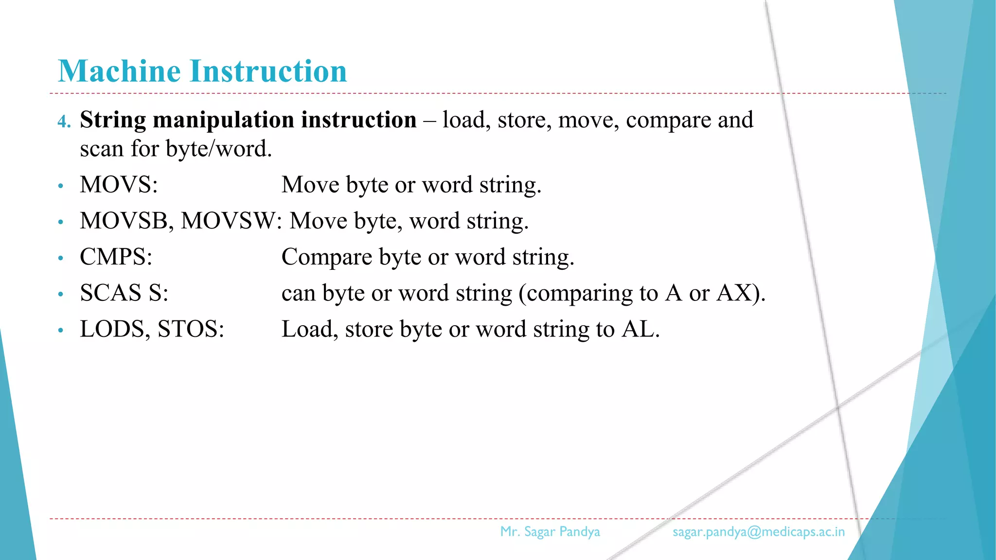
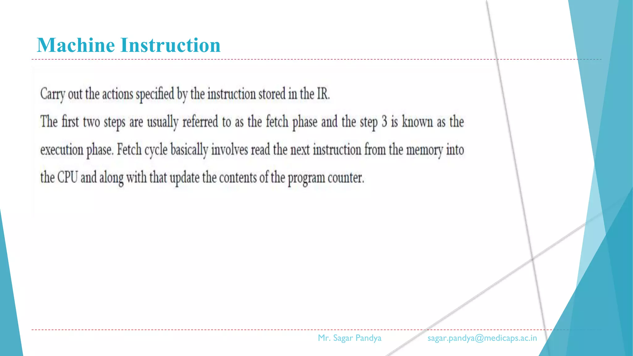
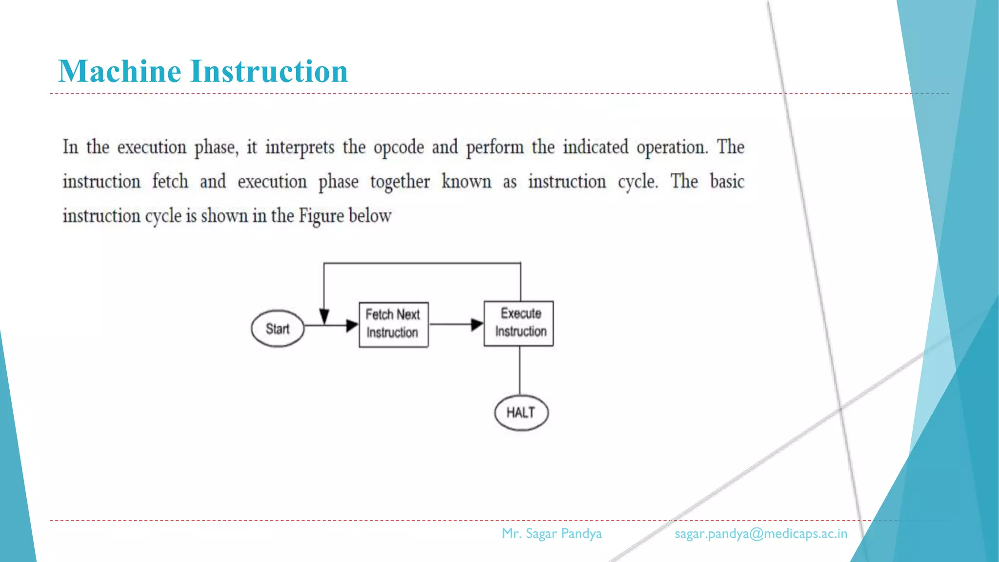
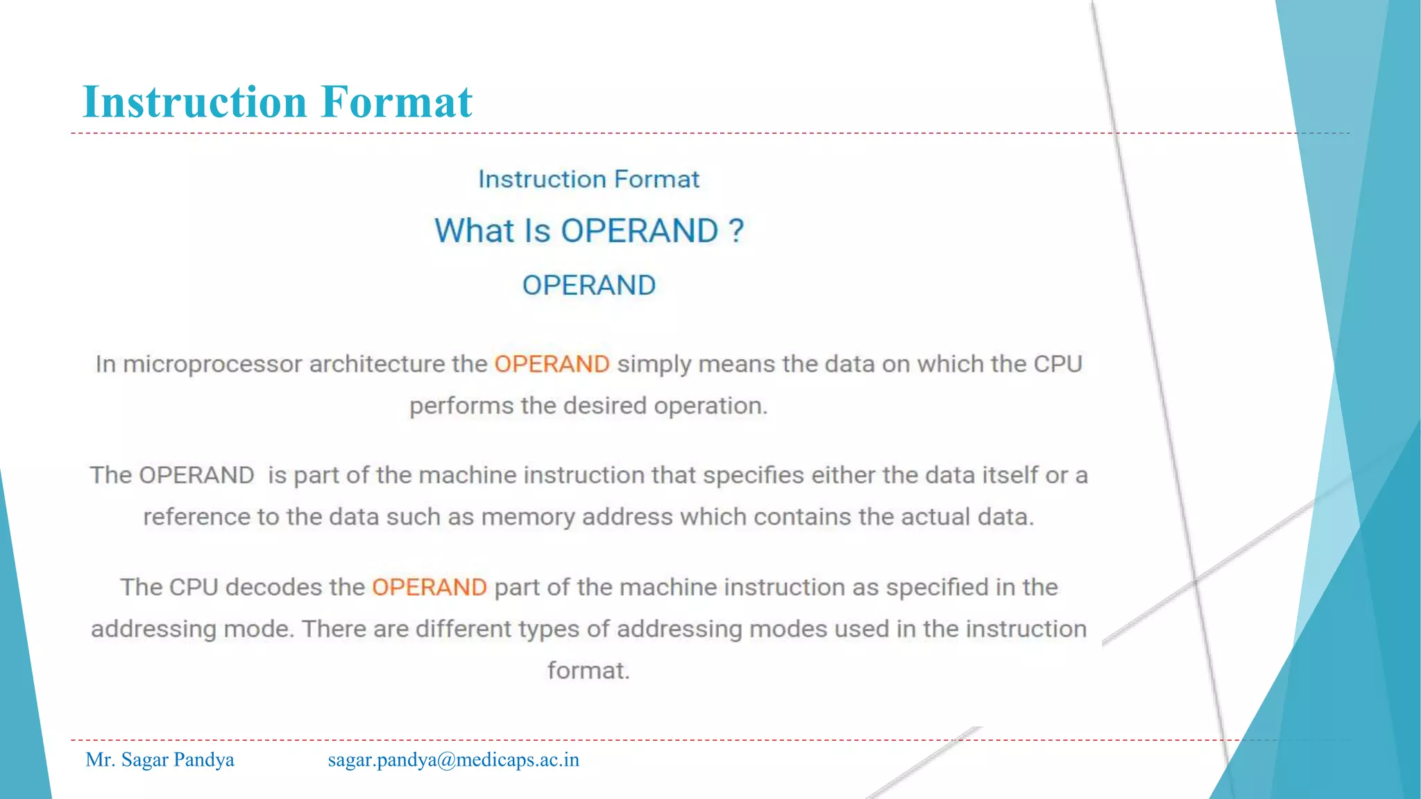
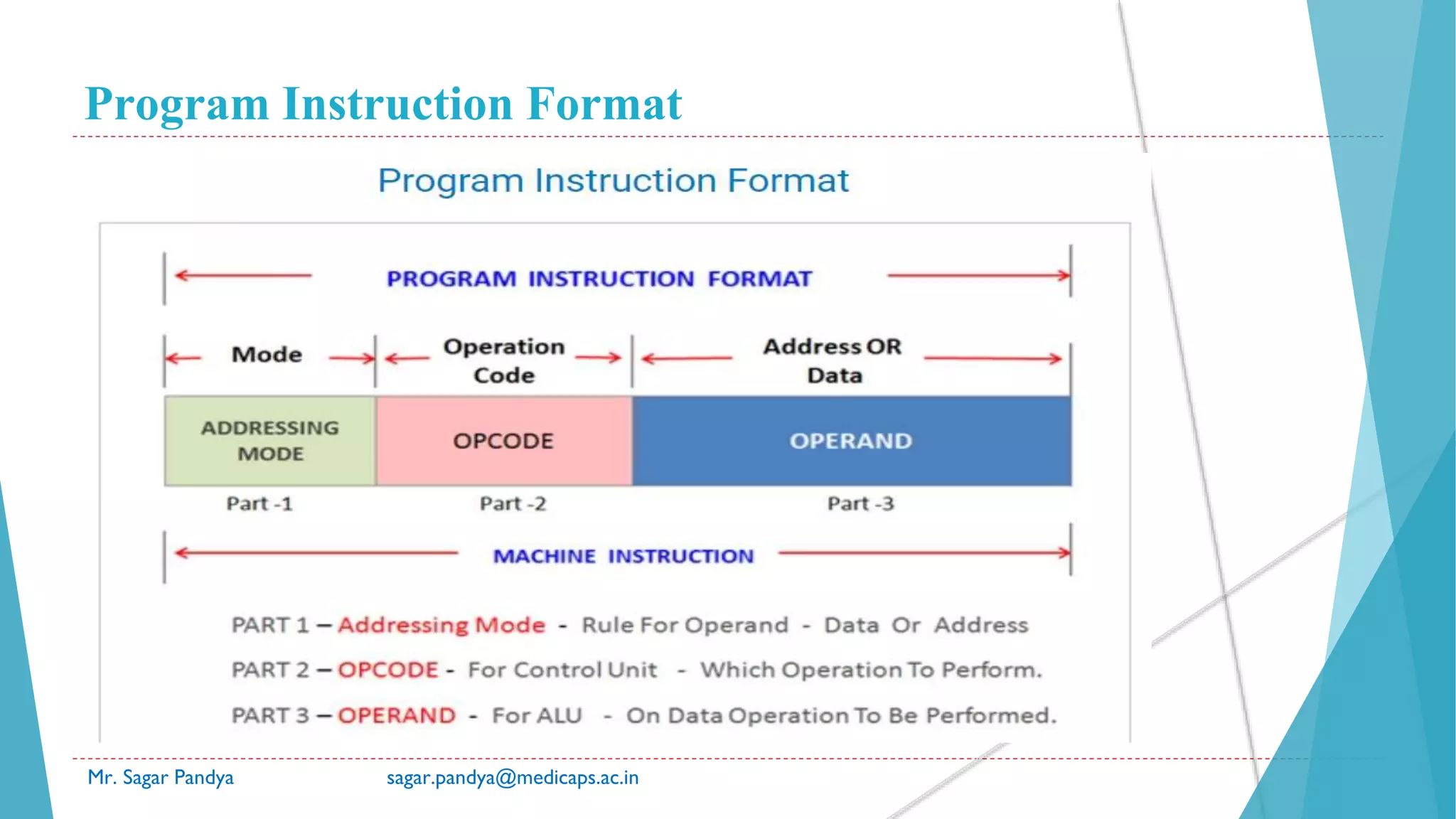
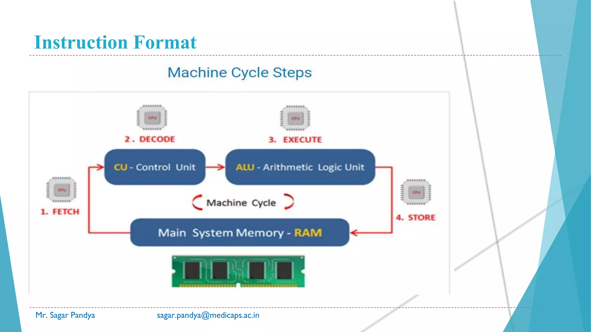
![Machine Instruction
� Machine code or machine language is a set of instructions executed
directly by a computer’s central processing unit (CPU).
� Each instruction performs a very specific task, such as a load, a
jump, or an ALU operation on a unit of data in a CPU register or
memory.
� Every program directly executed by a CPU is made up of a series of
such instructions.
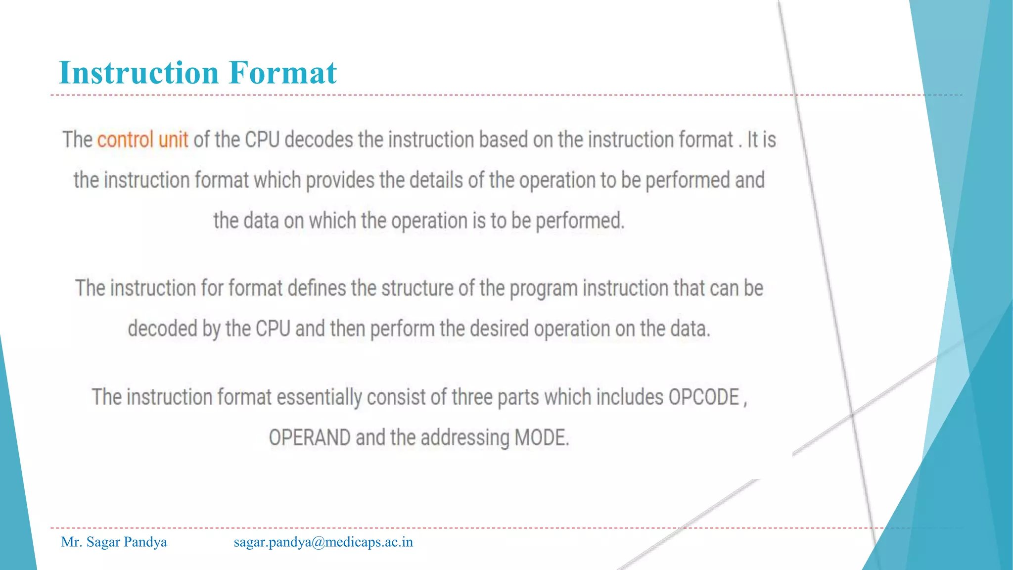
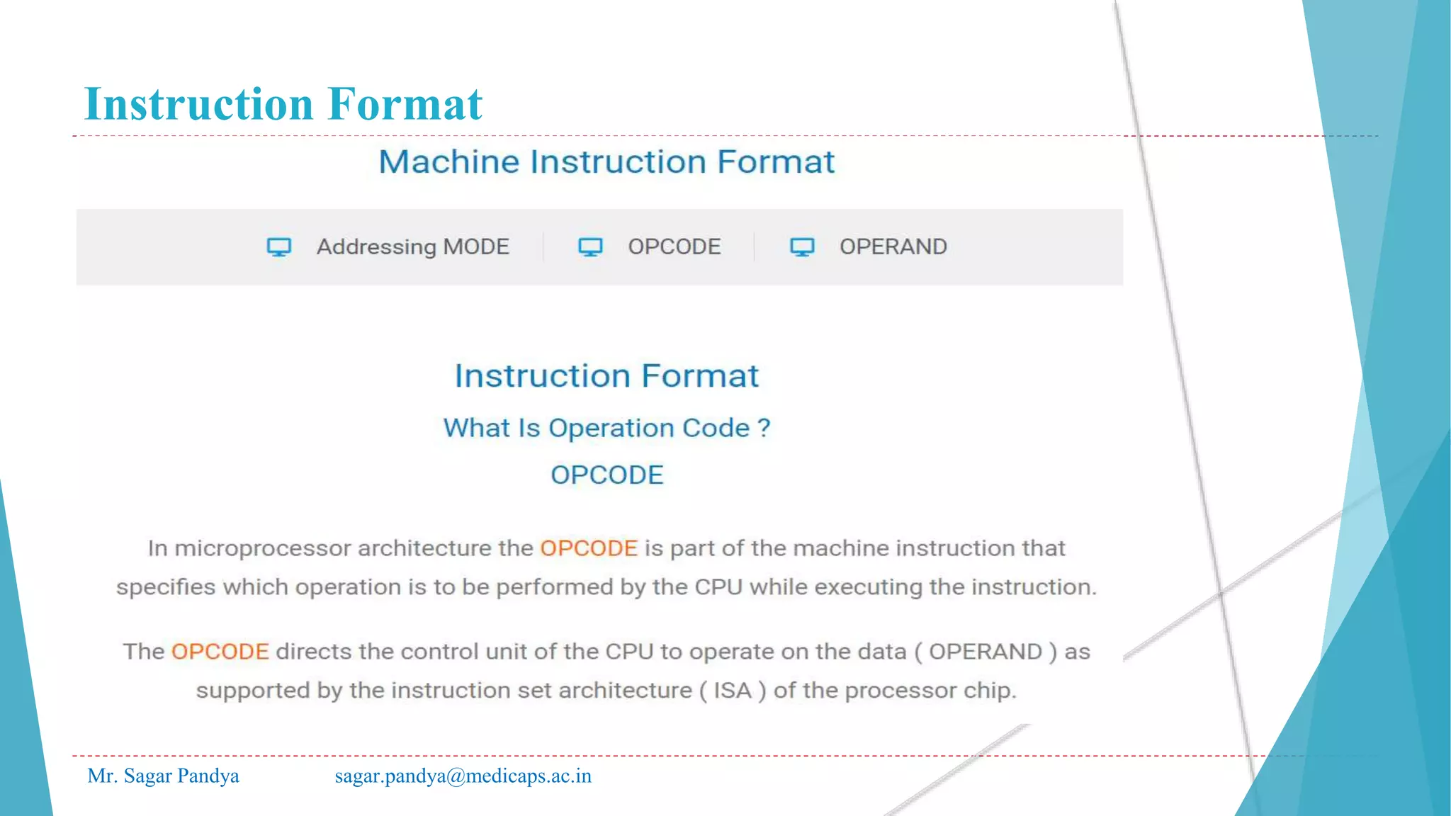
� The general format of a machine instruction is
Mr. Sagar Pandya sagar.pandya@medicaps.ac.in
[Label:] Mnemonic [Operand, Operand] [; Comments]](https://image.slidesharecdn.com/unit-1csa-220413044102/75/UNIT-1-CSA-pptx-113-2048.jpg)