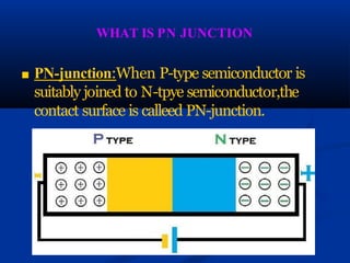
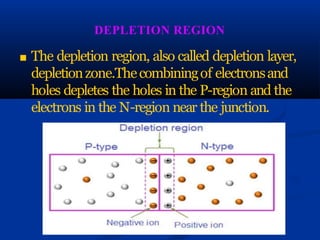
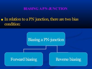
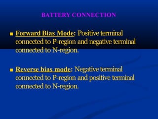
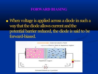
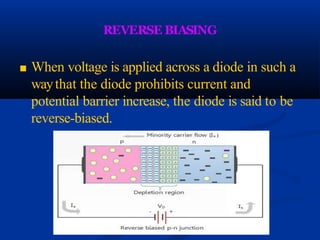
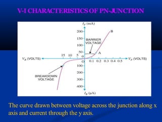
PN JUNCTION
BY-MEHEDI HASAN
SARIK
WHAT IS PN JUNCTION
■ PN-junction:When P-type semiconductor is
suitably joined to N-tpye semiconductor,the
contact surface is calleed PN-junction.
N-TYPE SEMICONDUCTOR
■ N-Type: Whenasmallamountof pentavalent
impurity is added to a pure semiconductor,it’s known
as a N-type semiconductor.
P-TYPE SEMICONDUCTOR
■ P-type:when a small amount of trivalent
impurity is added to a pure semiconductor,it’s
called P-type semiconductor.
DEPLETION REGION
■ The depletion region, also called depletion layer,
depletionzone.Thecombiningof electronsand
holes depletes the holes in the P-region and the
electrons in the N-region near the junction.
BIASING APN-JUNCTION
■ In relation to a PN junction, there are two bias
condition:
Biasing a PN-junction
Forward biasing Reverse biasing
BATTERY CONNECTION
■ Forward Bias Mode: Positiveterminal
connected to P-region and negative terminal
connected to N-region.
■ Reverse bias mode: Negativeterminal
connected to P-region and positive terminal
connected to N-region.
FORWARD BIASING
■ When voltage is applied across adiode in such a
waythatthediodeallowscurrentandthe
potential barrier reduced, the diode is said to be
forward-biased.
REVERSE BIASING
■ When voltage is applied across a diode in such a
waythat the diode prohibits current and
potential barrier increase, the diode is said to be
reverse-biased.
V-I CHARACTERISTICSOF PN-J
UNCTION
The curve drawn between voltage across the junction along x
axis and current through the y axis.
IN FORW
ARD BIAS
■ No current flows until the barrier voltage (0.3 for Ge) is
overcome.
■ Then the curve has linear rise and the current increase
with the increase forward voltage.
■ Above the 3v, the majority carriers passing the junction
gain sufficient energy to knock out the electrons.
■ Therefore, the forward current increase sharply.
IN REVERSE BIAS
■ Junction resistance, potential barrier increase.
■ When reverse voltage is increased beyond a
value, called breakdown voltage.
■ Reverse current increase sharply.
■ Above 25 reverse voltage, destroys the junction
permanently.
ADVANTAGE
■ No filament is necessary.
■ Occupies lesser space.
■ Long life.
THANKSEVERYBODY

pn-junction-151216100718 (1).pptx

  • 1.
  • 2.
    WHAT IS PNJUNCTION ■ PN-junction:When P-type semiconductor is suitably joined to N-tpye semiconductor,the contact surface is calleed PN-junction.
  • 3.
    N-TYPE SEMICONDUCTOR ■ N-Type:Whenasmallamountof pentavalent impurity is added to a pure semiconductor,it’s known as a N-type semiconductor.
  • 4.
    P-TYPE SEMICONDUCTOR ■ P-type:whena small amount of trivalent impurity is added to a pure semiconductor,it’s called P-type semiconductor.
  • 5.
    DEPLETION REGION ■ Thedepletion region, also called depletion layer, depletionzone.Thecombiningof electronsand holes depletes the holes in the P-region and the electrons in the N-region near the junction.
  • 6.
    BIASING APN-JUNCTION ■ Inrelation to a PN junction, there are two bias condition: Biasing a PN-junction Forward biasing Reverse biasing
  • 7.
    BATTERY CONNECTION ■ ForwardBias Mode: Positiveterminal connected to P-region and negative terminal connected to N-region. ■ Reverse bias mode: Negativeterminal connected to P-region and positive terminal connected to N-region.
  • 8.
    FORWARD BIASING ■ Whenvoltage is applied across adiode in such a waythatthediodeallowscurrentandthe potential barrier reduced, the diode is said to be forward-biased.
  • 9.
    REVERSE BIASING ■ Whenvoltage is applied across a diode in such a waythat the diode prohibits current and potential barrier increase, the diode is said to be reverse-biased.
  • 10.
    V-I CHARACTERISTICSOF PN-J UNCTION Thecurve drawn between voltage across the junction along x axis and current through the y axis.
  • 11.
    IN FORW ARD BIAS ■No current flows until the barrier voltage (0.3 for Ge) is overcome. ■ Then the curve has linear rise and the current increase with the increase forward voltage. ■ Above the 3v, the majority carriers passing the junction gain sufficient energy to knock out the electrons. ■ Therefore, the forward current increase sharply.
  • 12.
    IN REVERSE BIAS ■Junction resistance, potential barrier increase. ■ When reverse voltage is increased beyond a value, called breakdown voltage. ■ Reverse current increase sharply. ■ Above 25 reverse voltage, destroys the junction permanently.
  • 13.
    ADVANTAGE ■ No filamentis necessary. ■ Occupies lesser space. ■ Long life.
  • 14.