Download to read offline

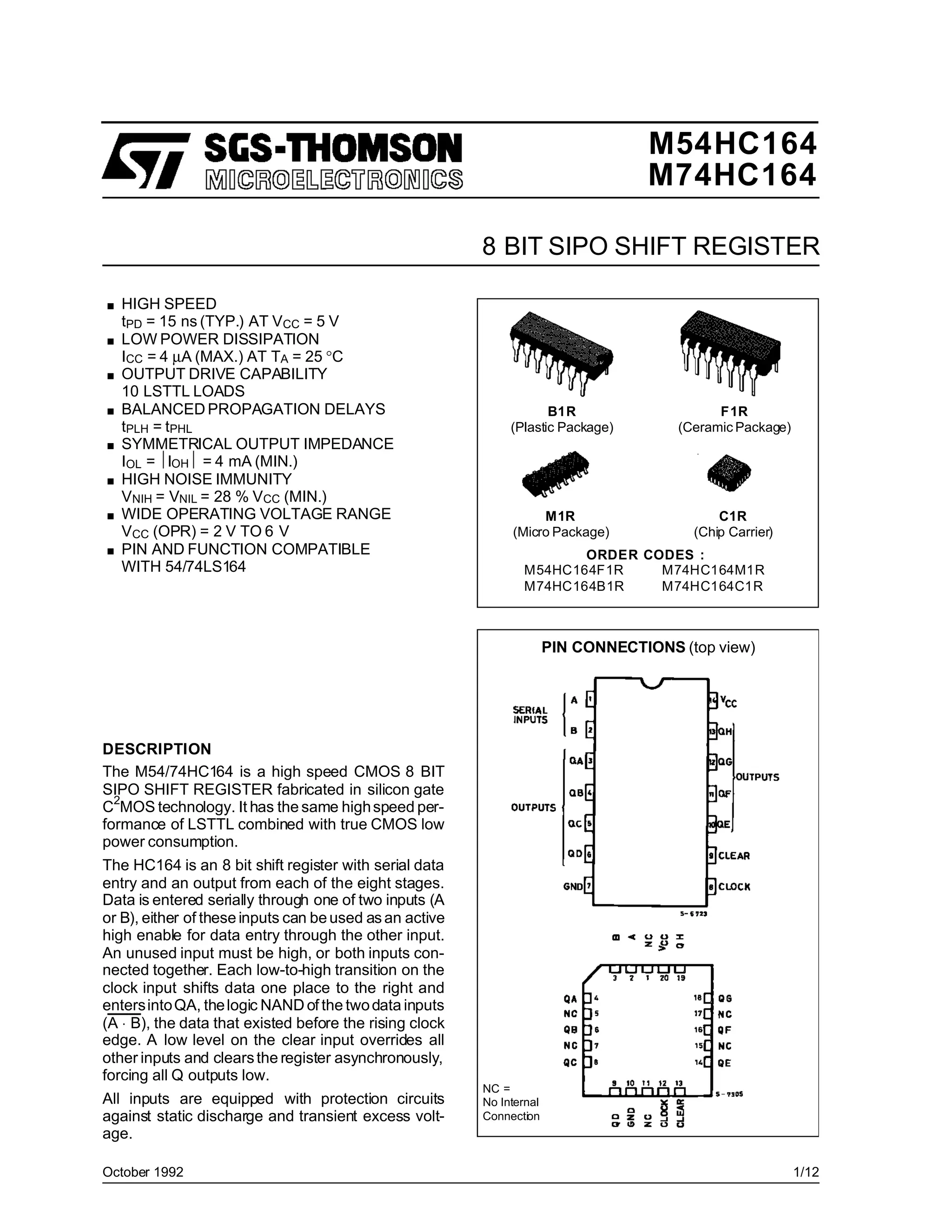

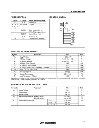

This document describes an 8-bit shift register chip. It provides high-speed performance with low power consumption. The chip allows serial data entry through two inputs and outputs one bit per stage. It can be cleared asynchronously. The document includes pin descriptions, logic diagrams, timing diagrams, and specifications for electrical characteristics and packaging.