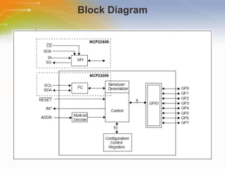
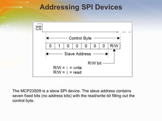
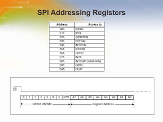
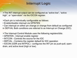
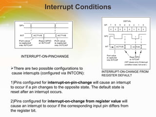
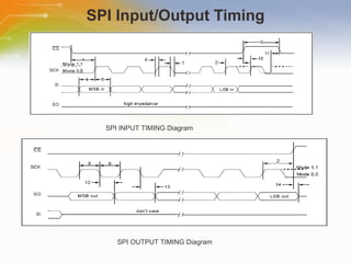
Study On MCP23S09 I/O Expander with SPI Interface Source: Microchip Technology Inc
Introduction Purpose To Learn the working and operation of the MCP23S09 SPI Interfaced I/O Expander Device. Outline Features Block Diagram Serial Interface / SPI Addressing Interrupt Logic and Conditions SPI Input output Timings Content 12 pages
Features 8-bit   remote   bidirectional   I/O   port:   I/O   pins   default   to   input   Open-drain   outputs:   5.5V   tolerant. 25   mA   sink.   200   mA   total.   High-speed   I2C™   interface:   ( MCP23009 ) -   100   kHz,   400   kHz,   3.4MHz. Low   standby   current   as   low   as   1   μA. High-speed   SPI   interface   at   10   MHz   ( MCP23S09) Configurable   interrupt   output   pins:   Configurable   as   active-high,   active-low   or   open-drain. Configurable   interrupt   source:   Interrupt-on-change   from   configured   defaults   or   pin   change. Single   hardware   address   pin:   (MCP23009) -   Voltage   input   to   allow   up   to   eight   devices   on   the   bus Polarity   inversion   register   to   configure   the   polarity   of   the   input   port   data. External   reset   input.
Block Diagram
Serial Interface This   block   handles   the   functionality   of   the   I2C   (MCP23009)   or   SPI   (MCP23S09)   interface   protocol. The   MCP23X09   contains   eleven   individual   registers   which   can   be   addressed   through   the   Serial   Interface   block. The   MCP23X09   has   the   ability   to   operate   in   “Byte   Mode”   or   “Sequential   Mode”. Byte   Mode   disables   automatic   address   pointer   incrementing.   This   Mode   gives   the   ability   to   continually   access   the   same   address   by   providing   extra   clocks. Sequential   Mode   enables   automatic   address   pointer   incrementing.   The   MCP23X09   increments   its   address   counter   after   each byte   during   the   data   transfer.   The   address   pointer   automatically   rolls   over   to   address   00h   after   accessing   the   last   register.
Addressing SPI Devices The MCP23S09 is a slave SPI device. The slave address contains seven fixed bits (no address bits) with the read/write bit filling out the control byte.
SPI Addressing Registers
Interrupt Logic The INT interrupt output can be configured as “active low”, “active high”, or “open-drain” via the IOCON register. Each pin is individually configurable as follows: •  Enable/disable interrupt via GPINTEN •  Can interrupt on either pin change or change from default as configured in DEFVAL Both conditions are referred to as Interrupt on Change (IOC). The Interrupt Control Module uses the following registers/bits: •  GPINTEN - Interrupt enable register •  INTCON - Controls the source for the IOC •  DEFVAL - Contains the register default for IOC operation •  IOCON (ODR and INTPOL) - configures the INT pin as push-pull, open-drain, and active level (high or low).
Interrupt Conditions INTERRUPT-ON-PINCHANGE INTERRUPT-ON-CHANGE FROM  REGISTER DEFAULT There are two possible configurations to cause interrupts (configured via INTCON): 1)Pins configured for  interrupt-on-pin-change  will cause an interrupt to occur if a pin changes to the opposite state. The default state is reset after an interrupt occurs. 2)Pins configured for  interrupt-on-change from register value  will cause an interrupt to occur if the corresponding input pin differs from the register bit.
SPI Input/Output Timing SPI INPUT TIMING Diagram SPI OUTPUT TIMING Diagram
Typical Performance Curve For SPI Tv Specification
Additional Resource For ordering the MCP23S09, please click the part list or Call our sales hotline For additional inquires contact our technical service hotline For more product information go to  http://www.microchip.com/wwwproducts/Devices.aspx?dDocName=en538921 Newark Farnell

Study On MCP23S09 I/O Expander with SPI Interface

  • 1.
    Study On MCP23S09I/O Expander with SPI Interface Source: Microchip Technology Inc
  • 2.
    Introduction Purpose ToLearn the working and operation of the MCP23S09 SPI Interfaced I/O Expander Device. Outline Features Block Diagram Serial Interface / SPI Addressing Interrupt Logic and Conditions SPI Input output Timings Content 12 pages
  • 3.
    Features 8-bit remote bidirectional I/O port: I/O pins default to input Open-drain outputs: 5.5V tolerant. 25 mA sink. 200 mA total. High-speed I2C™ interface: ( MCP23009 ) - 100 kHz, 400 kHz, 3.4MHz. Low standby current as low as 1 μA. High-speed SPI interface at 10 MHz ( MCP23S09) Configurable interrupt output pins: Configurable as active-high, active-low or open-drain. Configurable interrupt source: Interrupt-on-change from configured defaults or pin change. Single hardware address pin: (MCP23009) - Voltage input to allow up to eight devices on the bus Polarity inversion register to configure the polarity of the input port data. External reset input.
  • 4.
  • 5.
    Serial Interface This block handles the functionality of the I2C (MCP23009) or SPI (MCP23S09) interface protocol. The MCP23X09 contains eleven individual registers which can be addressed through the Serial Interface block. The MCP23X09 has the ability to operate in “Byte Mode” or “Sequential Mode”. Byte Mode disables automatic address pointer incrementing. This Mode gives the ability to continually access the same address by providing extra clocks. Sequential Mode enables automatic address pointer incrementing. The MCP23X09 increments its address counter after each byte during the data transfer. The address pointer automatically rolls over to address 00h after accessing the last register.
  • 6.
    Addressing SPI DevicesThe MCP23S09 is a slave SPI device. The slave address contains seven fixed bits (no address bits) with the read/write bit filling out the control byte.
  • 7.
  • 8.
    Interrupt Logic TheINT interrupt output can be configured as “active low”, “active high”, or “open-drain” via the IOCON register. Each pin is individually configurable as follows: • Enable/disable interrupt via GPINTEN • Can interrupt on either pin change or change from default as configured in DEFVAL Both conditions are referred to as Interrupt on Change (IOC). The Interrupt Control Module uses the following registers/bits: • GPINTEN - Interrupt enable register • INTCON - Controls the source for the IOC • DEFVAL - Contains the register default for IOC operation • IOCON (ODR and INTPOL) - configures the INT pin as push-pull, open-drain, and active level (high or low).
  • 9.
    Interrupt Conditions INTERRUPT-ON-PINCHANGEINTERRUPT-ON-CHANGE FROM REGISTER DEFAULT There are two possible configurations to cause interrupts (configured via INTCON): 1)Pins configured for interrupt-on-pin-change will cause an interrupt to occur if a pin changes to the opposite state. The default state is reset after an interrupt occurs. 2)Pins configured for interrupt-on-change from register value will cause an interrupt to occur if the corresponding input pin differs from the register bit.
  • 10.
    SPI Input/Output TimingSPI INPUT TIMING Diagram SPI OUTPUT TIMING Diagram
  • 11.
    Typical Performance CurveFor SPI Tv Specification
  • 12.
    Additional Resource Forordering the MCP23S09, please click the part list or Call our sales hotline For additional inquires contact our technical service hotline For more product information go to http://www.microchip.com/wwwproducts/Devices.aspx?dDocName=en538921 Newark Farnell

Editor's Notes

  • #3 Welcome to the training module on MCP23S09 - an 8-bit, general purpose parallel I/O expansion for I2C bus or SPI applications with Open-Drain Outputs.
  • #4 The MCP23S09 is an 8-bit I/O expander with SPI interface operating at 10 MHz. It’s i/o can act as hardware interrupt, with 25 mA source/sink current per I/O. The MCP23X09 consists of multiple 8-bit configuration registers for input, output and polarity selection. The system master can enable the I/Os as either inputs or outputs by writing the I/O configuration bits. The data for each input or output is kept in the corresponding input or output register. The polarity of the input port register can be inverted with the polarity inversion register. All registers can be read by the system master.
  • #5 There are two versions of this device. • The MCP23009 – which has an I2C interface and the • MCP23S09 - SPI interface When any input state differs from its corresponding input port register state. This is used to indicate to the system master that an input state has changed. When an input state differs from a preconfigured register value (DEFVAL register). The Interrupt Capture register captures port values at the time of the interrupt, thereby saving the condition that caused the interrupt. The Power-on Reset (POR) sets the registers to their default values and initializes the device state machine. The hardware address pin is used to determine the device address.
  • #6 Here we show SPI interface block which the MCP23s09 implements. It has 11 individual registers which can be adressed through serial interface block. And it can also operate in 2 modes: Byte Mode and Sequential Mode: Byte Mode, stops the automatic address pointer from being inscreaded. Sequential modes enables automatic address pointer increase.
  • #7 In this diagram, we show how SPI Devices are addressed. It has 8-bits which is a control Byte out of which the first 7-bits represents slave address and the 8 th bit represents whether it is Read or Write operation to be performed to the slave Address it represents.
  • #8 This slide shows the SPI Addressing Registers and the timing format while addressing the register.
  • #9 This slides addresses how Interrupt Logic is configured in MCP23S09. The INT interrupt output can be configured as “active low”, “active high”, or “open-drain” via the IOCON register. Each pin is controlled through GPINTEN (Enable/Disable).
  • #10 Only those pins that are configured as an input (IODIR register) with interrupt-on-change (IOC) enabled (GPINTEN register) can cause an interrupt. Pins configured as an output have no effect on the interrupt output pin. Input change activity on a port input pin that is enabled for IOC will generate an internal device interrupt and the device will capture the value of the port and copy it into INTCAP. The first interrupt event will cause the port contents to be copied into the INTCAP register. Subsequent interrupt conditions on the port will not cause an interrupt to occur as long as the interrupt is not cleared by a read of INTCAP or GPIO. The interrupt will remain active until the INTCAP or GPIO register is read. The interrupt condition will be cleared after the LSb of the data is clocked out during a Read operation of GPIO or INTCAP.
  • #11 This slide shows SPI Input and Output Timing diagram.
  • #12 Here we show a Typical Performance Curve for Output Valid from Clock Low Tv verses Vdd.
  • #13 Thank you for taking the time to view this presentation on MCP23S09 . If you would like to learn more or go on to purchase some of these devices, you may either click on the part list link, or simple call our sales hotline. For more technical information you may either visit the Microchip Technology Inc site or if you would prefer to speak to someone live, please call our hotline number, or even use our ‘live chat’ online facility.