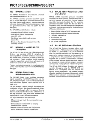
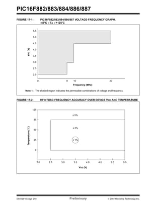
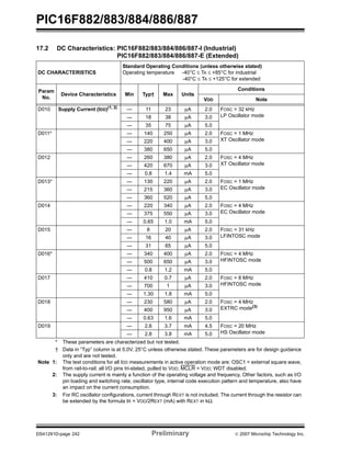
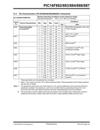
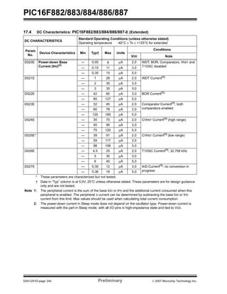
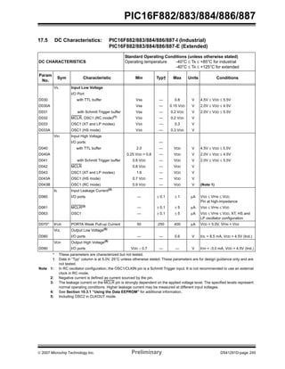
The document discusses code protection features for Microchip devices. It notes that Microchip products meet specifications in their data sheets. While code protection is designed to secure devices, there are possible illegal methods to breach it by operating outside specifications. Microchip works with customers concerned about code integrity and is committed to improving security, but cannot guarantee that code cannot be accessed, as security is constantly evolving.


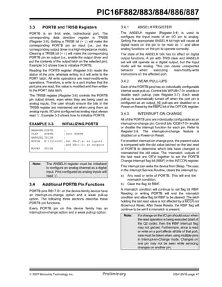
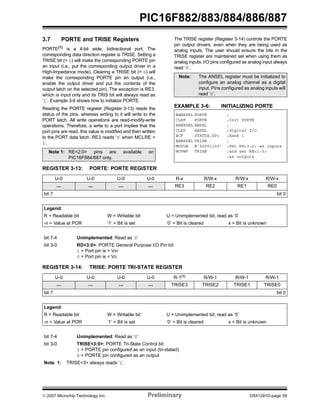

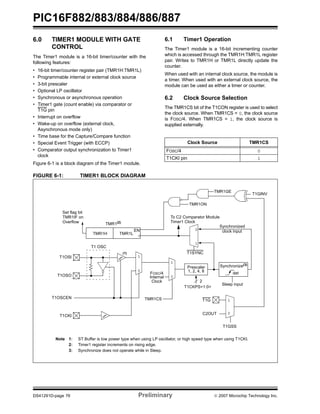


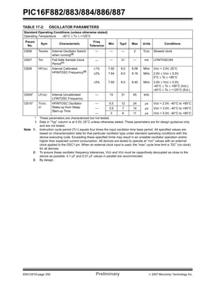
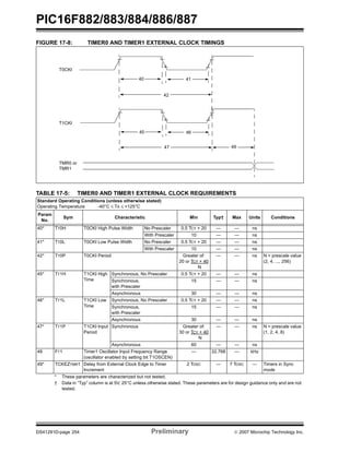
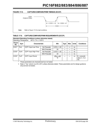
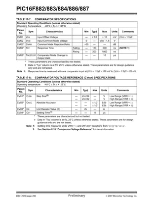
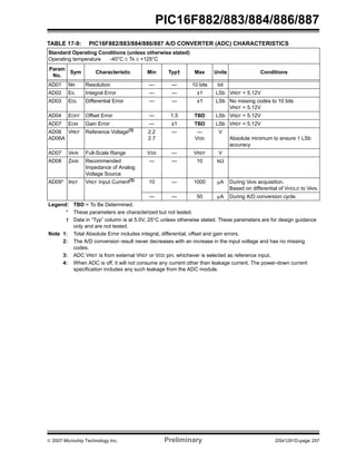
![PIC16F882/883/884/886/887
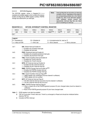
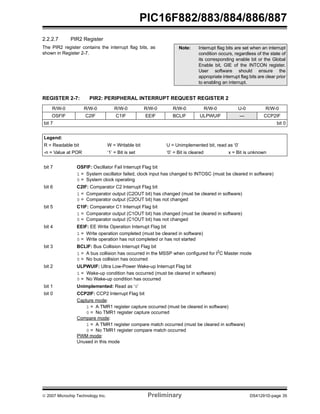
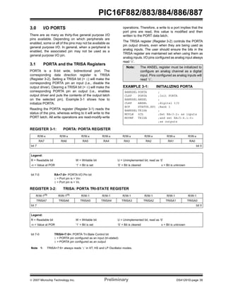
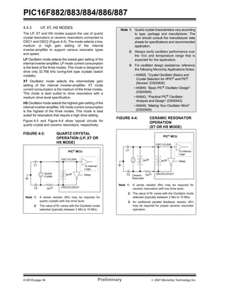
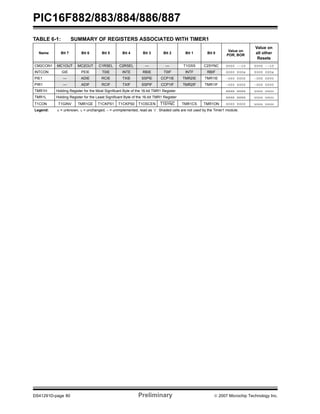
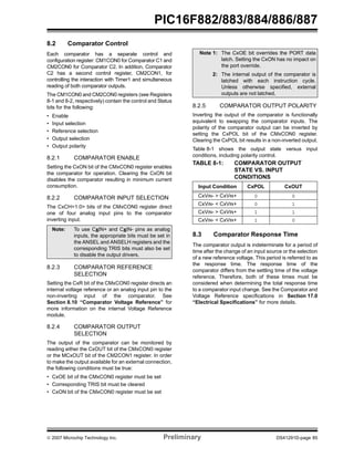
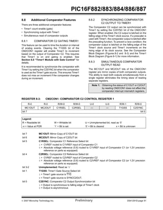
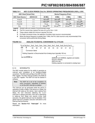
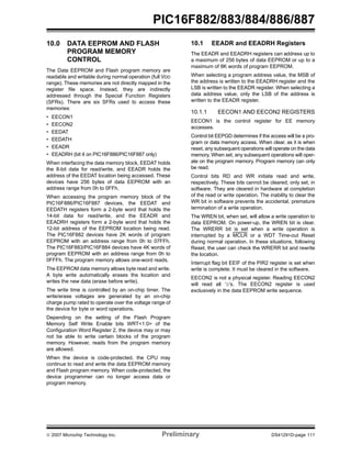
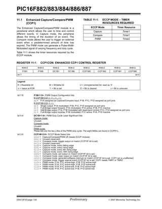
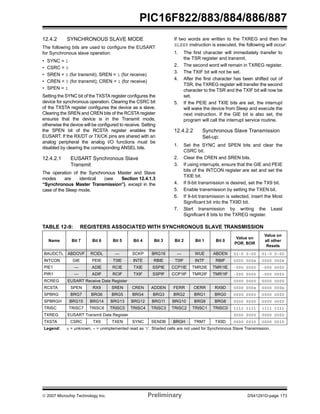
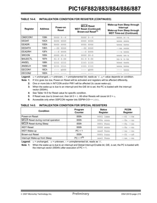
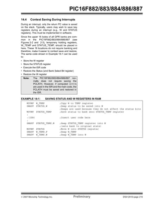
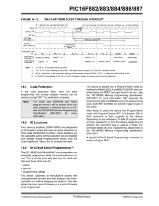
8.10 Comparator Voltage Reference
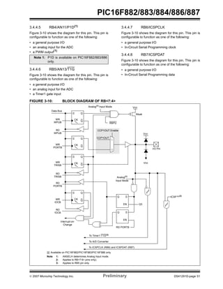
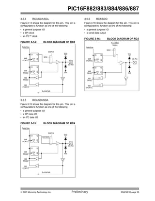
The Comparator Voltage Reference module provides
an internally generated voltage reference for the com-parators.
The following features are available:
• Independent from Comparator operation
• Two 16-level voltage ranges
• Output clamped to VSS
• Ratiometric with VDD
• Fixed Reference (0.6V)
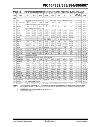
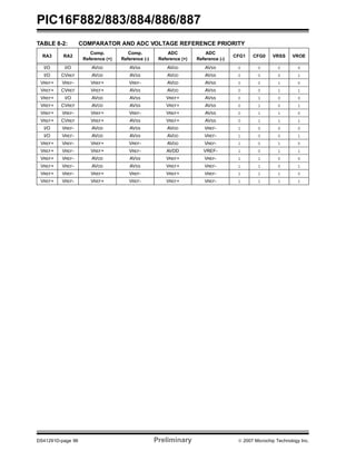
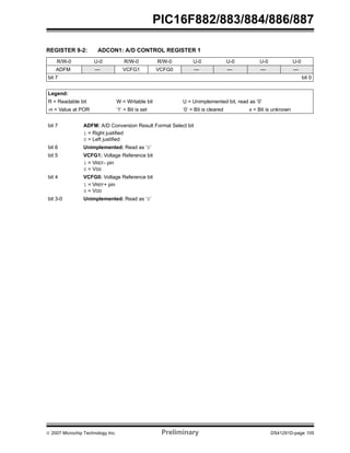
The VRCON register (Register 8-5) controls the
Voltage Reference module shown in Figure 8-8.
The voltage source is selectable through both ends of
the 16 connection resistor ladder network. Bit VRSS of
the VRCON register selects either the internal or
external voltage source.
The PIC16F883/884/886/887 allows the CVREF signal
to be output to the RA2 pin of PORTA under certain
configurations only. For more details, see Figure 8-9.
8.10.1 INDEPENDENT OPERATION
The comparator voltage reference is independent of
the comparator configuration. Setting the VREN bit of
the VRCON register will enable the voltage reference.
8.10.2 OUTPUT VOLTAGE SELECTION
The CVREF voltage reference has 2 ranges with 16
voltage levels in each range. Range selection is
controlled by the VRR bit of the VRCON register. The
16 levels are set with the VR<3:0> bits of the VRCON
register.
The CVREF output voltage is determined by the following
equations:
EQUATION 8-1: CVREF OUTPUT VOLTAGE
VRR = 1 (low range):
CVREF = (VR<3:0>/24) × VLADDER
VRR = 0 (high range):
CVREF = (VLADDER/4) +
(VR<3:0> × VLADDER/32)
VLADDER = VDD or ([VREF+] - [VREF-]) or VREF+
The full range of VSS to VDD cannot be realized due to
the construction of the module. See Figure 8-8.
8.10.3 OUTPUT CLAMPED TO VSS
The CVREF output voltage can be set to Vss with no
power consumption by configuring VRCON as follows:
• VREN=0
• VRR=1
• VR<3:0>=0000
This allows the comparator to detect a zero-crossing
while not consuming additional CVREF module current.
8.10.4 OUTPUT RATIOMETRIC TO VDD
The comparator voltage reference is VDD derived and
therefore, the CVREF output changes with fluctuations in
VDD. The tested absolute accuracy of the Comparator
Voltage Reference can be found in Section 17.0
“Electrical Specifications”.
8.10.5 FIXED VOLTAGE REFERENCE
The fixed voltage reference is independent of VDD, with
a nominal output voltage of 0.6V. This reference can be
enabled by setting the FVREN bit of the SRCON
register to ‘1’. This reference is always enabled when
the HFINTOSC oscillator is active.
8.10.6 FIXED VOLTAGE REFERENCE
STABILIZATION PERIOD
When the fixed Voltage Reference module is enabled,
it will require some time for the reference and its
amplifier circuits to stabilize. The user program must
include a small delay routine to allow the module to
settle. See the electrical specifications section for the
minimum delay requirement.
8.10.7 VOLTAGE REFERENCE
SELECTION
Multiplexers on the output of the Voltage Reference
module enable selection of either the CVREF or fixed
voltage reference for use by the comparators.
Setting the C1VREN bit of the VRCON register enables
current to flow in the CVREF voltage divider and selects
the CVREF voltage for use by C1. Clearing the C1VREN
bit selects the fixed voltage for use by C1.
Setting the C2VREN bit of the VRCON register enables
current to flow in the CVREF voltage divider and selects
the CVREF voltage for use by C2. Clearing the C2VREN
bit selects the fixed voltage for use by C2.
When both the C1VREN and C2VREN bits are cleared,
current flow in the CVREF voltage divider is disabled
minimizing the power drain of the voltage reference
peripheral.
DS41291D-page 94 Preliminary © 2007 Microchip Technology Inc.](https://image.slidesharecdn.com/pic16f887-140825175900-phpapp01/85/Pic16F887-96-320.jpg)

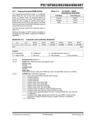
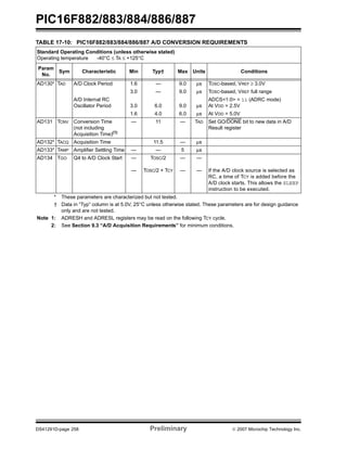
![PIC16F882/883/884/886/887
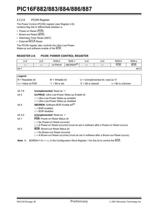
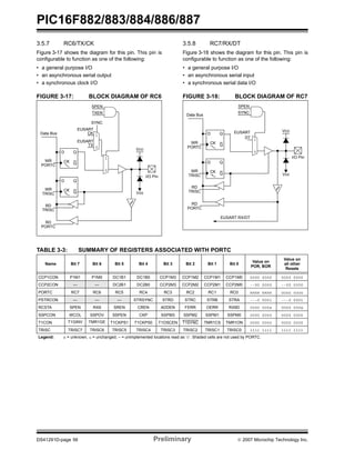
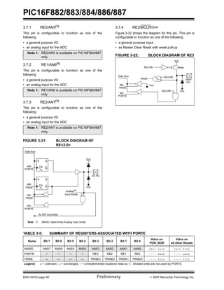
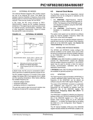
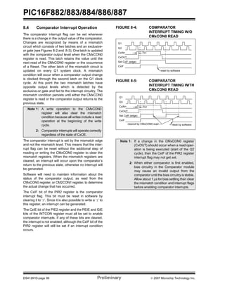
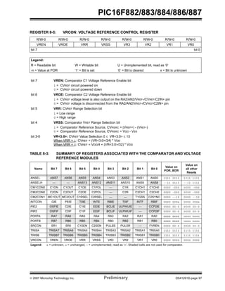
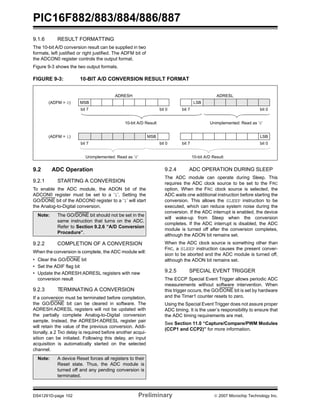
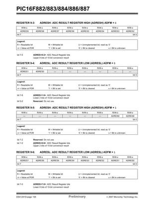
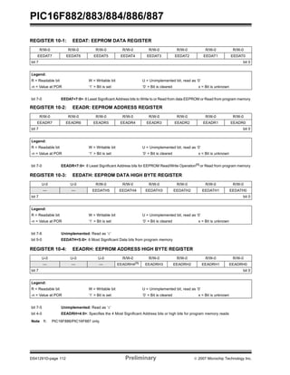
9.3 A/D Acquisition Requirements
For the ADC to meet its specified accuracy, the charge
holding capacitor (CHOLD) must be allowed to fully
charge to the input channel voltage level. The Analog
Input model is shown in Figure 9-4. The source
impedance (RS) and the internal sampling switch (RSS)
impedance directly affect the time required to charge the
capacitor CHOLD. The sampling switch (RSS) impedance
varies over the device voltage (VDD), see Figure 9-4.
The maximum recommended impedance for analog
sources is 10 kΩ. As the source impedance is
decreased, the acquisition time may be decreased.
After the analog input channel is selected (or changed),
an A/D acquisition must be done before the conversion
can be started. To calculate the minimum acquisition
time, Equation 9-1 may be used. This equation
assumes that 1/2 LSb error is used (1024 steps for the
ADC). The 1/2 LSb error is the maximum error allowed
for the ADC to meet its specified resolution.
EQUATION 9-1: ACQUISITION TIME EXAMPLE
Assumptions: Temperature = 50°C and external impedance of 10kΩ 5.0V VDD
TACQ Amplifier Settling Time Hold Capacitor Charging = + Time + Temperature Coefficient
= TAMP + TC + TCOFF
= 2μs + TC + [(Temperature - 25°C)(0.05μs/°C)]
The value for TC can be approximated with the following equations:
⎛ ⎞ = VCHOLD
⎝ – -----------⎠
VAPPLIED 1
1
2047
⎛ ⎞
⎜ ⎟
–
⎝ ⎠
VAPPLIED 1 e
–---------
TC
RC
⎛ ⎞
⎜ ⎟
–
⎝ ⎠
VAPPLIED 1 e
–Tc
RC
---------
= VCHOLD
= ⎛ ⎞
⎝ – -----------⎠
VAPPLIED 1
1
2047
Solving for TC:
TC = –CHOLD(RIC + RSS + RS) ln(1/2047)
= –10pF(1kΩ + 7kΩ + 10kΩ) ln(0.0004885)
= 1.37μs
Therefore:
TACQ = 2μS + 1.37μS + [(50°C- 25°C)(0.05μS/°C)]
= 4.67μS
;[1] VCHOLD charged to within 1/2 lsb
;[2] VCHOLD charge response to VAPPLIED
;combining [1] and [2]
Note 1: The reference voltage (VREF) has no effect on the equation, since it cancels itself out.
2: The charge holding capacitor (CHOLD) is not discharged after each conversion.
3: The maximum recommended impedance for analog sources is 10 kΩ. This is required to meet the pin
leakage specification.
© 2007 Microchip Technology Inc. Preliminary DS41291D-page 107](https://image.slidesharecdn.com/pic16f887-140825175900-phpapp01/85/Pic16F887-109-320.jpg)


![PIC16F882/883/884/886/887
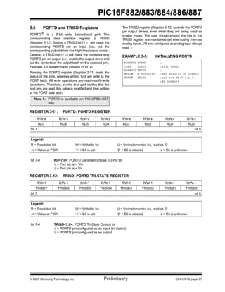
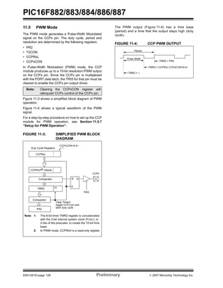
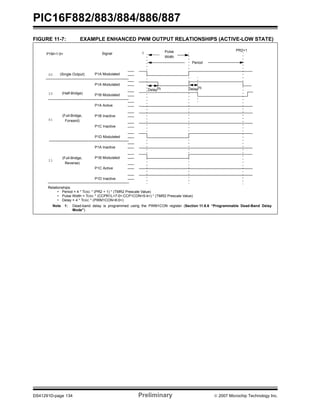
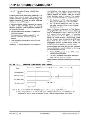
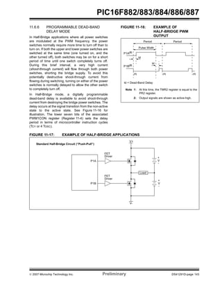
11.5.1 PWM PERIOD
The PWM period is specified by the PR2 register of
Timer2. The PWM period can be calculated using the
formula of Equation 11-1.
EQUATION 11-1: PWM PERIOD
PWM Period = [(PR2) + 1] • 4 • TOSC •
(TMR2 Prescale Value)
When TMR2 is equal to PR2, the following three events
occur on the next increment cycle:
• TMR2 is cleared
• The CCPx pin is set. (Exception: If the PWM duty
cycle = 0%, the pin will not be set.)
• The PWM duty cycle is latched from CCPRxL into
CCPRxH.
11.5.2 PWM DUTY CYCLE
The PWM duty cycle is specified by writing a 10-bit
value to multiple registers: CCPRxL register and
DCxB<1:0> bits of the CCPxCON register. The
CCPRxL contains the eight MSbs and the DCxB<1:0>
bits of the CCPxCON register contain the two LSbs.
CCPRxL and DCxB<1:0> bits of the CCPxCON
register can be written to at any time. The duty cycle
value is not latched into CCPRxH until after the period
completes (i.e., a match between PR2 and TMR2
registers occurs). While using the PWM, the CCPRxH
register is read-only.
Equation 11-2 is used to calculate the PWM pulse
width.
Equation 11-3 is used to calculate the PWM duty cycle
ratio.
EQUATION 11-2: PULSE WIDTH
Pulse Width = (CCPRxL:CCPxCON<5:4>) •
TOSC • (TMR2 Prescale Value)
EQUATION 11-3: DUTY CYCLE RATIO
Duty Cycle Ratio (CCPRxL:CCPxCON<5:4>)
= ----------------------------------------------------------------------
4(PR2 + 1)
The CCPRxH register and a 2-bit internal latch are
used to double buffer the PWM duty cycle. This double
buffering is essential for glitchless PWM operation.
The 8-bit timer TMR2 register is concatenated with
either the 2-bit internal system clock (FOSC), or 2 bits of
the prescaler, to create the 10-bit time base. The system
clock is used if the Timer2 prescaler is set to 1:1.
When the 10-bit time base matches the CCPRxH and
2-bit latch, then the CCPx pin is cleared (see
Figure 11-3).
Note: The Timer2 postscaler (see Section 7.1
“Timer2 Operation”) is not used in the
determination of the PWM frequency.
© 2007 Microchip Technology Inc. Preliminary DS41291D-page 129](https://image.slidesharecdn.com/pic16f887-140825175900-phpapp01/85/Pic16F887-131-320.jpg)
![PIC16F882/883/884/886/887
11.5.3 PWM RESOLUTION
The resolution determines the number of available duty
cycles for a given period. For example, a 10-bit resolution
will result in 1024 discrete duty cycles, whereas an 8-bit
resolution will result in 256 discrete duty cycles.
The maximum PWM resolution is 10 bits when PR2 is
255. The resolution is a function of the PR2 register
value as shown by Equation 11-4.
EQUATION 11-4: PWM RESOLUTION
Resolution log[4(PR2 + 1)]
= ------------------------------------------ bits
log(2)
Note: If the pulse width value is greater than the
period the assigned PWM pin(s) will
remain unchanged.
TABLE 11-3: EXAMPLE PWM FREQUENCIES AND RESOLUTIONS (FOSC = 20 MHz)
PWM Frequency 1.22 kHz 4.88 kHz 19.53 kHz 78.12 kHz 156.3 kHz 208.3 kHz
Timer Prescale (1, 4, 16) 16 4 1 1 1 1
PR2 Value 0xFF 0xFF 0xFF 0x3F 0x1F 0x17
Maximum Resolution (bits) 10 10 10 8 7 6.6
TABLE 11-4: EXAMPLE PWM FREQUENCIES AND RESOLUTIONS (FOSC = 8 MHz)
PWM Frequency 1.22 kHz 4.90 kHz 19.61 kHz 76.92 kHz 153.85 kHz 200.0 kHz
Timer Prescale (1, 4, 16) 16 4 1 1 1 1
PR2 Value 0x65 0x65 0x65 0x19 0x0C 0x09
Maximum Resolution (bits) 8 8 8 6 5 5
DS41291D-page 130 Preliminary © 2007 Microchip Technology Inc.](https://image.slidesharecdn.com/pic16f887-140825175900-phpapp01/85/Pic16F887-132-320.jpg)
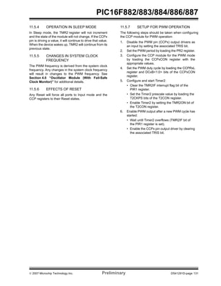
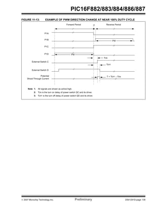
![PIC16F882/883/884/886/887
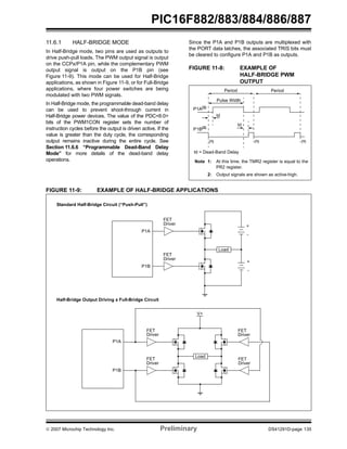
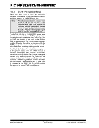
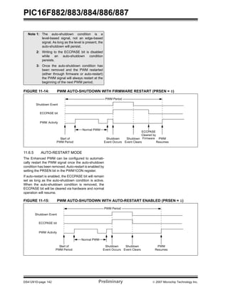
11.6.4 ENHANCED PWM
AUTO-SHUTDOWN MODE
The PWM mode supports an Auto-Shutdown mode that
will disable the PWM outputs when an external
shutdown event occurs. Auto-Shutdown mode places
the PWM output pins into a predetermined state. This
mode is used to help prevent the PWM from damaging
the application.
The auto-shutdown sources are selected using the
ECCPAS<2:0> bits of the ECCPAS register. A shutdown
event may be generated by:
• A logic ‘0’ on the INT pin
• Comparator C1
• Comparator C2
• Setting the ECCPASE bit in firmware
A shutdown condition is indicated by the ECCPASE
(Auto-Shutdown Event Status) bit of the ECCPAS
register. If the bit is a ‘0’, the PWM pins are operating
normally. If the bit is a ‘1’, the PWM outputs are in the
shutdown state.
When a shutdown event occurs, two things happen:
The ECCPASE bit is set to ‘1’. The ECCPASE will
remain set until cleared in firmware or an auto-restart
occurs (see Section 11.6.5 “Auto-Restart Mode”).
The enabled PWM pins are asynchronously placed in
their shutdown states. The PWM output pins are
grouped into pairs [P1A/P1C] and [P1B/P1D]. The state
of each pin pair is determined by the PSSAC and
PSSBD bits of the ECCPAS register. Each pin pair may
be placed into one of three states:
• Drive logic ‘1’
• Drive logic ‘0’
• Tri-state (high-impedance)
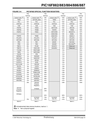
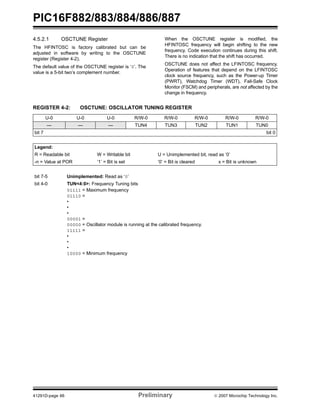
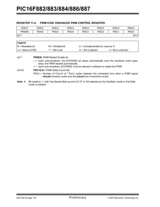
REGISTER 11-3: ECCPAS: ENHANCED CAPTURE/COMPARE/PWM AUTO-SHUTDOWN
CONTROL REGISTER
R/W-0 R/W-0 R/W-0 R/W-0 R/W-0 R/W-0 R/W-0 R/W-0
ECCPASE ECCPAS2 ECCPAS1 ECCPAS0 PSSAC1 PSSAC0 PSSBD1 PSSBD0
bit 7 bit 0
Legend:
R = Readable bit W = Writable bit U = Unimplemented bit, read as ‘0’
-n = Value at POR ‘1’ = Bit is set ‘0’ = Bit is cleared x = Bit is unknown
bit 7 ECCPASE: ECCP Auto-Shutdown Event Status bit
1 = A shutdown event has occurred; ECCP outputs are in shutdown state
0 = ECCP outputs are operating
bit 6-4 ECCPAS<2:0>: ECCP Auto-shutdown Source Select bits
000 = Auto-Shutdown is disabled
001 = Comparator C1 output change
010 = Comparator C2 output change(1)
011 = Either Comparator C1 or C2 change
100 = VIL on INT pin
101 = VIL on INT pin or Comparator C1 change
110 = VIL on INT pin or Comparator C2 change
111 = VIL on INT pin or Comparator C1 or Comparator C2 change
bit 3-2 PSSACn: Pins P1A and P1C Shutdown State Control bits
00 = Drive pins P1A and P1C to ‘0’
01 = Drive pins P1A and P1C to ‘1’
1x = Pins P1A and P1C tri-state
bit 1-0 PSSBDn: Pins P1B and P1D Shutdown State Control bits
00 = Drive pins P1B and P1D to ‘0’
01 = Drive pins P1B and P1D to ‘1’
1x = Pins P1B and P1D tri-state
Note 1: If C2SYNC is enabled, the shutdown will be delayed by Timer1.
© 2007 Microchip Technology Inc. Preliminary DS41291D-page 141](https://image.slidesharecdn.com/pic16f887-140825175900-phpapp01/85/Pic16F887-143-320.jpg)
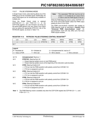
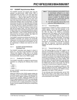
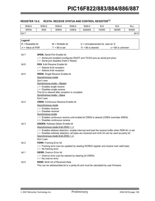
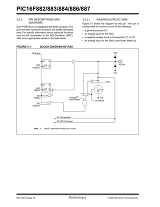
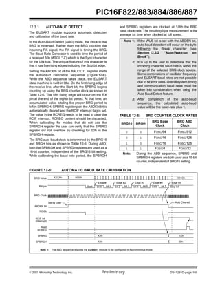
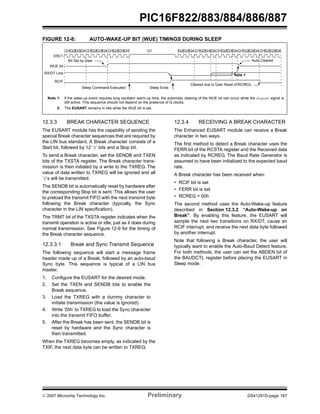
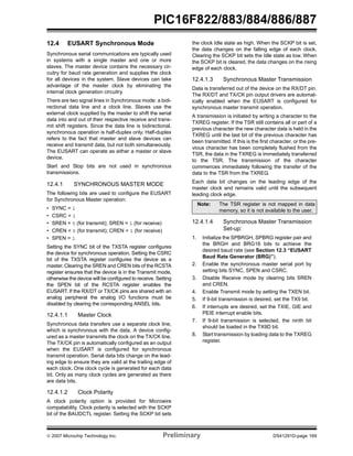
![PIC16F822/883/884/886/887
12.3 EUSART Baud Rate Generator
(BRG)
The Baud Rate Generator (BRG) is an 8-bit or 16-bit
timer that is dedicated to the support of both the
asynchronous and synchronous EUSART operation.
By default, the BRG operates in 8-bit mode. Setting the
BRG16 bit of the BAUDCTL register selects 16-bit
mode.
The SPBRGH, SPBRG register pair determines the
period of the free running baud rate timer. In
Asynchronous mode the multiplier of the baud rate
period is determined by both the BRGH bit of the TXSTA
register and the BRG16 bit of the BAUDCTL register. In
Synchronous mode, the BRGH bit is ignored.
Table 12-3 contains the formulas for determining the
baud rate. Example 12-1 provides a sample calculation
for determining the baud rate and baud rate error.
Typical baud rates and error values for various
asynchronous modes have been computed for your
convenience and are shown in Table 12-3. It may be
advantageous to use the high baud rate (BRGH = 1),
or the 16-bit BRG (BRG16 = 1) to reduce the baud rate
error. The 16-bit BRG mode is used to achieve slow
baud rates for fast oscillator frequencies.
Writing a new value to the SPBRGH, SPBRG register
pair causes the BRG timer to be reset (or cleared). This
ensures that the BRG does not wait for a timer overflow
before outputting the new baud rate.
If the system clock is changed during an active receive
operation, a receive error or data loss may result. To
avoid this problem, check the status of the RCIDL bit to
make sure that the receive operation is Idle before
changing the system clock.
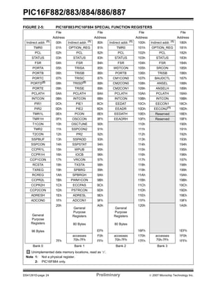
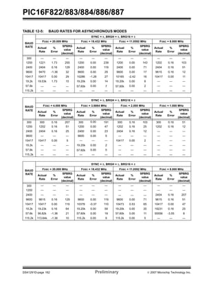
EXAMPLE 12-1: CALCULATING BAUD
RATE ERROR
TABLE 12-3: BAUD RATE FORMULAS
For a device with FOSC of 16 MHz, desired baud rate
of 9600, Asynchronous mode, 8-bit BRG:
Desired Baud Rate
= --------------------------------------------------------------------
64([SPBRGH:SPBRG] + 1)
Solving for SPBRGH:SPBRG:
X
FOSC
FOSC
---------------------------------------------
Desired Baud Rate
= --------------------------------------------- – 1
64
16000000
-----------------------
9600
= ----------------------- – 1
64
= [25.042] = 25
Calculated Baud Rate
16000000
64(25 + 1)
= ---------------------------
= 9615
Error
Calc. Baud Rate – Desired Baud Rate
= --------------------------------------------------------------------------------------------
Desired Baud Rate
(9615 – 9600)
= ---------------------------------- = 0.16%
9600
Configuration Bits
BRG/EUSART Mode Baud Rate Formula
SYNC BRG16 BRGH
0 0 0 8-bit/Asynchronous FOSC/[64 (n+1)]
0 0 1 8-bit/Asynchronous
FOSC/[16 (n+1)]
0 1 0 16-bit/Asynchronous
0 1 1 16-bit/Asynchronous
1 0 x 8-bit/Synchronous FOSC/[4 (n+1)]
1 1 x 16-bit/Synchronous
Legend: x = don’t care, n = value of SPBRGH, SPBRG register pair
TABLE 12-4: REGISTERS ASSOCIATED WITH THE BAUD RATE GENERATOR
Name Bit 7 Bit 6 Bit 5 Bit 4 Bit 3 Bit 2 Bit 1 Bit 0
Value on
POR, BOR
Value on
all other
Resets
BAUDCTL ABDOVF RCIDL — SCKP BRG16 — WUE ABDEN 01-0 0-00 01-0 0-00
RCSTA SPEN RX9 SREN CREN ADDEN FERR OERR RX9D 0000 000x 0000 000x
SPBRG BRG7 BRG6 BRG5 BRG4 BRG3 BRG2 BRG1 BRG0 0000 0000 0000 0000
SPBRGH BRG15 BRG14 BRG13 BRG12 BRG11 BRG10 BRG9 BRG8 0000 0000 0000 0000
TXSTA CSRC TX9 TXEN SYNC SENDB BRGH TRMT TX9D 0000 0010 0000 0010
Legend: x = unknown, – = unimplemented read as ‘0’. Shaded cells are not used for the Baud Rate Generator.
© 2007 Microchip Technology Inc. Preliminary DS41291D-page 161](https://image.slidesharecdn.com/pic16f887-140825175900-phpapp01/85/Pic16F887-163-320.jpg)


![PIC16F882/883/884/886/887
15.2 Instruction Descriptions
ADDLW Add literal and W
Syntax: [ label ] ADDLW k
Operands: 0 ≤ k ≤ 255
Operation: (W) + k → (W)
Status Affected: C, DC, Z
Description: The contents of the W register
are added to the eight-bit literal ‘k’
and the result is placed in the
W register.
ADDWF Add W and f
Syntax: [ label ] ADDWF f,d
Operands: 0 ≤ f ≤ 127
d ∈ [0,1]
Operation: (W) + (f) → (destination)
Status Affected: C, DC, Z
Description: Add the contents of the W register
with register ‘f’. If ‘d’ is ‘0’, the
result is stored in the W register. If
‘d’ is ‘1’, the result is stored back
in register ‘f’.
ANDLW AND literal with W
Syntax: [ label ] ANDLW k
Operands: 0 ≤ k ≤ 255
Operation: (W) .AND. (k) → (W)
Status Affected: Z
Description: The contents of W register are
AND’ed with the eight-bit literal
‘k’. The result is placed in the W
register.
ANDWF AND W with f
Syntax: [ label ] ANDWF f,d
Operands: 0 ≤ f ≤ 127
d ∈ [0,1]
Operation: (W) .AND. (f) → (destination)
Status Affected: Z
Description: AND the W register with register
‘f’. If ‘d’ is ‘0’, the result is stored in
the W register. If ‘d’ is ‘1’, the
result is stored back in register ‘f’.
BCF Bit Clear f
Syntax: [ label ] BCF f,b
Operands: 0 ≤ f ≤ 127
0 ≤ b ≤ 7
Operation: 0 → (f<b>)
Status Affected: None
Description: Bit ‘b’ in register ‘f’ is cleared.
BSF Bit Set f
Syntax: [ label ] BSF f,b
Operands: 0 ≤ f ≤ 127
0 ≤ b ≤ 7
Operation: 1 → (f<b>)
Status Affected: None
Description: Bit ‘b’ in register ‘f’ is set.
BTFSC Bit Test f, Skip if Clear
Syntax: [ label ] BTFSC f,b
Operands: 0 ≤ f ≤ 127
0 ≤ b ≤ 7
Operation: skip if (f<b>) = 0
Status Affected: None
Description: If bit ‘b’ in register ‘f’ is ‘1’, the next
instruction is executed.
If bit ‘b’ in register ‘f’ is ‘0’, the next
instruction is discarded, and a NOP
is executed instead, making this a
two-cycle instruction.
© 2007 Microchip Technology Inc. Preliminary DS41291D-page 227](https://image.slidesharecdn.com/pic16f887-140825175900-phpapp01/85/Pic16F887-229-320.jpg)
![PIC16F882/883/884/886/887
BTFSS Bit Test f, Skip if Set
Syntax: [ label ] BTFSS f,b
Operands: 0 ≤ f ≤ 127
0 ≤ b < 7
Operation: skip if (f<b>) = 1
Status Affected: None
Description: If bit ‘b’ in register ‘f’ is ‘0’, the next
instruction is executed.
If bit ‘b’ is ‘1’, then the next
instruction is discarded and a NOP
is executed instead, making this a
two-cycle instruction.
CALL Call Subroutine
Syntax: [ label ] CALL k
Operands: 0 ≤ k ≤ 2047
Operation: (PC)+ 1→ TOS,
k → PC<10:0>,
(PCLATH<4:3>) → PC<12:11>
Status Affected: None
Description: Call Subroutine. First, return
address (PC + 1) is pushed onto
the stack. The eleven-bit
immediate address is loaded into
PC bits <10:0>. The upper bits of
the PC are loaded from PCLATH.
CALL is a two-cycle instruction.
CLRF Clear f
Syntax: [ label ] CLRF f
Operands: 0 ≤ f ≤ 127
Operation: 00h → (f)
1 → Z
Status Affected: Z
Description: The contents of register ‘f’ are
cleared and the Z bit is set.
CLRW Clear W
Syntax: [ label ] CLRW
Operands: None
Operation: 00h → (W)
1 → Z
Status Affected: Z
Description: W register is cleared. Zero bit (Z)
is set.
CLRWDT Clear Watchdog Timer
Syntax: [ label ] CLRWDT
Operands: None
Operation: 00h → WDT
0 → WDT prescaler,
1 → TO
1 → PD
Status Affected: TO, PD
Description: CLRWDT instruction resets the
Watchdog Timer. It also resets the
prescaler of the WDT.
Status bits TO and PD are set.
COMF Complement f
Syntax: [ label ] COMF f,d
Operands: 0 ≤ f ≤ 127
d ∈ [0,1]
Operation: (f) → (destination)
Status Affected: Z
Description: The contents of register ‘f’ are
complemented. If ‘d’ is ‘0’, the
result is stored in W. If ‘d’ is ‘1’,
the result is stored back in
register ‘f’.
DECF Decrement f
Syntax: [ label ] DECF f,d
Operands: 0 ≤ f ≤ 127
d ∈ [0,1]
Operation: (f) - 1 → (destination)
Status Affected: Z
Description: Decrement register ‘f’. If ‘d’ is ‘0’,
the result is stored in the W
register. If ‘d’ is ‘1’, the result is
stored back in register ‘f’.
DS41291D-page 228 Preliminary © 2007 Microchip Technology Inc.](https://image.slidesharecdn.com/pic16f887-140825175900-phpapp01/85/Pic16F887-230-320.jpg)
![PIC16F882/883/884/886/887
DECFSZ Decrement f, Skip if 0
Syntax: [ label ] DECFSZ f,d
Operands: 0 ≤ f ≤ 127
d ∈ [0,1]
Operation: (f) - 1 → (destination);
skip if result = 0
Status Affected: None
Description: The contents of register ‘f’ are
decremented. If ‘d’ is ‘0’, the result
is placed in the W register. If ‘d’ is
‘1’, the result is placed back in
register ‘f’.
If the result is ‘1’, the next
instruction is executed. If the
result is ‘0’, then a NOP is
executed instead, making it a
two-cycle instruction.
GOTO Unconditional Branch
Syntax: [ label ] GOTO k
Operands: 0 ≤ k ≤ 2047
Operation: k → PC<10:0>
PCLATH<4:3> → PC<12:11>
Status Affected: None
Description: GOTO is an unconditional branch.
The eleven-bit immediate value is
loaded into PC bits <10:0>. The
upper bits of PC are loaded from
PCLATH<4:3>. GOTO is a
two-cycle instruction.
INCF Increment f
Syntax: [ label ] INCF f,d
Operands: 0 ≤ f ≤ 127
d ∈ [0,1]
Operation: (f) + 1 → (destination)
Status Affected: Z
Description: The contents of register ‘f’ are
incremented. If ‘d’ is ‘0’, the result
is placed in the W register. If ‘d’ is
‘1’, the result is placed back in
register ‘f’.
INCFSZ Increment f, Skip if 0
Syntax: [ label ] INCFSZ f,d
Operands: 0 ≤ f ≤ 127
d ∈ [0,1]
Operation: (f) + 1 → (destination),
skip if result = 0
Status Affected: None
Description: The contents of register ‘f’ are
incremented. If ‘d’ is ‘0’, the result
is placed in the W register. If ‘d’ is
‘1’, the result is placed back in
register ‘f’.
If the result is ‘1’, the next
instruction is executed. If the
result is ‘0’, a NOP is executed
instead, making it a two-cycle
instruction.
IORLW Inclusive OR literal with W
Syntax: [ label ] IORLW k
Operands: 0 ≤ k ≤ 255
Operation: (W) .OR. k → (W)
Status Affected: Z
Description: The contents of the W register are
OR’ed with the eight-bit literal ‘k’.
The result is placed in the
W register.
IORWF Inclusive OR W with f
Syntax: [ label ] IORWF f,d
Operands: 0 ≤ f ≤ 127
d ∈ [0,1]
Operation: (W) .OR. (f) → (destination)
Status Affected: Z
Description: Inclusive OR the W register with
register ‘f’. If ‘d’ is ‘0’, the result is
placed in the W register. If ‘d’ is
‘1’, the result is placed back in
register ‘f’.
© 2007 Microchip Technology Inc. Preliminary DS41291D-page 229](https://image.slidesharecdn.com/pic16f887-140825175900-phpapp01/85/Pic16F887-231-320.jpg)
![PIC16F882/883/884/886/887
MOVF Move f
Syntax: [ label ] MOVF f,d
Operands: 0 ≤ f ≤ 127
d ∈ [0,1]
Operation: (f) → (dest)
Status Affected: Z
Description: The contents of register ‘f’ is
moved to a destination dependent
upon the status of ‘d’. If d = 0,
destination is W register. If d = 1,
the destination is file register ‘f’
itself. d = 1 is useful to test a file
register since status flag Z is
affected.
Words: 1
Cycles: 1
Example: MOVF FSR, 0
After Instruction
W = value in FSR
register
Z = 1
MOVLW Move literal to W
Syntax: [ label ] MOVLW k
Operands: 0 ≤ k ≤ 255
Operation: k → (W)
Status Affected: None
Description: The eight-bit literal ‘k’ is loaded into
W register. The “don’t cares” will
assemble as ‘0’s.
Words: 1
Cycles: 1
Example: MOVLW 0x5A
After Instruction
W = 0x5A
MOVWF Move W to f
Syntax: [ label ] MOVWF f
Operands: 0 ≤ f ≤ 127
Operation: (W) → (f)
Status Affected: None
Description: Move data from W register to
register ‘f’.
Words: 1
Cycles: 1
Example: MOVW
F
OPTION
Before Instruction
OPTION = 0xFF
W = 0x4F
After Instruction
OPTION = 0x4F
W = 0x4F
NOP No Operation
Syntax: [ label ] NOP
Operands: None
Operation: No operation
Status Affected: None
Description: No operation.
Words: 1
Cycles: 1
Example: NOP
DS41291D-page 230 Preliminary © 2007 Microchip Technology Inc.](https://image.slidesharecdn.com/pic16f887-140825175900-phpapp01/85/Pic16F887-232-320.jpg)
![PIC16F882/883/884/886/887
RETFIE Return from Interrupt
Syntax: [ label ] RETFIE
Operands: None
Operation: TOS → PC,
1 → GIE
Status Affected: None
Description: Return from Interrupt. Stack is
POPed and Top-of-Stack (TOS) is
loaded in the PC. Interrupts are
enabled by setting Global
Interrupt Enable bit, GIE
(INTCON<7>). This is a two-cycle
instruction.
Words: 1
Cycles: 2
Example: RETFIE
After Interrupt
PC = TOS
GIE = 1
RETLW Return with literal in W
Syntax: [ label ] RETLW k
Operands: 0 ≤ k ≤ 255
Operation: k → (W);
TOS → PC
Status Affected: None
Description: The W register is loaded with the
eight-bit literal ‘k’. The program
counter is loaded from the top of
the stack (the return address).
This is a two-cycle instruction.
Words: 1
Cycles: 2
Example:
TABLE
CALL TABLE;W contains
table
;offset value
• ;W now has
• ;table value
•
•
ADDWF PC ;W = offset
RETLW k1 ;Begin table
RETLW k2 ;
•
•
•
RETLW kn ;End of table
Before Instruction
W = 0x07
After Instruction
W = value of k8
RETURN Return from Subroutine
Syntax: [ label ] RETURN
Operands: None
Operation: TOS → PC
Status Affected: None
Description: Return from subroutine. The stack
is POPed and the top of the stack
(TOS) is loaded into the program
counter. This is a two-cycle
instruction.
© 2007 Microchip Technology Inc. Preliminary DS41291D-page 231](https://image.slidesharecdn.com/pic16f887-140825175900-phpapp01/85/Pic16F887-233-320.jpg)
![PIC16F882/883/884/886/887
RLF Rotate Left f through Carry
Syntax: [ label ] RLF f,d
Operands: 0 ≤ f ≤ 127
d ∈ [0,1]
Operation: See description below
Status Affected: C
Description: The contents of register ‘f’ are
rotated one bit to the left through
the Carry flag. If ‘d’ is ‘0’, the
result is placed in the W register.
If ‘d’ is ‘1’, the result is stored
back in register ‘f’.
C Register f
Words: 1
Cycles: 1
Example: RLF REG1,0
Before Instruction
REG1 = 1110 0110
C = 0
After Instruction
REG1 = 1110 0110
W = 1100 1100
C = 1
RRF Rotate Right f through Carry
Syntax: [ label ] RRF f,d
Operands: 0 ≤ f ≤ 127
d ∈ [0,1]
Operation: See description below
Status Affected: C
Description: The contents of register ‘f’ are
rotated one bit to the right through
the Carry flag. If ‘d’ is ‘0’, the
result is placed in the W register.
If ‘d’ is ‘1’, the result is placed
back in register ‘f’.
C Register f
SLEEP Enter Sleep mode
Syntax: [ label ] SLEEP
Operands: None
Operation: 00h → WDT,
0 → WDT prescaler,
1 → TO,
0 → PD
Status Affected: TO, PD
Description: The power-down Status bit, PD is
cleared. Time-out Status bit, TO
is set. Watchdog Timer and its
prescaler are cleared.
The processor is put into Sleep
mode with the oscillator stopped.
SUBLW Subtract W from literal
Syntax: [ label ] SUBLW k
Operands: 0 ≤ k ≤ 255
Operation: k - (W) → (W)
Status Affected: C, DC, Z
Description: The W register is subtracted (2’s
complement method) from the
eight-bit literal ‘k’. The result is
placed in the W register.
C = 0 W > k
C = 1 W ≤ k
DC = 0 W<3:0> > k<3:0>
DC = 1 W<3:0> ≤ k<3:0>
DS41291D-page 232 Preliminary © 2007 Microchip Technology Inc.](https://image.slidesharecdn.com/pic16f887-140825175900-phpapp01/85/Pic16F887-234-320.jpg)
![PIC16F882/883/884/886/887
SUBWF Subtract W from f
Syntax: [ label ] SUBWF f,d
Operands: 0 ≤ f ≤ 127
d ∈ [0,1]
Operation: (f) - (W) → (destination)
Status Affected: C, DC, Z
Description: Subtract (2’s complement method)
W register from register ‘f’. If ‘d’ is
‘0’, the result is stored in the W
register. If ‘d’ is ‘1’, the result is
stored back in register ‘f’.
C = 0 W > f
C = 1 W ≤ f
DC = 0 W<3:0> > f<3:0>
DC = 1 W<3:0> ≤ f<3:0>
SWAPF Swap Nibbles in f
Syntax: [ label ] SWAPF f,d
Operands: 0 ≤ f ≤ 127
d ∈ [0,1]
Operation: (f<3:0>) → (destination<7:4>),
(f<7:4>) → (destination<3:0>)
Status Affected: None
Description: The upper and lower nibbles of
register ‘f’ are exchanged. If ‘d’ is
‘0’, the result is placed in the W
register. If ‘d’ is ‘1’, the result is
placed in register ‘f’.
XORLW Exclusive OR literal with W
Syntax: [ label ] XORLW k
Operands: 0 ≤ k ≤ 255
Operation: (W) .XOR. k → (W)
Status Affected: Z
Description: The contents of the W register
are XOR’ed with the eight-bit
literal ‘k’. The result is placed in
the W register.
XORWF Exclusive OR W with f
Syntax: [ label ] XORWF f,d
Operands: 0 ≤ f ≤ 127
d ∈ [0,1]
Operation: (W) .XOR. (f) → (destination)
Status Affected: Z
Description: Exclusive OR the contents of the
W register with register ‘f’. If ‘d’ is
‘0’, the result is stored in the W
register. If ‘d’ is ‘1’, the result is
stored back in register ‘f’.
© 2007 Microchip Technology Inc. Preliminary DS41291D-page 233](https://image.slidesharecdn.com/pic16f887-140825175900-phpapp01/85/Pic16F887-235-320.jpg)


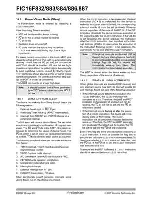
![PIC16F882/883/884/886/887
19.2 Package Details
The following sections give the technical details of the packages.
28-Lead Skinny Plastic Dual In-Line (SP or PJ) – 300 mil Body [SPDIP]
Note: For the most current package drawings, please see the Microchip Packaging Specification located at
http://www.microchip.com/packaging
E1
L
A2
A
3
A1 b1
b e
Units INCHES
E
eB
Dimension Limits MIN NOM MAX
D
Number of Pins N 28
Pitch e .100 BSC
Top to Seating Plane A – – .200
Molded Package Thickness A2 .120 .135 .150
Base to Seating Plane A1 .015 – –
Shoulder to Shoulder Width E .290 .310 .335
Molded Package Width E1 .240 .285 .295
Overall Length D 1.345 1.365 1.400
Tip to Seating Plane L .110 .130 .150
Lead Thickness c .008 .010 .015
Upper Lead Width b1 .040 .050 .070
Lower Lead Width b .014 .018 .022
Overall Row Spacing § eB – – .430
NOTE 1
N
1 2
c
Notes:
1. Pin 1 visual index feature may vary, but must be located within the hatched area.
2. § Significant Characteristic.
3. Dimensions D and E1 do not include mold flash or protrusions. Mold flash or protrusions shall not exceed .010" per side.
4. Dimensioning and tolerancing per ASME Y14.5M.
BSC: Basic Dimension. Theoretically exact value shown without tolerances.
Microchip Technology Drawing C04-070B
© 2007 Microchip Technology Inc. Preliminary DS41291D-page 265](https://image.slidesharecdn.com/pic16f887-140825175900-phpapp01/85/Pic16F887-267-320.jpg)
![PIC16F882/883/884/886/887
28-Lead Plastic Small Outline (SO or OI) – Wide, 7.50 mm Body [SOIC]
Note: For the most current package drawings, please see the Microchip Packaging Specification located at
http://www.microchip.com/packaging
h
h
L
L1
E1
A2
E
φ
α
Units MILLIMETERS
e
β
Dimension Limits MIN NOM MAX
NOTE 1
A
A1
N
1 2 3
b
D
Number of Pins N 28
Pitch e 1.27 BSC
Overall Height A – – 2.65
Molded Package Thickness A2 2.05 – –
Standoff § A1 0.10 – 0.30
Overall Width E 10.30 BSC
Molded Package Width E1 7.50 BSC
Overall Length D 17.90 BSC
Chamfer (optional) h 0.25 – 0.75
Foot Length L 0.40 – 1.27
Footprint L1 1.40 REF
Foot Angle Top φ 0° – 8°
Lead Thickness c 0.18 – 0.33
Lead Width b 0.31 – 0.51
Mold Draft Angle Top α 5° – 15°
Mold Draft Angle Bottom β 5° – 15°
c
Notes:
1. Pin 1 visual index feature may vary, but must be located within the hatched area.
2. § Significant Characteristic.
3. Dimensions D and E1 do not include mold flash or protrusions. Mold flash or protrusions shall not exceed 0.15 mm per side.
4. Dimensioning and tolerancing per ASME Y14.5M.
BSC: Basic Dimension. Theoretically exact value shown without tolerances.
REF: Reference Dimension, usually without tolerance, for information purposes only.
Microchip Technology Drawing C04-052B
DS41291D-page 266 Preliminary © 2007 Microchip Technology Inc.](https://image.slidesharecdn.com/pic16f887-140825175900-phpapp01/85/Pic16F887-268-320.jpg)
![PIC16F882/883/884/886/887
28-Lead Plastic Shrink Small Outline (SS) – 5.30 mm Body [SSOP]
Note: For the most current package drawings, please see the Microchip Packaging Specification located at
http://www.microchip.com/packaging
φ
L1 L
c
E
A2
E1
Units MILLIMETERS
e
Dimension Limits MIN NOM MAX
D
N
1 2
NOTE 1
b
Number of Pins N 28
Pitch e 0.65 BSC
Overall Height A – – 2.00
Molded Package Thickness A2 1.65 1.75 1.85
Standoff A1 0.05 – –
Overall Width E 7.40 7.80 8.20
Molded Package Width E1 5.00 5.30 5.60
Overall Length D 9.90 10.20 10.50
Foot Length L 0.55 0.75 0.95
Footprint L1 1.25 REF
Lead Thickness c 0.09 – 0.25
Foot Angle φ 0° 4° 8°
Lead Width b 0.22 – 0.38
A
A1
Notes:
1. Pin 1 visual index feature may vary, but must be located within the hatched area.
2. Dimensions D and E1 do not include mold flash or protrusions. Mold flash or protrusions shall not exceed 0.20 mm per side.
3. Dimensioning and tolerancing per ASME Y14.5M.
BSC: Basic Dimension. Theoretically exact value shown without tolerances.
REF: Reference Dimension, usually without tolerance, for information purposes only.
Microchip Technology Drawing C04-073B
© 2007 Microchip Technology Inc. Preliminary DS41291D-page 267](https://image.slidesharecdn.com/pic16f887-140825175900-phpapp01/85/Pic16F887-269-320.jpg)
![PIC16F882/883/884/886/887
28-Lead Plastic Quad Flat, No Lead Package (MM) – 6x6x0.9 mm Body [QFN-S]
with 0.40 mm Contact Length
Note: For the most current package drawings, please see the Microchip Packaging Specification located at
http://www.microchip.com/packaging
EXPOSED
PAD
E2
2
1
D2
N
NOTE 1
TOP VIEW BOTTOM VIEW
Units MILLIMETERS
E
2
1
L
A
A1
Dimension Limits MIN NOM MAX
D
N
Number of Pins N 28
Pitch e 0.65 BSC
Overall Height A 0.80 0.90 1.00
Standoff A1 0.00 0.02 0.05
Contact Thickness A3 0.20 REF
Overall Width E 6.00 BSC
Exposed Pad Width E2 3.65 3.70 4.70
Overall Length D 6.00 BSC
Exposed Pad Length D2 3.65 3.70 4.70
Contact Width b 0.23 0.38 0.43
Contact Length L 0.30 0.40 0.50
Contact-to-Exposed Pad K 0.20 – –
A3
Notes:
1. Pin 1 visual index feature may vary, but must be located within the hatched area.
2. Package is saw singulated.
3. Dimensioning and tolerancing per ASME Y14.5M.
BSC: Basic Dimension. Theoretically exact value shown without tolerances.
REF: Reference Dimension, usually without tolerance, for information purposes only.
e
b
K
Microchip Technology Drawing C04-124B
DS41291D-page 268 Preliminary © 2007 Microchip Technology Inc.](https://image.slidesharecdn.com/pic16f887-140825175900-phpapp01/85/Pic16F887-270-320.jpg)
![PIC16F882/883/884/886/887
40-Lead Plastic Dual In-Line (P or PL) – 600 mil Body [PDIP]
Note: For the most current package drawings, please see the Microchip Packaging Specification located at
http://www.microchip.com/packaging
E1
b e
L
A2
Units INCHES
E
eB
Dimension Limits MIN NOM MAX
D
1 2 3
b1
Number of Pins N 40
Pitch e .100 BSC
Top to Seating Plane A – – .250
Molded Package Thickness A2 .125 – .195
Base to Seating Plane A1 .015 – –
Shoulder to Shoulder Width E .590 – .625
Molded Package Width E1 .485 – .580
Overall Length D 1.980 – 2.095
Tip to Seating Plane L .115 – .200
Lead Thickness c .008 – .015
Upper Lead Width b1 .030 – .070
Lower Lead Width b .014 – .023
Overall Row Spacing § eB – – .700
N
NOTE 1
A
A1
c
Notes:
1. Pin 1 visual index feature may vary, but must be located within the hatched area.
2. § Significant Characteristic.
3. Dimensions D and E1 do not include mold flash or protrusions. Mold flash or protrusions shall not exceed .010" per side.
4. Dimensioning and tolerancing per ASME Y14.5M.
BSC: Basic Dimension. Theoretically exact value shown without tolerances.
Microchip Technology Drawing C04-016B
© 2007 Microchip Technology Inc. Preliminary DS41291D-page 269](https://image.slidesharecdn.com/pic16f887-140825175900-phpapp01/85/Pic16F887-271-320.jpg)
![PIC16F882/883/884/886/887
44-Lead Plastic Quad Flat, No Lead Package (ML) – 8x8 mm Body [QFN]
Note: For the most current package drawings, please see the Microchip Packaging Specification located at
http://www.microchip.com/packaging
EXPOSED
PAD
D2
E2
2
1
N
NOTE 1
TOP VIEW BOTTOM VIEW
Units MILLIMETERS
L
2
1
E
A3 A1
A
Dimension Limits MIN NOM MAX
D
N
Number of Pins N 44
Pitch e 0.65 BSC
Overall Height A 0.80 0.90 1.00
Standoff A1 0.00 0.02 0.05
Contact Thickness A3 0.20 REF
Overall Width E 8.00 BSC
Exposed Pad Width E2 6.30 6.45 6.80
Overall Length D 8.00 BSC
Exposed Pad Length D2 6.30 6.45 6.80
Contact Width b 0.25 0.30 0.38
Contact Length L 0.30 0.40 0.50
Contact-to-Exposed Pad K 0.20 – –
Notes:
1. Pin 1 visual index feature may vary, but must be located within the hatched area.
2. Package is saw singulated.
3. Dimensioning and tolerancing per ASME Y14.5M.
BSC: Basic Dimension. Theoretically exact value shown without tolerances.
REF: Reference Dimension, usually without tolerance, for information purposes only.
e
b
K
Microchip Technology Drawing C04-103B
DS41291D-page 270 Preliminary © 2007 Microchip Technology Inc.](https://image.slidesharecdn.com/pic16f887-140825175900-phpapp01/85/Pic16F887-272-320.jpg)
![PIC16F882/883/884/886/887
44-Lead Plastic Thin Quad Flatpack (PT) – 10x10x1 mm Body, 2.00 mm Footprint [TQFP]
Note: For the most current package drawings, please see the Microchip Packaging Specification located at
http://www.microchip.com/packaging
A
E
E1
NOTE 2
A1
L
L1
φ
Units MILLIMETERS
α
Dimension Limits MIN NOM MAX
D
D1
e
b
N
NOTE 1
1 2 3
β
Number of Leads N 44
Lead Pitch e 0.80 BSC
Overall Height A – – 1.20
Molded Package Thickness A2 0.95 1.00 1.05
Standoff A1 0.05 – 0.15
Foot Length L 0.45 0.60 0.75
Footprint L1 1.00 REF
Foot Angle φ 0° 3.5° 7°
Overall Width E 12.00 BSC
Overall Length D 12.00 BSC
Molded Package Width E1 10.00 BSC
Molded Package Length D1 10.00 BSC
Lead Thickness c 0.09 – 0.20
Lead Width b 0.30 0.37 0.45
Mold Draft Angle Top α 11° 12° 13°
Mold Draft Angle Bottom β 11° 12° 13°
c
A2
Notes:
1. Pin 1 visual index feature may vary, but must be located within the hatched area.
2. Chamfers at corners are optional; size may vary.
3. Dimensions D1 and E1 do not include mold flash or protrusions. Mold flash or protrusions shall not exceed 0.25 mm per side.
4. Dimensioning and tolerancing per ASME Y14.5M.
BSC: Basic Dimension. Theoretically exact value shown without tolerances.
REF: Reference Dimension, usually without tolerance, for information purposes only.
Microchip Technology Drawing C04-076B
© 2007 Microchip Technology Inc. Preliminary DS41291D-page 271](https://image.slidesharecdn.com/pic16f887-140825175900-phpapp01/85/Pic16F887-273-320.jpg)