Download to read offline
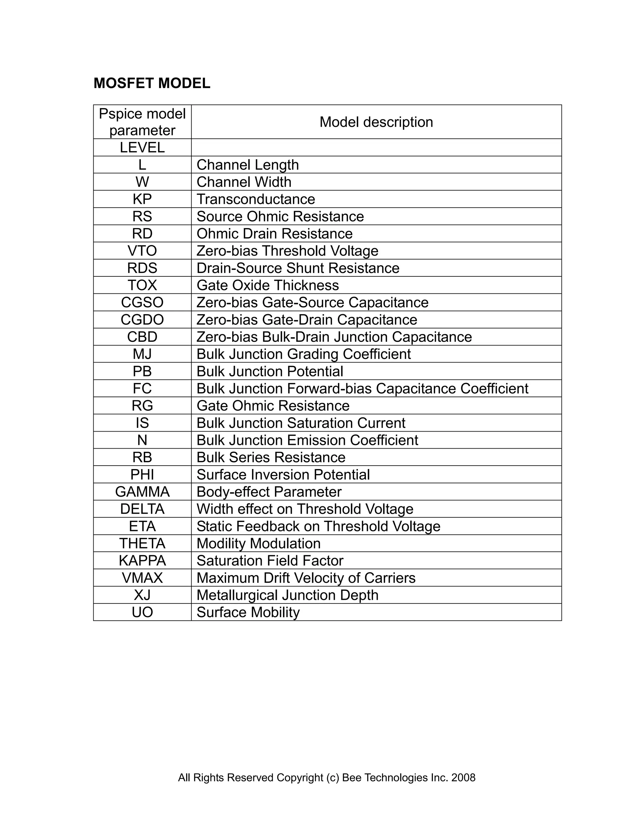
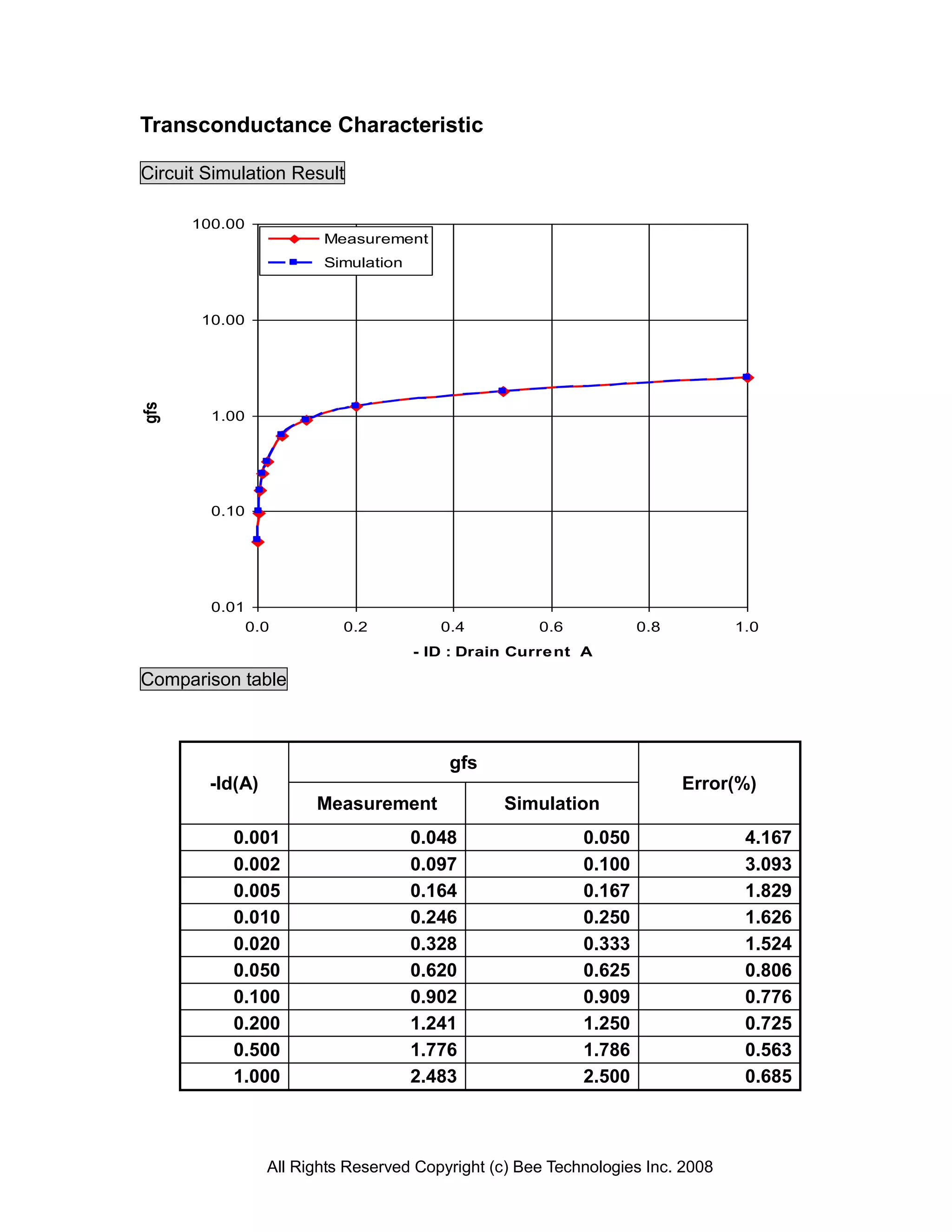
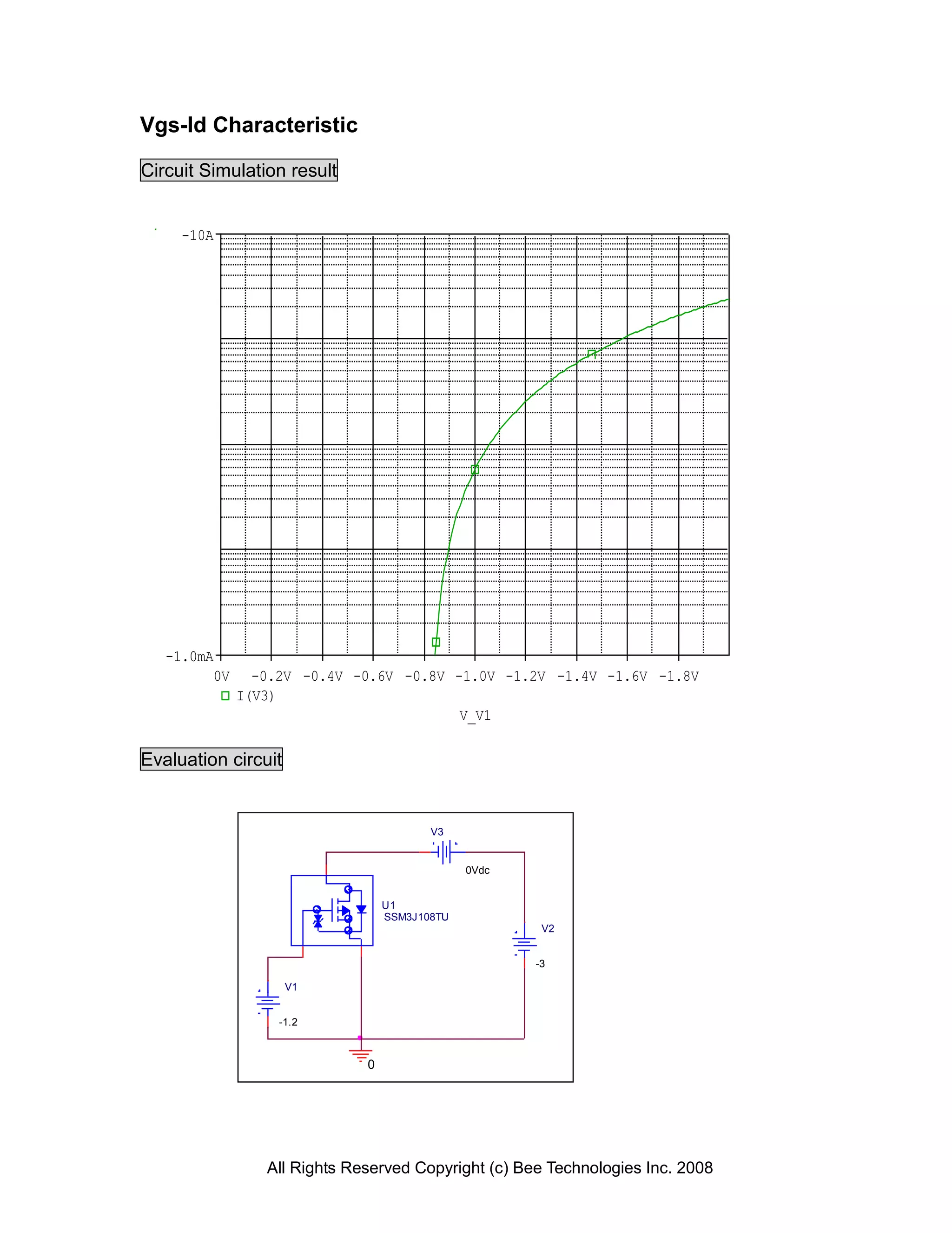
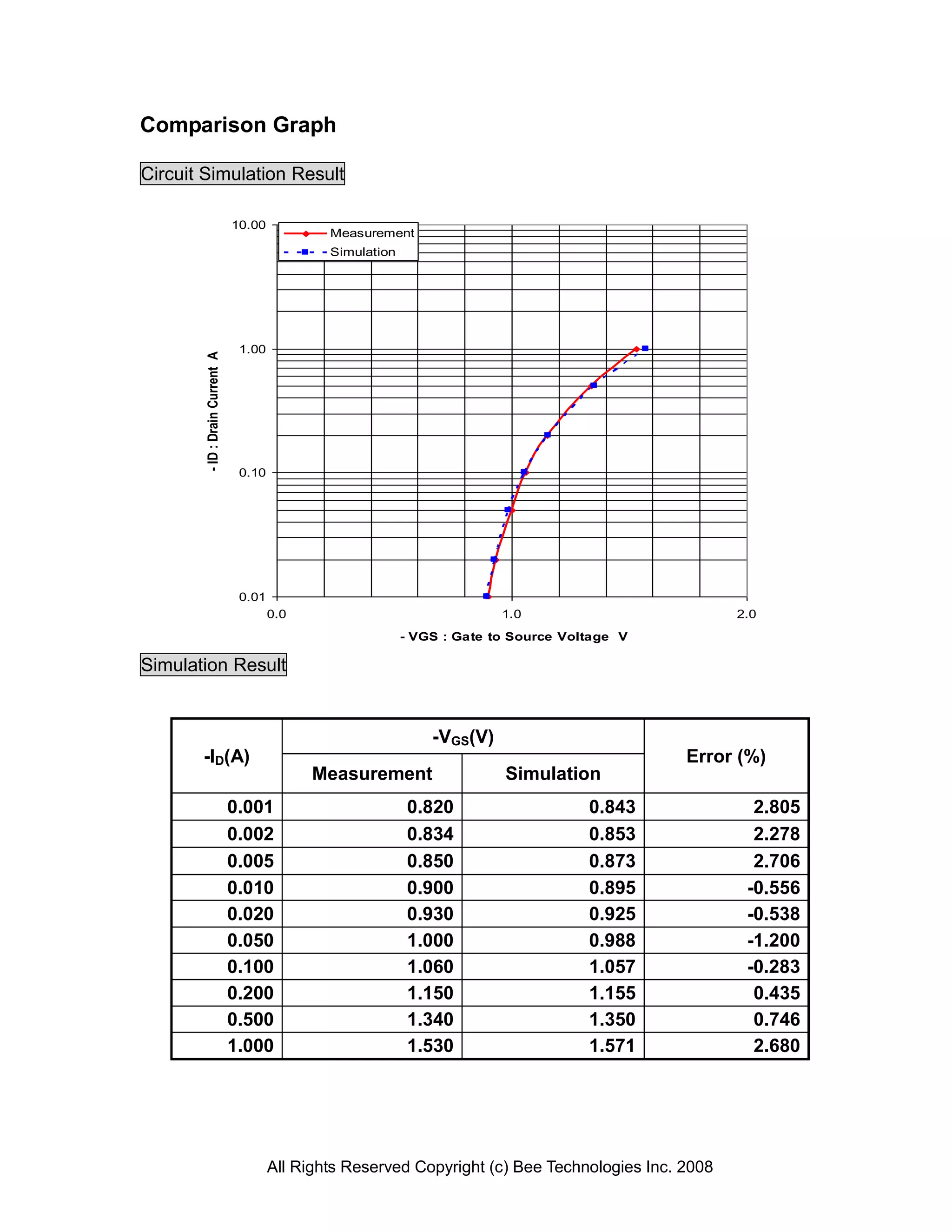
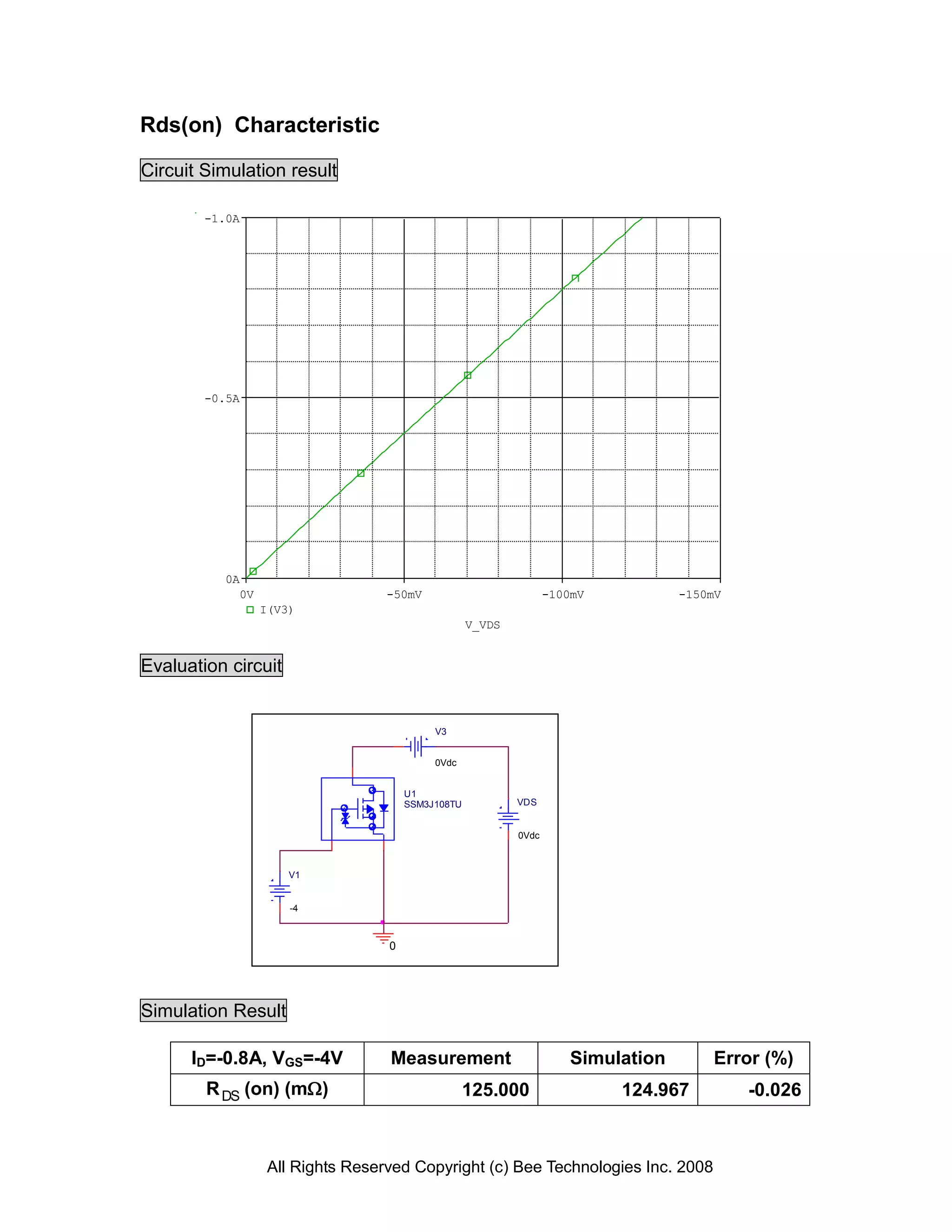
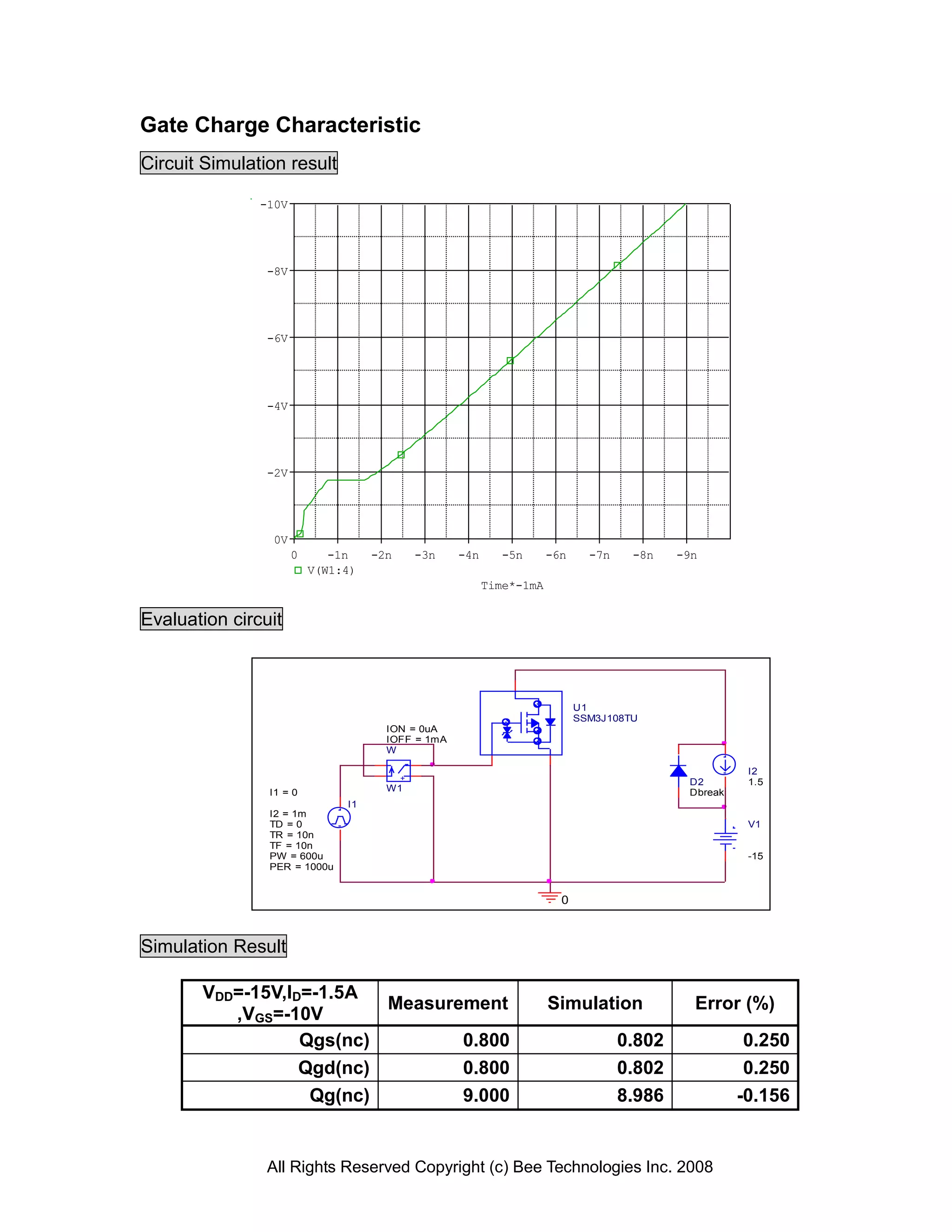
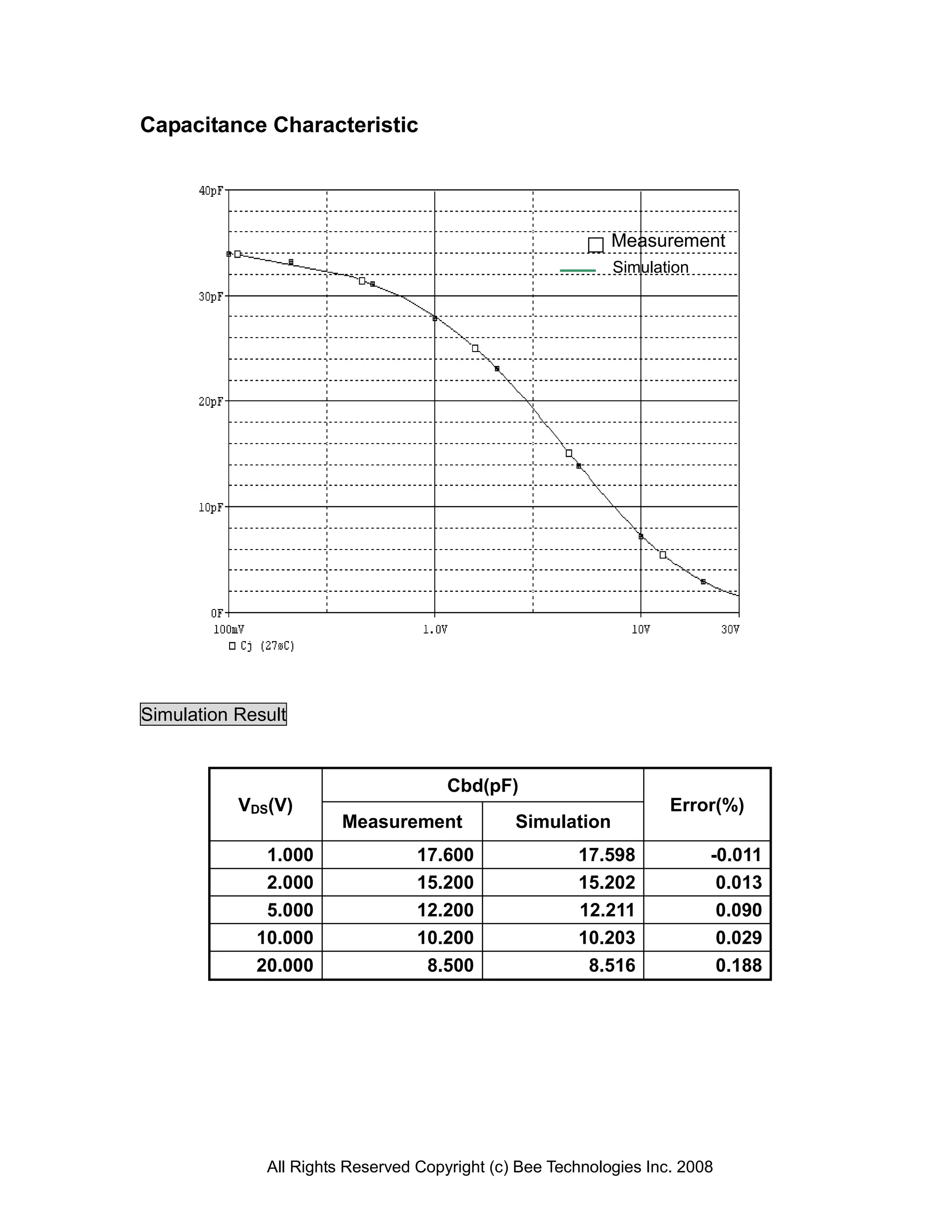
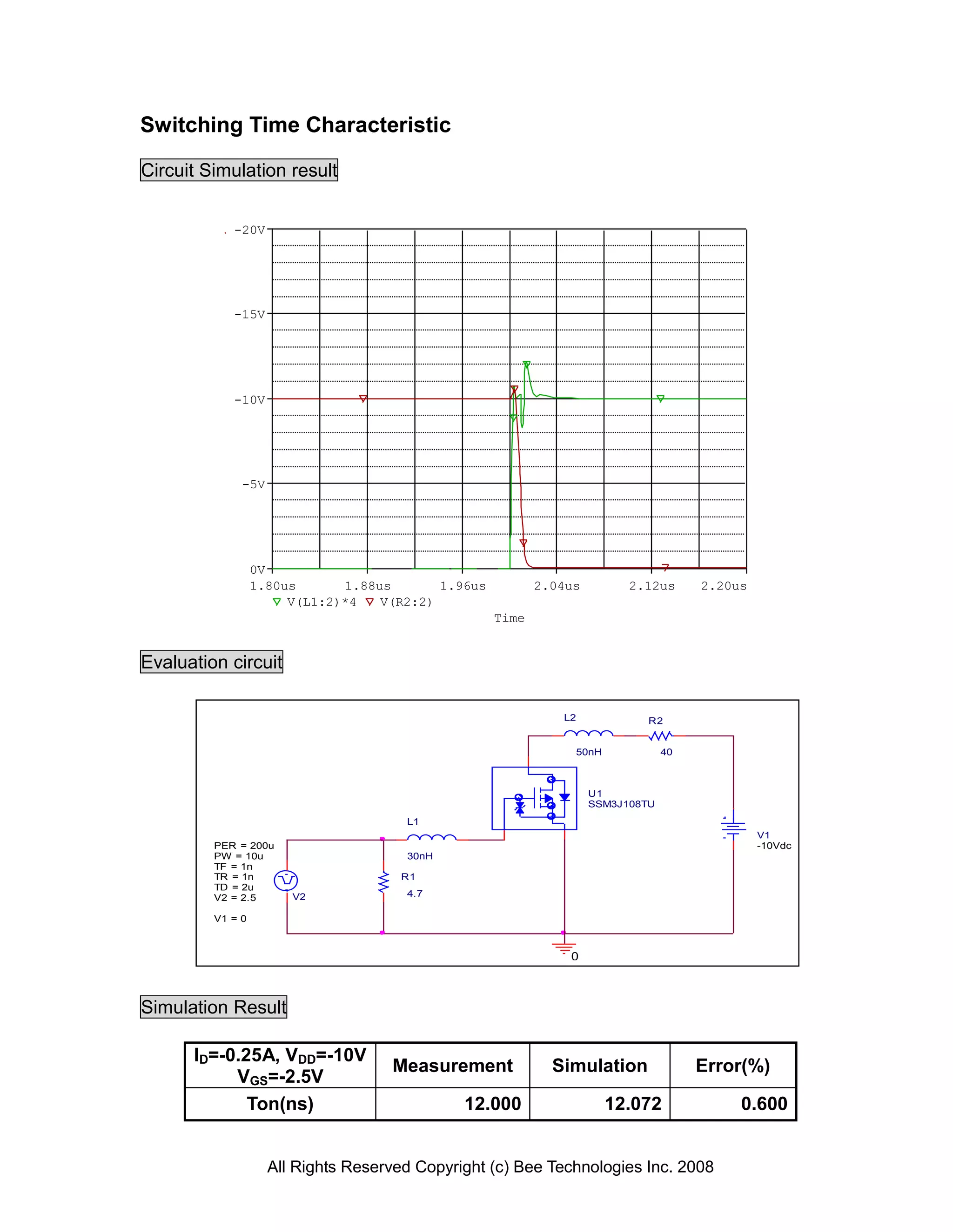
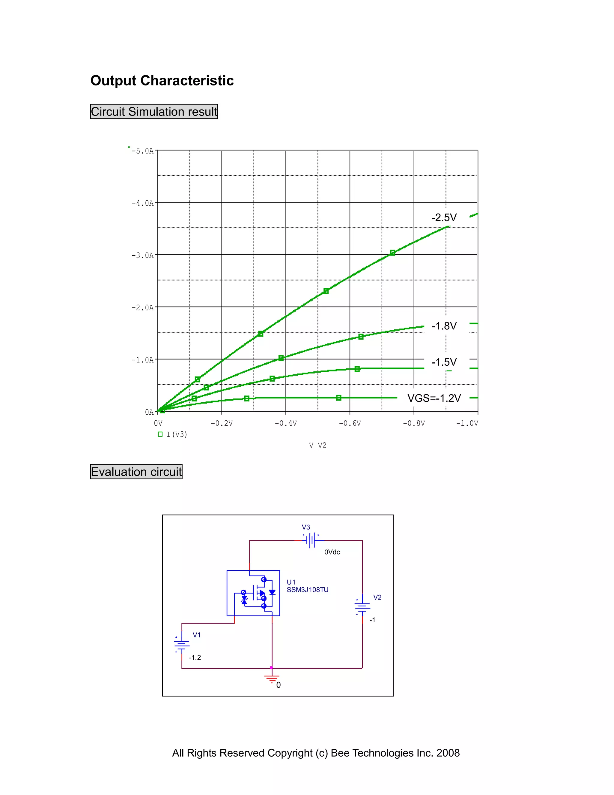
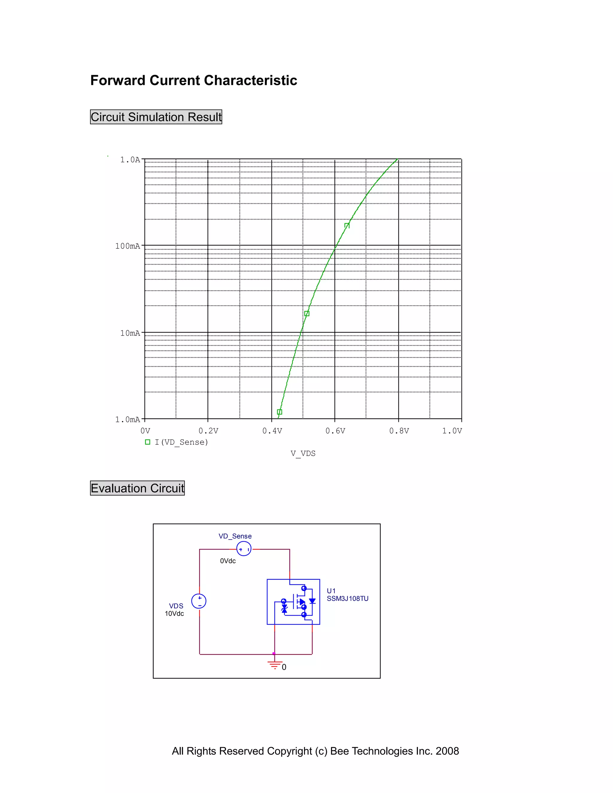
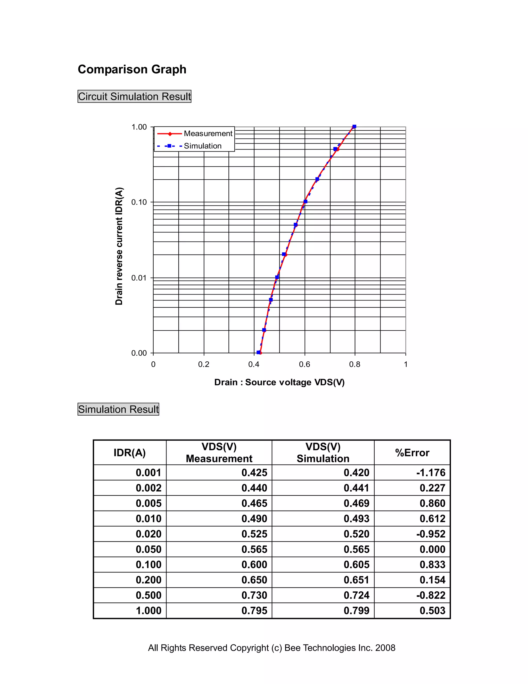
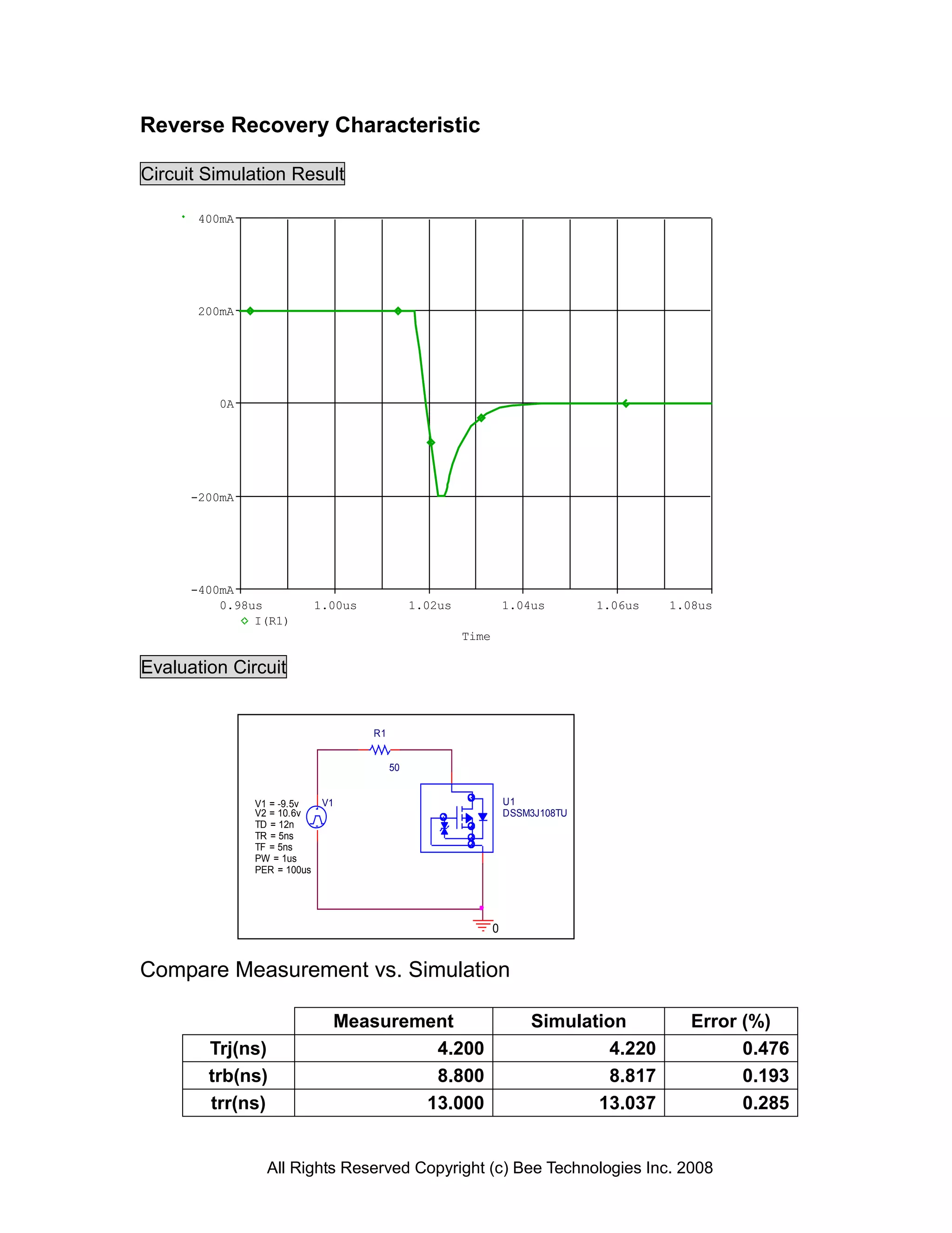
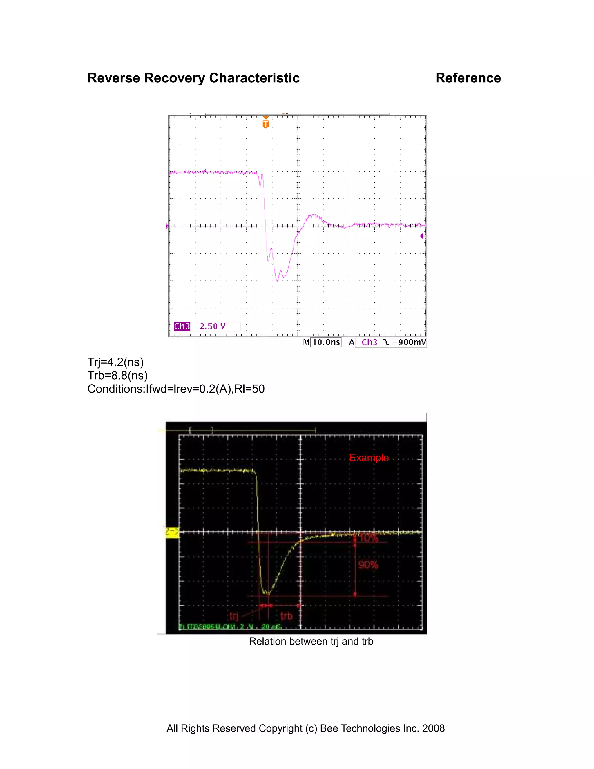
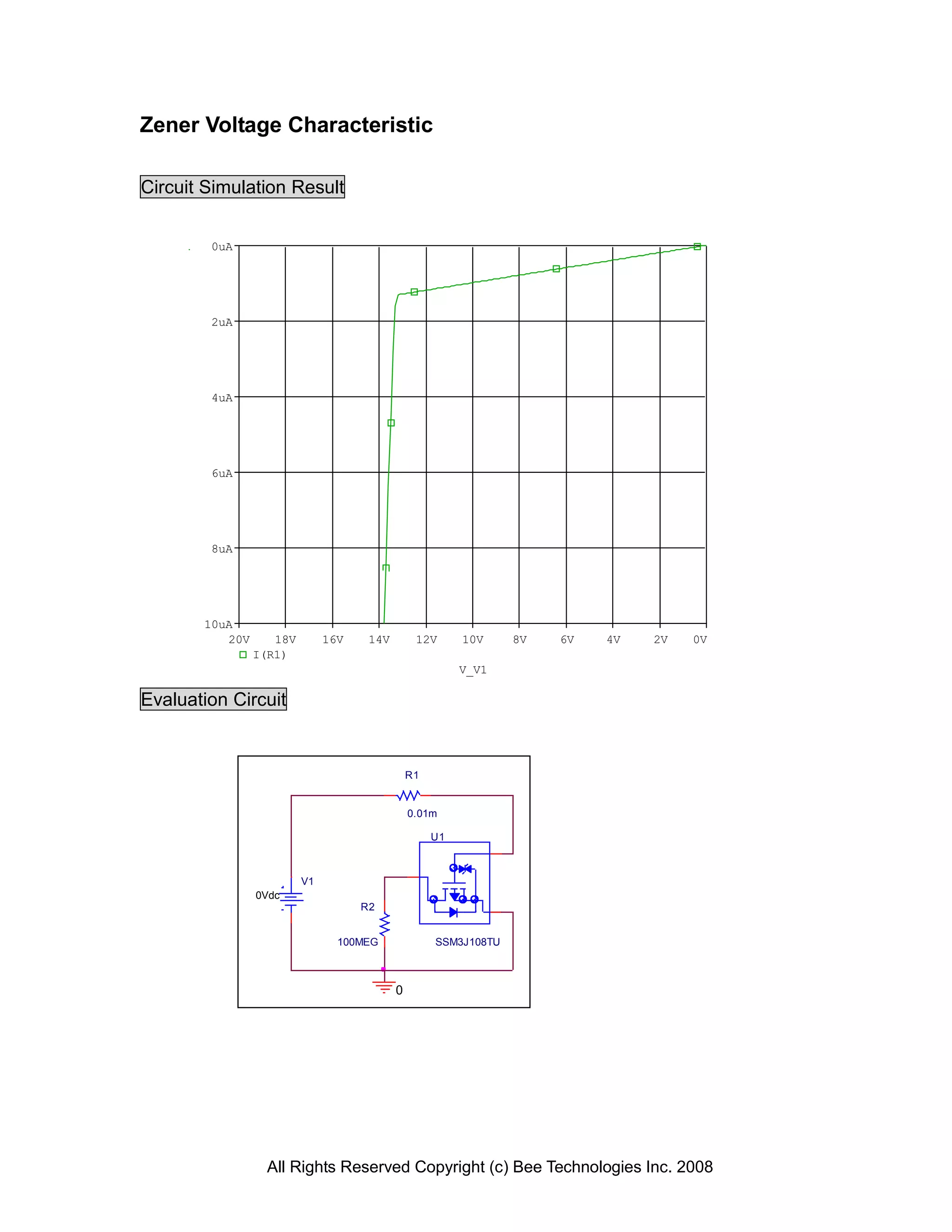
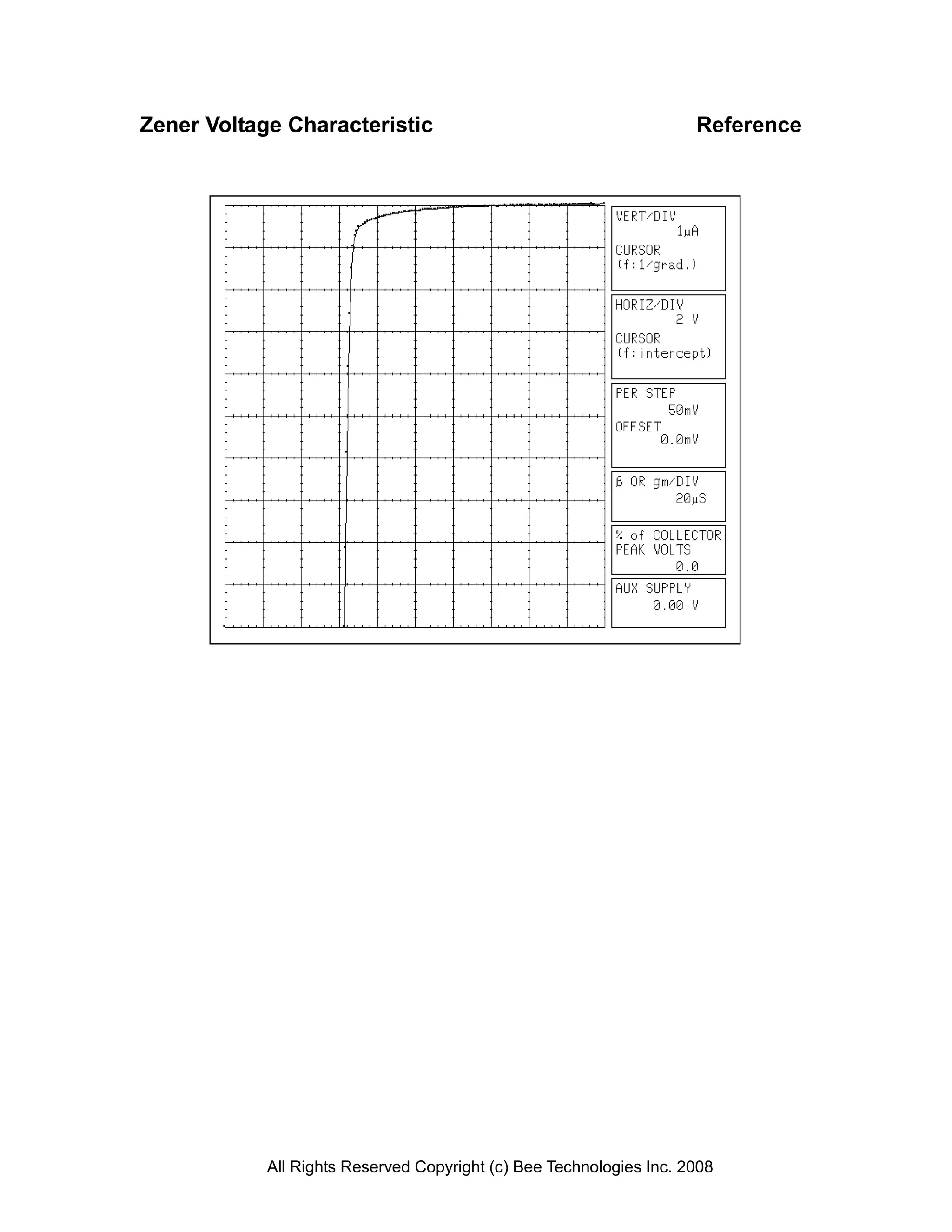

The document is a comprehensive device modeling report for the SSM3J108TU power MOSFET by Toshiba, detailing key parameters such as channel dimensions, transconductance, and various resistances. It includes simulation results comparing measurements of drain current, gate charge characteristics, and switching times against theoretical predictions, showcasing the accuracy of the models used. Additionally, the report covers forward and reverse recovery characteristics along with zener voltage characteristics, offering a thorough analysis of the device's performance.


