Download to read offline
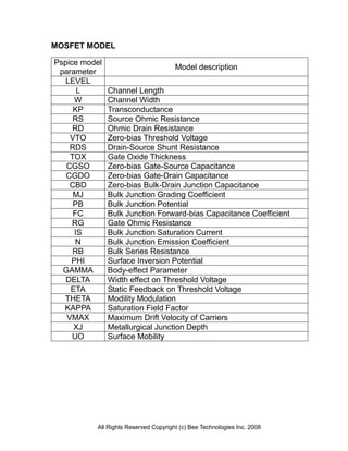
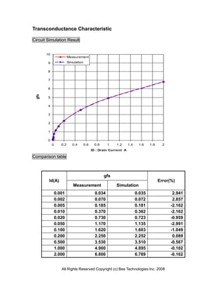
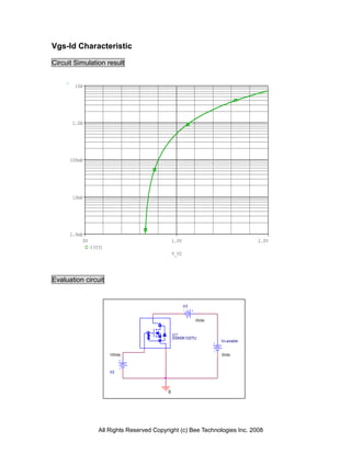
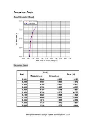
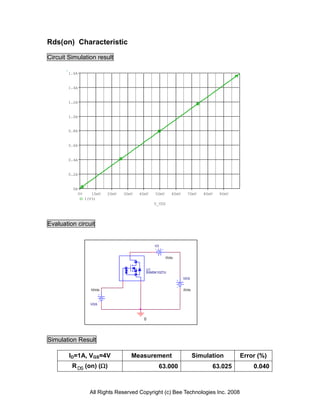
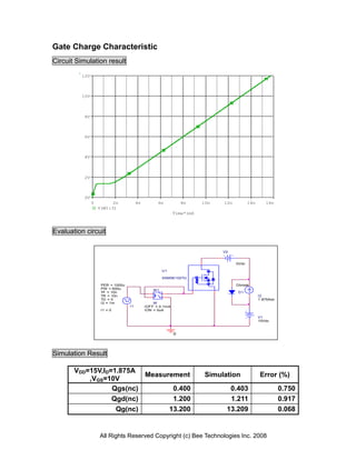
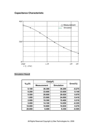

The document is a comprehensive device modeling report for the power MOSFET SSM3K102TU by Toshiba, detailing various electrical characteristics and parameters such as transconductance, gate charge, and capacitance. It includes both measurement and simulation results with error analysis across several metrics, illustrating the performance of the MOSFET in different scenarios. The document outlines the configuration and results of circuit simulations validating the MOSFET's specifications and behavior.


![5G Explained! A High Level Overview [Introduction]](https://cdn.slidesharecdn.com/ss_thumbnails/5gexplainedahighleveloverview-260119165306-cc137a3e-thumbnail.jpg?width=640&height=640&fit=bounds)


