This document provides information on an optocoupler product called the SFH6916. It includes:
- A description of the product as having a GaAs infrared emitter optically coupled to a silicon phototransistor detector in a 16 pin package.
- Features such as high current transfer ratio, isolation voltage, and packaging.
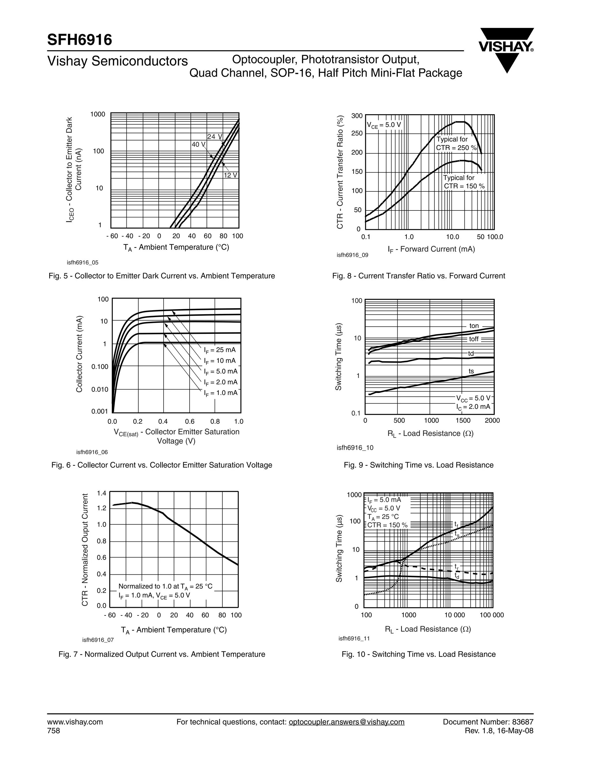
- Electrical characteristics including current ratings, switching times, and current transfer ratio.
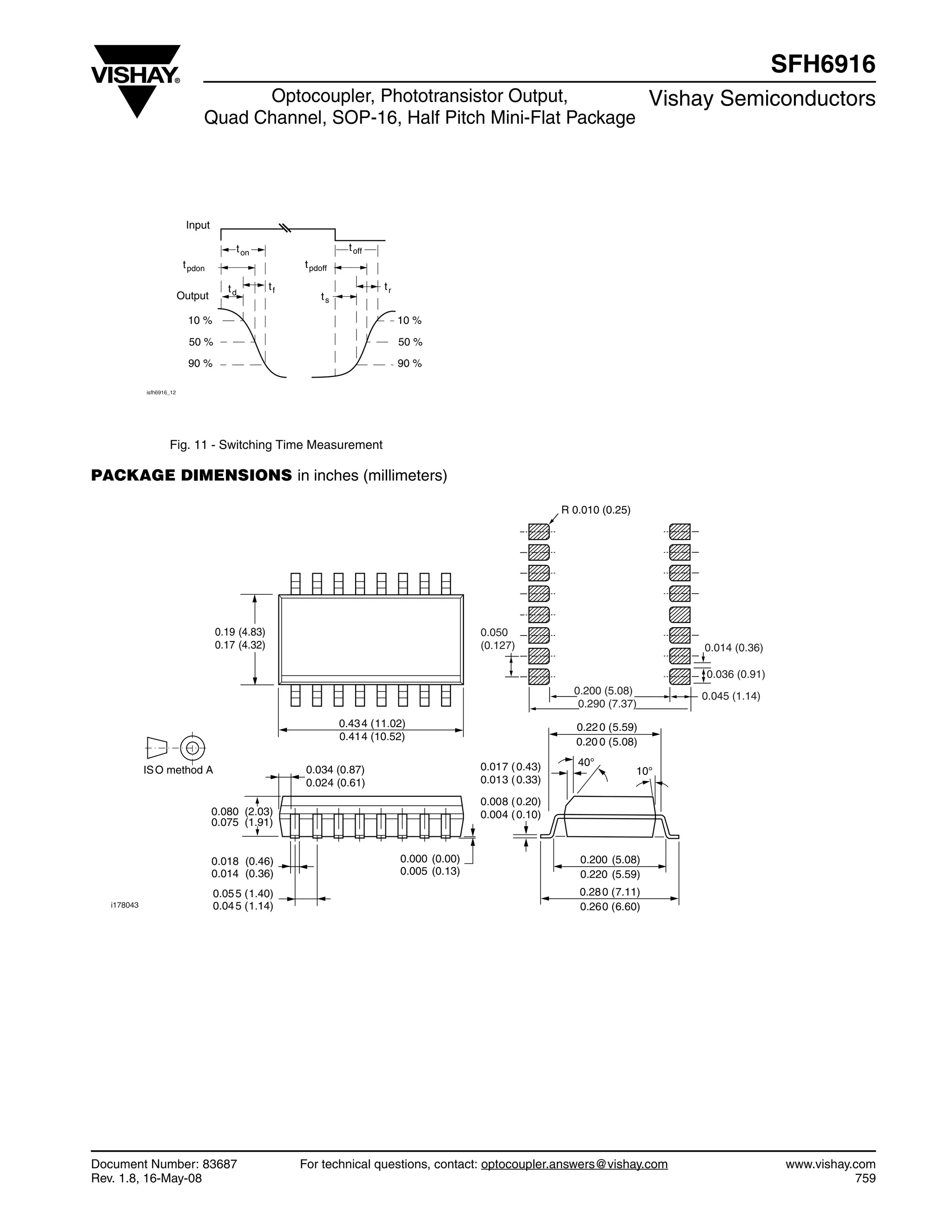
- Packaging dimensions and testing requirements.