WSO2's API Vision: Unifying Control, Empowering Developers
BPV10NF - Datasheet - VISHAY
1. BPV10NF
www.vishay.com
Vishay Semiconductors
Rev. 1.9, 29-May-15 1 Document Number: 81503
For technical questions, contact: detectortechsupport@vishay.com
THIS DOCUMENT IS SUBJECT TO CHANGE WITHOUT NOTICE. THE PRODUCTS DESCRIBED HEREIN AND THIS DOCUMENT
ARE SUBJECT TO SPECIFIC DISCLAIMERS, SET FORTH AT www.vishay.com/doc?91000
Silicon PIN Photodiode
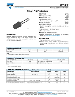
DESCRIPTION
BPV10NF is a PIN photodiode with high speed and high
radiant sensitivity in black, T-1¾ plastic package with
daylight blocking filter. Filter bandwidth is matched with
870 nm to 950 nm IR emitters.
FEATURES
• Package type: leaded
• Package form: T-1¾
• Dimensions (in mm): Ø 5
• Radiant sensitive area (in mm2): 0.78
• Leads with stand-off
• High radiant sensitivity
• Daylight blocking filter matched with 870 nm to 950 nm
emitters
• High bandwidth: > 100 MHz at VR = 12 V
• Fast response times
• Angle of half sensitivity: = ± 20°
• Material categorization: for definitions of compliance
please see www.vishay.com/doc?99912
APPLICATIONS
• High speed detector for infrared radiation
• Infrared remote control and free air data transmission
systems, e.g. in combination with TSFFxxxx series IR
emitters
Note
• Test condition see table “Basic Characteristics”
Note
• MOQ: minimum order quantity
16140-1
PRODUCT SUMMARY
COMPONENT Ira (μA) (deg) 0.5 (nm)
BPV10NF 60 ± 20 790 to 1050
ORDERING INFORMATION
ORDERING CODE PACKAGING REMARKS PACKAGE FORM
BPV10NF Bulk MOQ: 4000 pcs, 4000 pcs/bulk T-1¾
BPV10NF-CS21 Reel MOQ: 5000 pcs, 1000 pcs/reel T-1¾
ABSOLUTE MAXIMUM RATINGS (Tamb = 25 °C, unless otherwise specified)
PARAMETER TEST CONDITION SYMBOL VALUE UNIT
Reverse voltage VR 60 V
Power dissipation Tamb 25 °C PV 215 mW
Junction temperature Tj 100 °C
Operating temperature range Tamb -40 to +100 °C
Storage temperature range Tstg -40 to +100 °C
Soldering temperature t 5 s, 2 mm from body Tsd 260 °C
Thermal resistance junction / ambient Connected with Cu wire, 0.14 mm2 RthJA 350 K/W
2. BPV10NF
www.vishay.com
Vishay Semiconductors
Rev. 1.9, 29-May-15 2 Document Number: 81503
For technical questions, contact: detectortechsupport@vishay.com
THIS DOCUMENT IS SUBJECT TO CHANGE WITHOUT NOTICE. THE PRODUCTS DESCRIBED HEREIN AND THIS DOCUMENT
ARE SUBJECT TO SPECIFIC DISCLAIMERS, SET FORTH AT www.vishay.com/doc?91000
BASIC CHARACTERISTICS (Tamb = 25 °C, unless otherwise specified)
Fig. 1 - Reverse Dark Current vs. Ambient Temperature Fig. 2 - Relative Reverse Light Current vs. Ambient Temperature
BASIC CHARACTERISTICS (Tamb = 25 °C, unless otherwise specified)
PARAMETER TEST CONDITION SYMBOL MIN. TYP. MAX. UNIT
Forward voltage IF = 50 mA VF 1.0 1.3 V
Breakdown voltage IR = 100 μA, E = 0 V(BR) 60 V
Reverse dark current VR = 20 V, E = 0 Iro 1 5 nA
Diode capacitance VR = 0 V, f = 1 MHz, E = 0 CD 11 pF
Open circuit voltage Ee = 1 mW/cm2, = 870 nm VO 450 mV
Short circuit current Ee = 1 mW/cm2, = 870 nm IK 50 μA
Reverse light current
Ee = 1 mW/cm2, = 870 nm, VR = 5 V Ira 55 μA
Ee = 1 mW/cm2, = 950 nm, VR = 5 V Ira 30 60 μA
Temperature coefficient of Ira Ee = 1 mW/cm2, = 870 nm, VR = 5 V TKIra -0.1 %/K
Absolute spectral sensitivity VR = 5 V, = 870 nm s() 0.55 A/W
Angle of half sensitivity ± 20 deg
Wavelength of peak sensitivity p 940 nm
Range of spectral bandwidth 0.5 790 to 1050 nm
Quantum efficiency = 950 nm 70 %
Noise equivalent power VR = 20 V, = 950 nm NEP 3 x 10-14 W/Hz
Detectivity VR = 20 V, = 950 nm D* 3 x 10¹² cmHz/W
Rise time VR = 50 V, RL = 50 , = 820 nm tr 2.5 ns
Fall time VR = 50 V, RL = 50 , = 820 nm tf 2.5 ns
20 40 60 80
1
10
100
1000
Iro
-ReverseDarkCurrent(nA)
Tamb
- Ambient Temperature (°C)
100
94 8436
VR
= 20 V
0 20 40 60 80
0.6
0.8
1.0
1.2
1.4
Irarel
-RelativeReverseLightCurrent
Tamb
- Ambient Temperature (°C)
100
94 8621
VR
= 5 V
Ee
=1 mW/cm2
λ = 870 nm
3. BPV10NF
www.vishay.com
Vishay Semiconductors
Rev. 1.9, 29-May-15 3 Document Number: 81503
For technical questions, contact: detectortechsupport@vishay.com
THIS DOCUMENT IS SUBJECT TO CHANGE WITHOUT NOTICE. THE PRODUCTS DESCRIBED HEREIN AND THIS DOCUMENT
ARE SUBJECT TO SPECIFIC DISCLAIMERS, SET FORTH AT www.vishay.com/doc?91000
Fig. 3 - Reverse Light Current vs. Irradiance
Fig. 4 - Reverse Light Current vs. Reverse Voltage
Fig. 5 - Diode Capacitance vs. Reverse Voltage
Fig. 6 - Relative Spectral Sensitivity vs. Wavelength
Fig. 7 - Relative Radiant Sensitivity vs. Angular Displacement
0.01 0.1 1
0.1
1
10
100
1000
Ira
-ReverseLightCurrent(µA)
Ee
- Irradiance (mW/cm²)
10
94 8622
VR
= 5 V
= 870 nmλ
0.1 1 10
1
10
100
VR
- Reverse Voltage (V)
100
94 8623
Ira
-ReverseLightCurrent(µA)
1 mW/cm2
0.5 mW/cm2
0.2 mW/cm2
0.1 mW/cm2
0.05 mW/cm2
0.02 mW/cm2
λ = 870 nm
0
2
4
6
8
12
10
0.1 1 10
CD
-DiodeCapacitance(pF)
VR
- Reverse Voltage (V)
100
94 8439
E = 0
f = 1 MHz
94 8426
S(λ)rel-RelativeSpectralSensivity
0.0
0.2
0.4
0.6
0.8
1.0
1.2
750 850 950 1050 1150
λ - Wavelength (nm)
0.4 0.2 0
S-RelativeSensitivityrel
94 8624
0.6
0.9
0.8
0°
30°
10° 20°
40°
50°
60°
70°
80°
0.7
1.0
ϕ-AngularDisplacement
4. BPV10NF
www.vishay.com
Vishay Semiconductors
Rev. 1.9, 29-May-15 4 Document Number: 81503
For technical questions, contact: detectortechsupport@vishay.com
THIS DOCUMENT IS SUBJECT TO CHANGE WITHOUT NOTICE. THE PRODUCTS DESCRIBED HEREIN AND THIS DOCUMENT
ARE SUBJECT TO SPECIFIC DISCLAIMERS, SET FORTH AT www.vishay.com/doc?91000
PACKAGE DIMENSIONS in millimeters
96 12198
Drawing-No.: 6.544-5185.01-4