1. CNY70
www.vishay.com
Vishay Semiconductors
Rev. 1.8, 30-Jul-12 1 Document Number: 83751
For technical questions, contact: sensorstechsupport@vishay.com
THIS DOCUMENT IS SUBJECT TO CHANGE WITHOUT NOTICE. THE PRODUCTS DESCRIBED HEREIN AND THIS DOCUMENT
ARE SUBJECT TO SPECIFIC DISCLAIMERS, SET FORTH AT www.vishay.com/doc?91000
Reflective Optical Sensor with Transistor Output
DESCRIPTION
The CNY70 is a reflective sensor that includes an infrared
emitter and phototransistor in a leaded package which
blocks visible light.
FEATURES
• Package type: leaded
• Detector type: phototransistor
• Dimensions (L x W x H in mm): 7 x 7 x 6
• Peak operating distance: < 0.5 mm
• Operating range within > 20 % relative
collector current: 0 mm to 5 mm
• Typical output current under test: IC = 1 mA
• Emitter wavelength: 950 nm
• Daylight blocking filter
• Lead (Pb)-free soldering released
• Material categorization: For definitions of compliance
please see www.vishay.com/doc?99912
APPLICATIONS
• Optoelectronic scanning and switching devices i.e., index
sensing, coded disk scanning etc. (optoelectronic
encoder assemblies).
Notes
(1) CTR: current transfere ratio, Iout/Iin
(2) Conditions like in table basic charactristics/sensors
Note
(1) MOQ: minimum order quantity
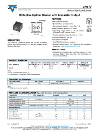
E D
Top view
Marking area
19158_1
21835
PRODUCT SUMMARY
PART NUMBER
DISTANCE FOR
MAXIMUM CTRrel
(1)
(mm)
DISTANCE RANGE FOR
RELATIVE Iout > 20 %
(mm)
TYPICAL OUTPUT
CURRENT UNDER TEST (2)
(mA)
DAYLIGHT
BLOCKING FILTER
INTEGRATED
CNY70 0 0 to 5 1 Yes
ORDERING INFORMATION
ORDERING CODE PACKAGING VOLUME (1) REMARKS
CNY70 Tube MOQ: 4000 pcs, 80 pcs/tube -
ABSOLUTE MAXIMUM RATINGS (Tamb = 25 °C, unless otherwise specified)
PARAMETER TEST CONDITION SYMBOL VALUE UNIT
COUPLER
Total power dissipation Tamb ≤ 25 °C Ptot 200 mW
Ambient temperature range Tamb - 40 to + 85 °C
Storage temperature range Tstg - 40 to + 100 °C
Soldering temperature Distance to case 2 mm, t £ 5 s Tsd 260 °C
INPUT (EMITTER)
Reverse voltage VR 5 V
Forward current IF 50 mA
Forward surge current tp ≤ 10 μs IFSM 3 A
Power dissipation Tamb ≤ 25 °C PV 100 mW
Junction temperature Tj 100 °C
2. CNY70
www.vishay.com
Vishay Semiconductors
Rev. 1.8, 30-Jul-12 2 Document Number: 83751
For technical questions, contact: sensorstechsupport@vishay.com
THIS DOCUMENT IS SUBJECT TO CHANGE WITHOUT NOTICE. THE PRODUCTS DESCRIBED HEREIN AND THIS DOCUMENT
ARE SUBJECT TO SPECIFIC DISCLAIMERS, SET FORTH AT www.vishay.com/doc?91000
ABSOLUTE MAXIMUM RATINGS
Fig. 1 - Power Dissipation vs. Ambient Temperature
Notes
(1) Measured with the “Kodak neutral test card”, white side with 90 % diffuse reflectance
(2) Measured without reflecting medium
OUTPUT (DETECTOR)
Collector emitter voltage VCEO 32 V
Emitter collector voltage VECO 7 V
Collector current IC 50 mA
Power dissipation Tamb ≤ 25 °C PV 100 mW
Junction temperature Tj 100 °C
ABSOLUTE MAXIMUM RATINGS (Tamb = 25 °C, unless otherwise specified)
PARAMETER TEST CONDITION SYMBOL VALUE UNIT
0
100
200
300
0
95 11071
P-PowerDissipation(mW)
Tamb - Ambient Temperature (°C)
IR - diode
Coupled device
Phototransistor
25 50 75 100
BASIC CHARACTERISTICS (Tamb = 25 °C, unless otherwise specified)
PARAMETER TEST CONDITION SYMBOL MIN. TYP. MAX. UNIT
COUPLER
Collector current
VCE = 5 V, IF = 20 mA,
d = 0.3 mm (figure 1)
IC
(2) 0.3 1.0 mA
Cross talk current VCE = 5 V, IF = 20 mA, (figure 2) ICX
(3) 600 nA
Collector emitter saturation
voltage
IF = 20 mA, IC = 0.1 mA,
d = 0.3 mm (figure 1)
VCEsat
(2) 0.3 V
INPUT (EMITTER)
Forward voltage IF = 50 mA VF 1.25 1.6 V
Radiant intensity IF = 50 mA, tp = 20 ms Ie 7.5 mW/sr
Peak wavelength IF = 100 mA λP 940 nm
Virtual source diameter Method: 63 % encircled energy d 1.2 mm
OUTPUT (DETECTOR)
Collector emitter voltage IC = 1 mA VCEO 32 V
Emitter collector voltage IE = 100 μA VECO 5 V
Collector dark current VCE = 20 V, IF = 0 A, E = 0 lx ICEO 200 nA
3. CNY70
www.vishay.com
Vishay Semiconductors
Rev. 1.8, 30-Jul-12 3 Document Number: 83751
For technical questions, contact: sensorstechsupport@vishay.com
THIS DOCUMENT IS SUBJECT TO CHANGE WITHOUT NOTICE. THE PRODUCTS DESCRIBED HEREIN AND THIS DOCUMENT
ARE SUBJECT TO SPECIFIC DISCLAIMERS, SET FORTH AT www.vishay.com/doc?91000
Fig. 2 - Test Condition
BASIC CHARACTERISTICS (Tamb = 25 °C, unless otherwise specified)
Fig. 3 - Forward Current vs. Forward Voltage
Fig. 4 - Relative Current Transfer Ratio vs. Ambient Temperature
Fig. 5 - Collector Current vs. Forward Current
Fig. 6 - Collector Current vs. Collector Emitter Voltage
~~~
~~~
A C E C
Detector
Emitter
d
95 10893
Reflecting medium
(Kodak neutral test card)
0.1
1
10
100
1000
0
VF - Forward Voltage (V)96 11862
IF-ForwardCurrent(mA)
1.61.20.80.4 2.0
0.5
0.6
0.7
0.8
0.9
1.0
1.1
1.2
1.3
1.4
1.5
96 11913
CTR-RelativeCurrentTransferRatiorel
Tamb - Ambient Temperature (°C)
- 30
V = 5 VCE
I = 20 mAF
d = 0.3 mm
50403020100-10- 20 807060
0.1
0.001
0.01
0.1
10
I-CollectorCurrent(mA)C
IF - Forward Current (mA)95 11065
1
Kodak neutral card
(white side)
d = 0.3 mm
VCE = 5 V
100101
VCE - Collector Emitter Voltage (V)95 11066
IF = 50 mA
20 mA
10 mA
5 mA
2 mA
1 mA
0.1
0.001
0.01
0.1
10
I-CollectorCurrent(mA)
C
1
Kodak neutral card
(white side)
d = 0.3 mm
100101
4. CNY70
www.vishay.com
Vishay Semiconductors
Rev. 1.8, 30-Jul-12 4 Document Number: 83751
For technical questions, contact: sensorstechsupport@vishay.com
THIS DOCUMENT IS SUBJECT TO CHANGE WITHOUT NOTICE. THE PRODUCTS DESCRIBED HEREIN AND THIS DOCUMENT
ARE SUBJECT TO SPECIFIC DISCLAIMERS, SET FORTH AT www.vishay.com/doc?91000
Fig. 7 - Current Transfer Ratio vs. Forward Current
Fig. 8 - Current Transfer Ratio vs. Collector Emitter Voltage
Fig. 9 - Collector Current vs. Distance
Fig. 10 - Relative Radiant Intensity/Collector Current vs.
Angular Displacement
Fig. 11 - Relative Collector Current vs. Displacement
0.1
1
10
100
0.1
IF - Forward Current (mA)96 11914
CTR-CurrentTransferRatio(%)
Kodak neutral card
(white side)
d = 0.3 mm
VCE = 5 V
100101
0.1
1
10
VCE - Collector Emitter Voltage (V)96 12001
CTR-CurrentTransferRatio(%)
20 mA
10 mA
5 mA
2 mA
1 mA
IF = 50 mA
Kodak neutral card
(white side)
d = 0.3 mm
0.1 1 10 100
0
0.001
0.1
1
10
I-CollectorCurrent(mA)C
d - Distance (mm)95 11069
VCE = 5 V
IF = 20 mA
d
108642
I-RelativeRadiantIntensityerel
95 11063
0.6
0.9
0.8
0°
30°
10° 20°
40°
50°
60°
70°
80°
0.7
1.0
I-RelativeCollectorCurrentcrel
0.60.40.200.20.4
0.0
0.1
0.2
0.3
0.4
0.5
0.6
0.7
0.8
0.9
1.0
0
s - Displacement (mm)96 11915
VCE = 5 V
IF = 20 mA
I-RelativeCollectorCurrentCrel
d = 5 mm
4 mm
3 mm
2 mm
1 mm
0
E D
D
E
1.5
d
s
0
5 mm
10 mm
s
0
5 mm
10 mm
1110987654321
5. CNY70
www.vishay.com
Vishay Semiconductors
Rev. 1.8, 30-Jul-12 5 Document Number: 83751
For technical questions, contact: sensorstechsupport@vishay.com
THIS DOCUMENT IS SUBJECT TO CHANGE WITHOUT NOTICE. THE PRODUCTS DESCRIBED HEREIN AND THIS DOCUMENT
ARE SUBJECT TO SPECIFIC DISCLAIMERS, SET FORTH AT www.vishay.com/doc?91000
PACKAGE DIMENSIONS in millimeters
TUBE DIMENSIONS in millimeters
95 11345
20291
7. www.vishay.com For technical questions, contact: optocoupleranswers@vishay.com Document Number: 80112
2 Rev. 1.1, 02-Jul-09
Packaging and Ordering Information
Vishay Semiconductors Packaging and Ordering Information
Fig. 2
Fig. 3
15210
15201
8. Document Number: 80112 For technical questions, contact: optocoupleranswers@vishay.com www.vishay.com
Rev. 1.1, 02-Jul-09 3
Packaging and Ordering Information
Packaging and Ordering Information Vishay Semiconductors
Fig. 4
Fig. 5
15199
15202
9. www.vishay.com For technical questions, contact: optocoupleranswers@vishay.com Document Number: 80112
4 Rev. 1.1, 02-Jul-09
Packaging and Ordering Information
Vishay Semiconductors Packaging and Ordering Information
Fig. 6
Fig. 7
15196
15195
10. Document Number: 80112 For technical questions, contact: optocoupleranswers@vishay.com www.vishay.com
Rev. 1.1, 02-Jul-09 5
Packaging and Ordering Information
Packaging and Ordering Information Vishay Semiconductors
Fig. 8
20257
11. Legal Disclaimer Notice
www.vishay.com
Vishay
Revision: 02-Oct-12 1 Document Number: 91000
Disclaimer
ALL PRODUCT, PRODUCT SPECIFICATIONS AND DATA ARE SUBJECT TO CHANGE WITHOUT NOTICE TO IMPROVE
RELIABILITY, FUNCTION OR DESIGN OR OTHERWISE.
Vishay Intertechnology, Inc., its affiliates, agents, and employees, and all persons acting on its or their behalf (collectively,
“Vishay”), disclaim any and all liability for any errors, inaccuracies or incompleteness contained in any datasheet or in any other
disclosure relating to any product.
Vishay makes no warranty, representation or guarantee regarding the suitability of the products for any particular purpose or
the continuing production of any product. To the maximum extent permitted by applicable law, Vishay disclaims (i) any and all
liability arising out of the application or use of any product, (ii) any and all liability, including without limitation special,
consequential or incidental damages, and (iii) any and all implied warranties, including warranties of fitness for particular
purpose, non-infringement and merchantability.
Statements regarding the suitability of products for certain types of applications are based on Vishay’s knowledge of typical
requirements that are often placed on Vishay products in generic applications. Such statements are not binding statements
about the suitability of products for a particular application. It is the customer’s responsibility to validate that a particular
product with the properties described in the product specification is suitable for use in a particular application. Parameters
provided in datasheets and/or specifications may vary in different applications and performance may vary over time. All
operating parameters, including typical parameters, must be validated for each customer application by the customer’s
technical experts. Product specifications do not expand or otherwise modify Vishay’s terms and conditions of purchase,
including but not limited to the warranty expressed therein.
Except as expressly indicated in writing, Vishay products are not designed for use in medical, life-saving, or life-sustaining
applications or for any other application in which the failure of the Vishay product could result in personal injury or death.
Customers using or selling Vishay products not expressly indicated for use in such applications do so at their own risk. Please
contact authorized Vishay personnel to obtain written terms and conditions regarding products designed for such applications.
No license, express or implied, by estoppel or otherwise, to any intellectual property rights is granted by this document or by
any conduct of Vishay. Product names and markings noted herein may be trademarks of their respective owners.
Material Category Policy
Vishay Intertechnology, Inc. hereby certifies that all its products that are identified as RoHS-Compliant fulfill the
definitions and restrictions defined under Directive 2011/65/EU of The European Parliament and of the Council
of June 8, 2011 on the restriction of the use of certain hazardous substances in electrical and electronic equipment
(EEE) - recast, unless otherwise specified as non-compliant.
Please note that some Vishay documentation may still make reference to RoHS Directive 2002/95/EC. We confirm that
all the products identified as being compliant to Directive 2002/95/EC conform to Directive 2011/65/EU.
Vishay Intertechnology, Inc. hereby certifies that all its products that are identified as Halogen-Free follow Halogen-Free
requirements as per JEDEC JS709A standards. Please note that some Vishay documentation may still make reference
to the IEC 61249-2-21 definition. We confirm that all the products identified as being compliant to IEC 61249-2-21
conform to JEDEC JS709A standards.