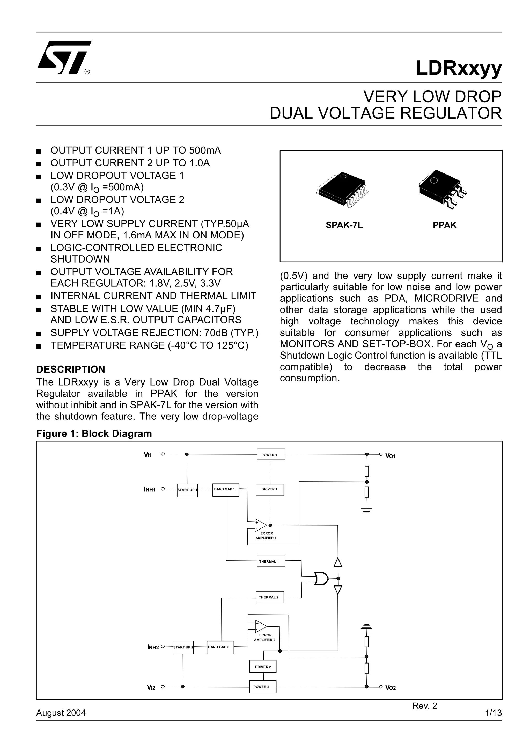
The document describes a dual voltage regulator chip called the LDRxxyy. It has the following key specifications:
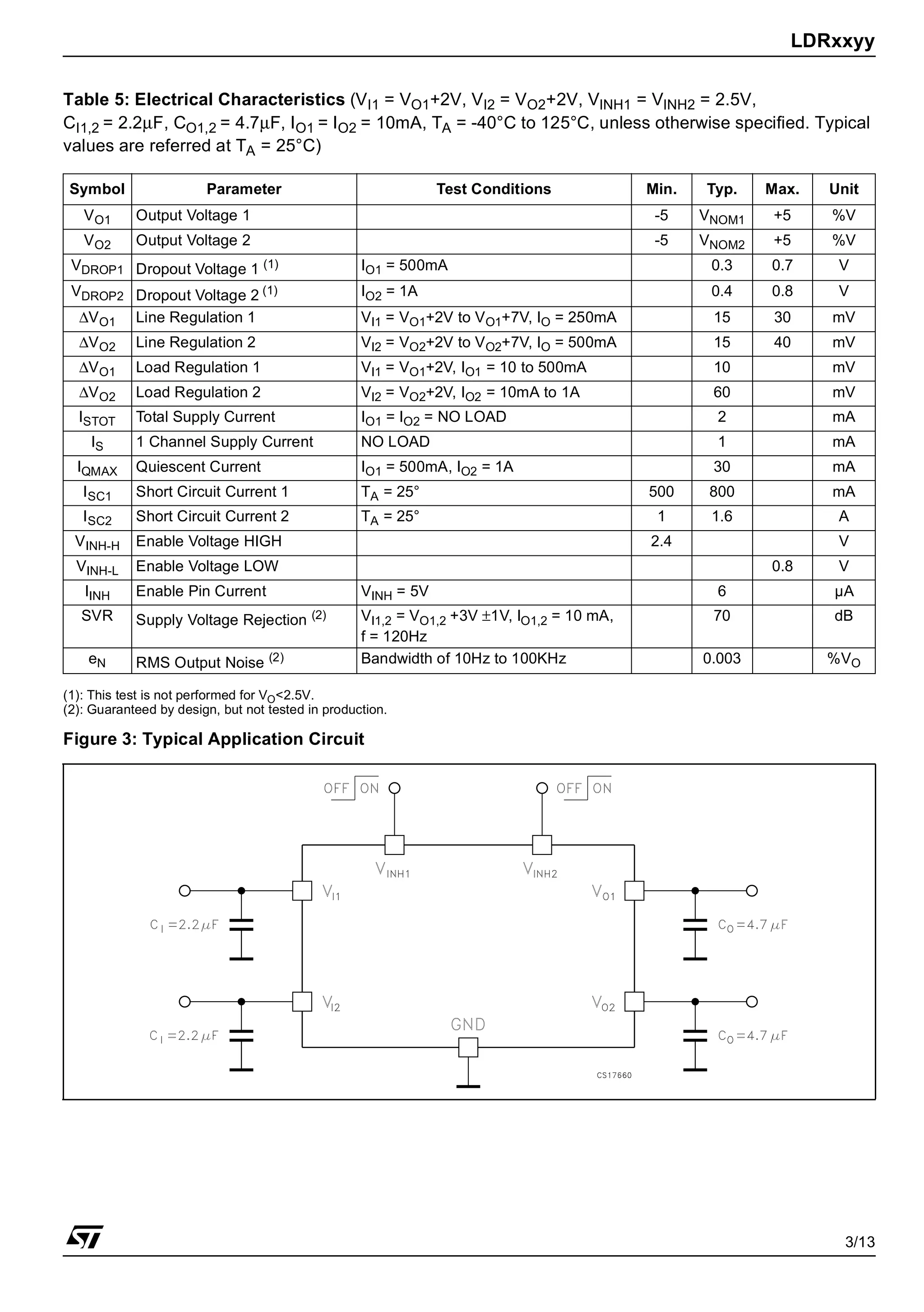
- It provides two independent voltage regulation channels, each able to supply up to 500mA or 1A respectively with low dropout voltages of 0.3V and 0.4V.
- It has very low quiescent current draw of only 50uA in off mode and 1.6mA maximum in on mode.
- Each output voltage channel can be independently enabled or shut down via logic control for low power applications like PDAs and data storage devices.
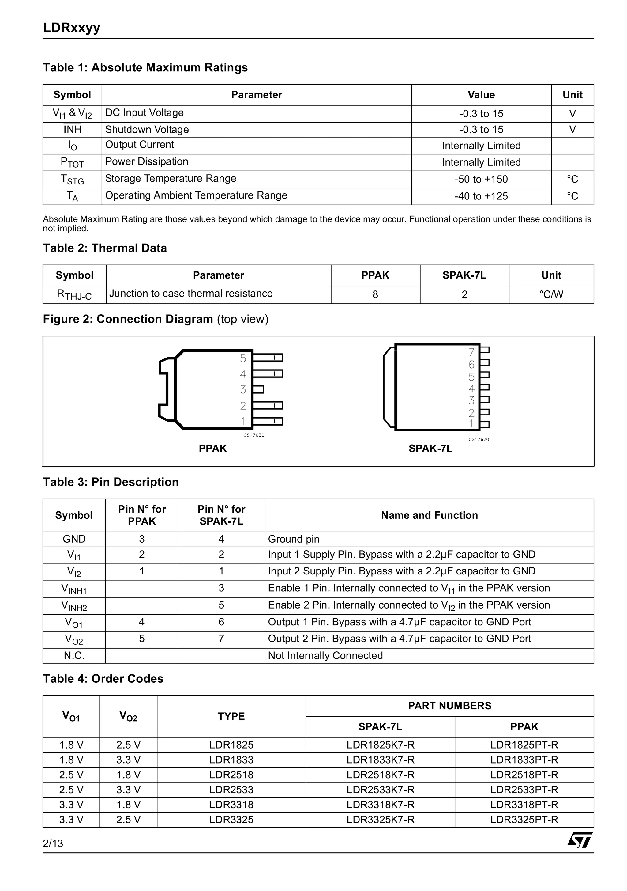
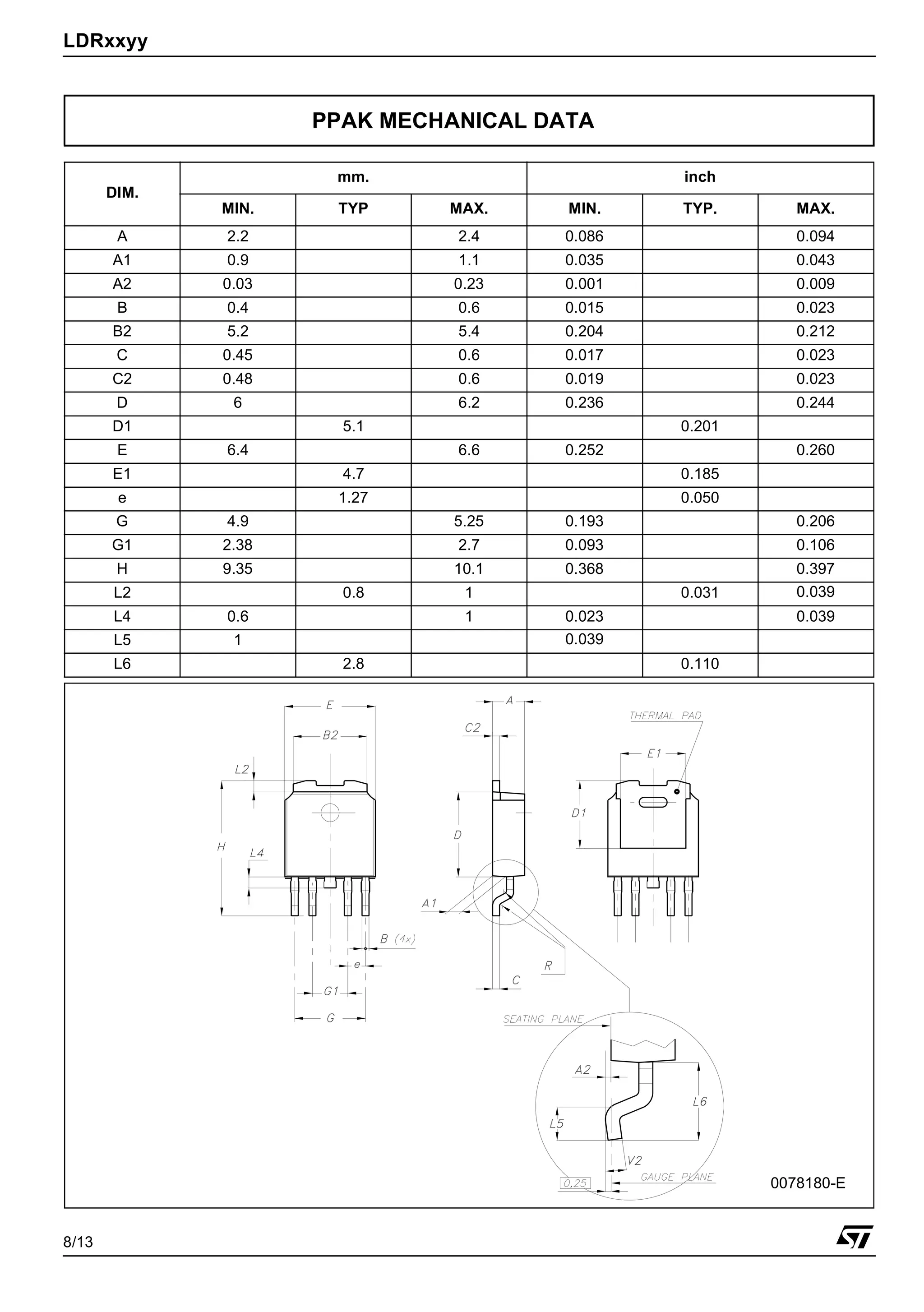
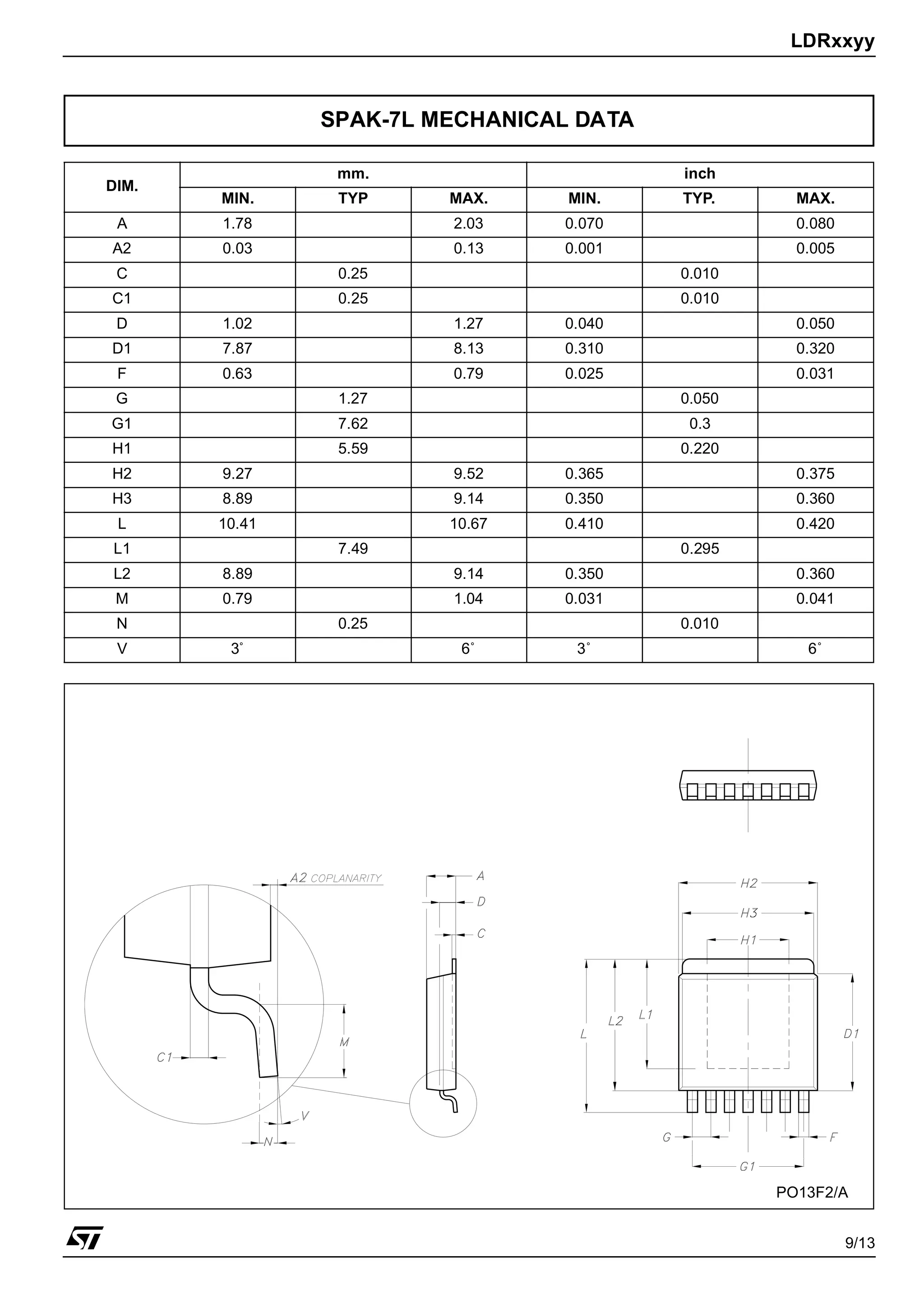
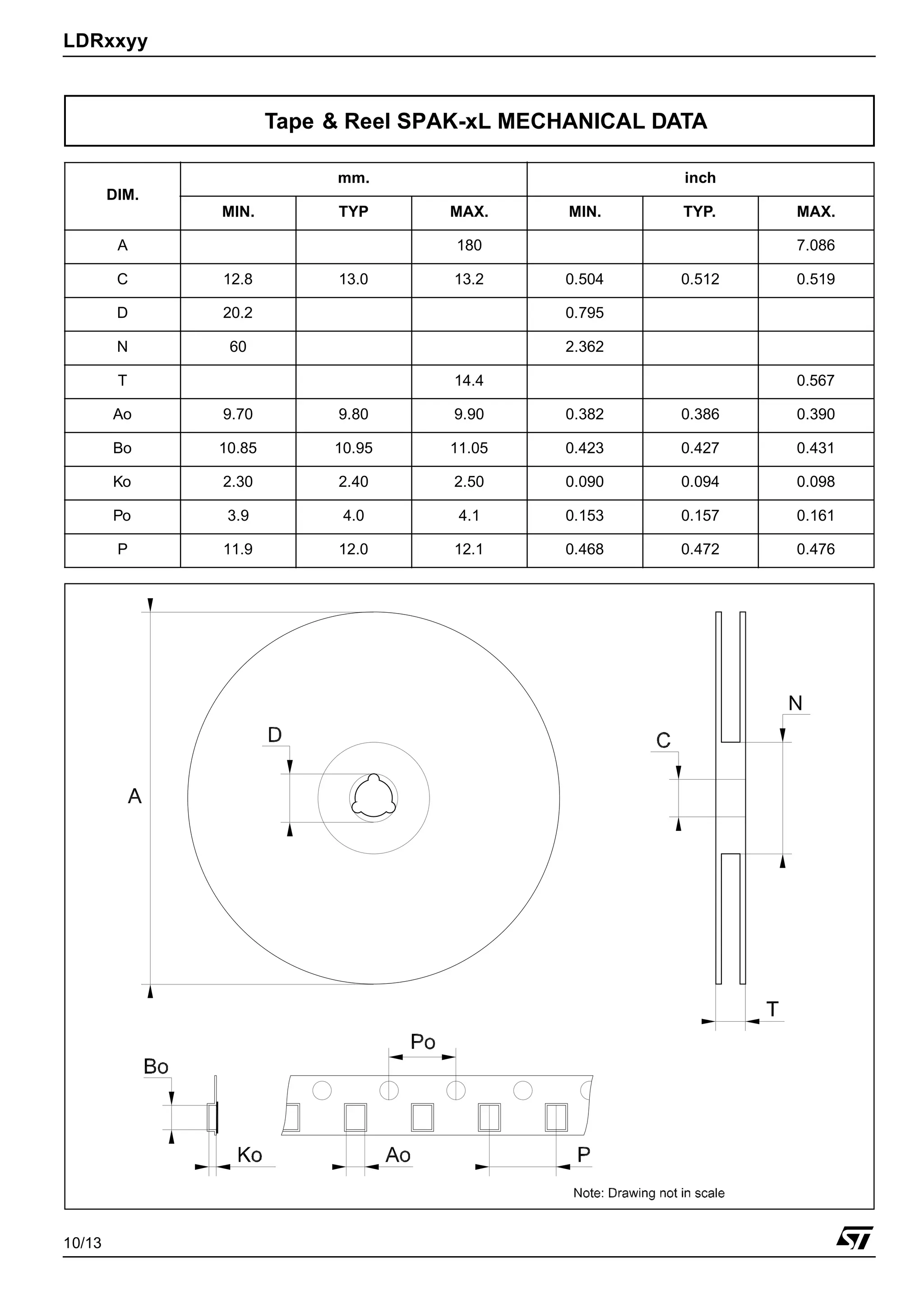
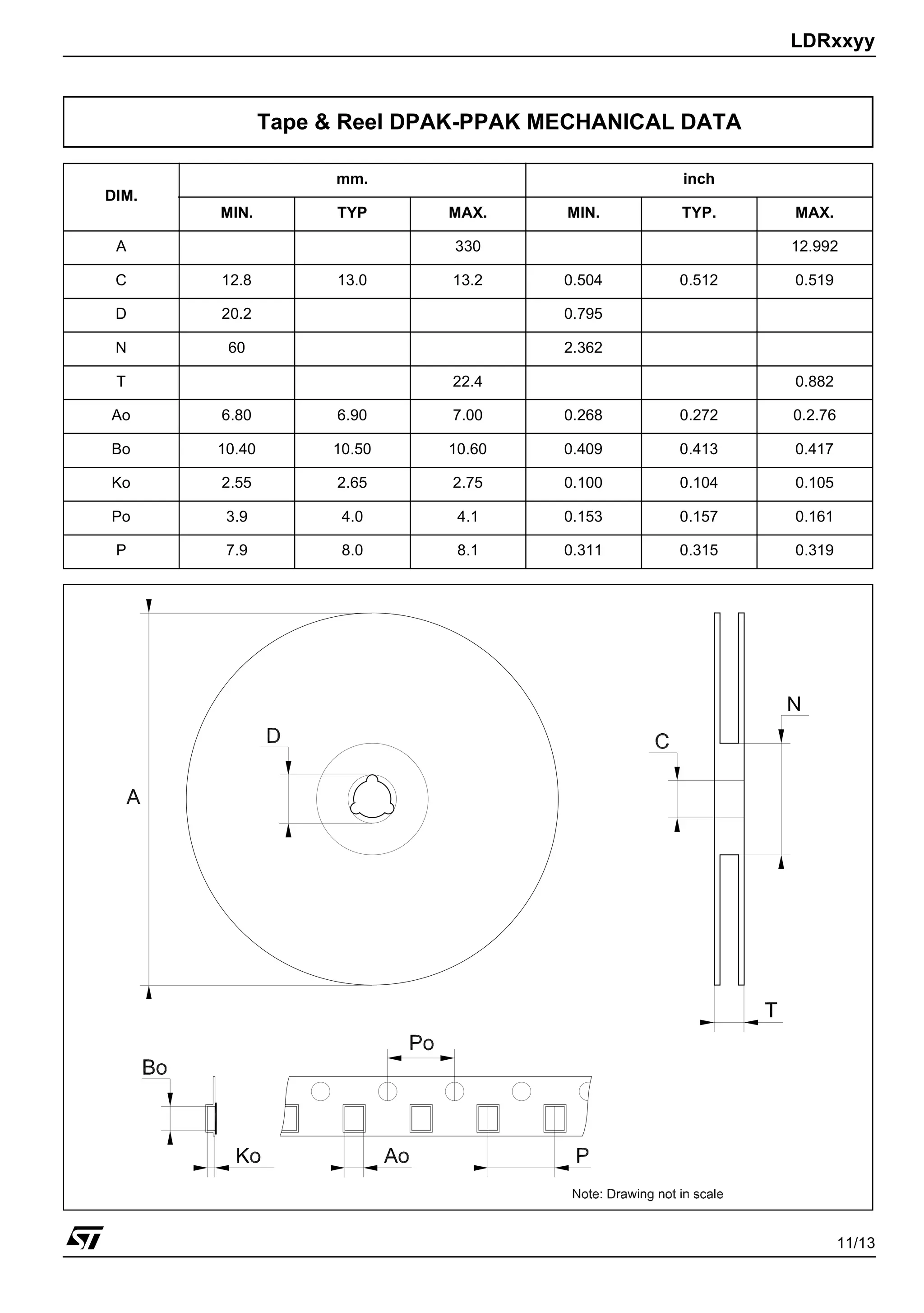
- The chip comes in PPAK and SPAK-7L packages and is suitable for applications from low noise