Download to read offline
![Time
60ms 65ms 70ms 75ms 80ms 85ms 90ms
V(OUT)
9.05V
9.06V
9.07V
9.08V
9.09V
9.10V
SEL>>
Time
89.90ms 89.91ms 89.92ms 89.93ms 89.94ms 89.95ms 89.96ms 89.97ms 89.98ms 89.99ms
V(OUT)
9.060V
9.065V
9.070V
9.075V
9.080V
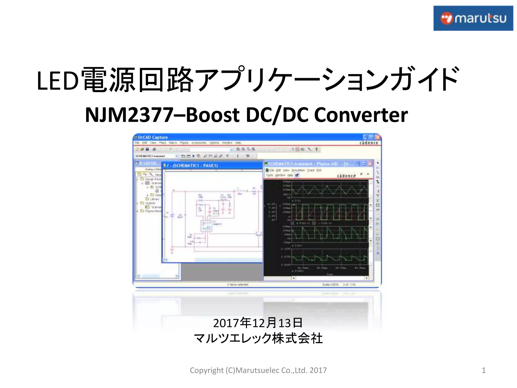
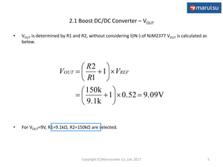
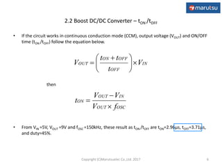
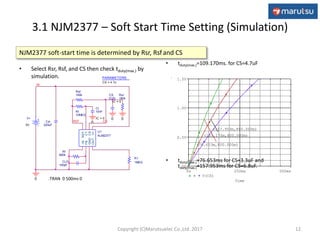
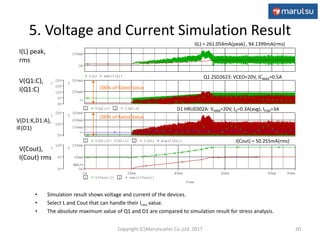
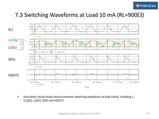
4.2 Output Ripple Voltage
• Simulation result shows output ripple voltage caused by switching(18mVP-P) and
F.B loop oscillation(25mVP-P).
17
V(OUT)
V(OUT)
[ZOOM] 18mVP-P
25mVP-P
Copyright (C)Marutsuelec Co.,Ltd. 2017](https://image.slidesharecdn.com/led-171212055953/85/LED-17-320.jpg)

The document describes the design and operation of a boost DC/DC converter circuit using the NJM2377 control IC. Key aspects covered include: 1) The basic operation of a PWM boost converter and equations for determining output voltage, inductor selection, peak currents, and output capacitor selection. 2) The application circuit configuration using the NJM2377 IC, including settings for soft start time, oscillation frequency, and feedback loop parameters. 3) Simulation results verifying the circuit performance in terms of output voltage, ripple, efficiency and response to load changes.


