This document discusses RF energy harvesting and wireless power transmission for low-power applications. It describes how microwatts of power transmitted over radio waves can be used to trickle charge batteries or power battery-free devices. Key factors that determine the received power are the power of the RF source, distance from the source, size of the receiving antenna, and transmission frequency. Examples of applications that could benefit from this technology include wireless sensors for industrial monitoring and smart buildings.
The document provides an introduction to optoelectronic devices, including their operation and key properties. It discusses:
1) The wave nature of light and how it is described by Maxwell's equations.
2) Polarization and the electromagnetic spectrum, including visible, infrared, and ultraviolet light ranges.
3) Types of optoelectronic devices like p-n junction diodes, heterojunction diodes, laser diodes, photoconductive cells, pin photodiodes, avalanche photodiodes, and photovoltaic cells. It provides details on their principles, structures, and applications.
What is energy harvesting?
What are some of its applications?
Can we make that at home?
#WikiCourses
https://wikicourses.wikispaces.com/XTopic+Energy+Harvesting
“Securing underwater wireless communication networks” 2Naveena N
This document summarizes a seminar presentation on securing underwater wireless communication networks. It discusses the existing challenges with underwater wireless networks including high bit error rates, propagation delays, and low bandwidth. It proposes three schemes for securing such networks: secure time synchronization to enable power saving; secure localization for location information and data tagging; and secure routing to reject paths with malicious nodes. The techniques aim to provide secure data transmission and are based on mechanisms like time synchronization, localization using time/signal information, and routing protocols.
The document provides an introduction to organic electronics research in Henry Yan's group. It discusses three main areas: organic light-emitting diodes (OLEDs) which emit light when a voltage is applied, organic field-effect transistors (OFETs) which are the basic components of flexible electronics, and organic photovoltaics (OPV) which can be produced like printing to provide lightweight solar cells. The research combines chemistry, materials processing, and electrical engineering to develop new organic materials and improve performance of these devices.
This document discusses simulations of carbon nanotube, graphene, and silicon nanowire field effect transistors. It outlines objectives to review nanodevices, simulate different nanodevice structures to study characteristics, and compare results. Sections describe the structures, parameters varied in simulation like dielectric constant and channel length, and results showing the impact on performance metrics like on/off ratio. Future work and conclusions note limitations and potential for further simulation to better optimize device design.
1) The document discusses carrier transport in semiconductors, including drift and diffusion currents. Carrier drift occurs due to an electric field and is characterized by carrier mobility, while diffusion is due to concentration gradients and characterized by the diffusion coefficient.
2) Mobility is affected by phonon and ionized impurity scattering. The net mobility is the sum of these scattering components. Conductivity is directly proportional to carrier concentration and mobility.
3) The Hall effect can be used to determine the type of semiconductor (n-type or p-type), carrier concentration, and carrier mobility. Measurement of the Hall voltage polarity indicates type, and its magnitude relates to concentration and mobility.
1. The document discusses the principles and operation of pn-junction diodes and light emitting diodes (LEDs). It describes how a depletion region forms around the pn-junction due to diffusion of holes and electrons.
2. In an LED, electron-hole pair recombination in the depletion region and surrounding areas results in photon emission. The photon energy is approximately equal to the semiconductor's band gap energy.
3. Common LED materials use direct bandgap III-V semiconductors like GaAs and GaP or their alloys. The bandgap can be tuned to emit light across the visible and infrared spectra. Proper device design and encapsulation helps extract more light from the LED.
The document discusses heterojunctions and p-n junctions. It defines a heterojunction as the interface between two dissimilar semiconductors with different band gaps. There are three types of heterojunctions based on band alignment: type I where bands straddle, type II where bands are staggered, and type III where there is a broken gap. A p-n heterojunction diode forms when a p-doped and n-doped semiconductor meet; electrons flow from the higher to lower Fermi level side and holes in the opposite direction.
This document summarizes a seminar presentation on high-k dielectric devices. It begins by explaining the problems with further scaling silicon dioxide gate dielectrics due to tunneling currents. It then introduces high-k dielectric materials, which have a higher dielectric constant, allowing for thicker dielectric layers with equivalent capacitance. The document discusses issues with compatibility between polysilicon gates and high-k dielectrics, leading to the use of metal gates. It presents the high-k dielectric - metal gate solution adopted by Intel and others, which reduces gate leakage currents and increases performance. Finally, it discusses future opportunities in using high-k dielectrics with non-silicon substrates like germanium.
This document discusses Johnson-Nyquist noise, also known as thermal noise. It is the electronic noise generated by the thermal agitation of charge carriers inside an electrical conductor. The document provides formulas for calculating the noise voltage, power, and current of a resistor based on its temperature and resistance. It also discusses how thermal noise is different from shot noise and examines noise at very high frequencies.
This document provides an overview of organic electronics. It begins with an introduction to organic electronics and conductive organic materials. It then discusses advantages and applications of organic light emitting diodes (OLEDs), organic field effect transistors (OFETs), and organic solar cells (OSCs). The document outlines future uses of organic electronics in areas like transparent devices, printed circuits, smart textiles, and lab-on-a-chip technologies. In conclusion, it states that refinements to organic electronics will lead to numerous everyday applications.
Organic electronics deals with conductive polymers and small molecules for carbon-based electronics. It includes laminar electronics like transparent and paper-based devices. Conductive organic materials can be polymers or small molecules and exhibit electrical conductivity between insulators and metals. Organic light-emitting diodes (OLEDs) have an organic semiconductor layer between electrodes that emits light in response to electric current. Organic electronics have advantages like lower cost fabrication compared to inorganic materials.
This document discusses carbon nanotubes, including their discovery in 1952, types (single-walled and multi-walled), structure, properties, synthesis methods, and potential applications. Carbon nanotubes have extraordinary strength and stiffness, along with high thermal and electrical conductivity. However, they can also be toxic and have crystallographic defects. The three main synthesis methods are arc discharge, laser ablation, and chemical vapor deposition. Carbon nanotubes show promise for applications in materials science, electronics, medicine, and other fields due to their unique properties at the nanoscale.
This document discusses optoelectronic devices and provides examples. It introduces optoelectronics as the study of electronic devices that interact with light. Major optoelectronic devices directly convert between electrons and photons, including light-emitting diodes (LEDs), laser diodes, and photodiodes. LEDs emit light when electrically biased and the color depends on the semiconductor material. Laser diodes use stimulated emission to produce coherent light. Photodiodes are photodetectors that generate a current when struck by photons. The document also discusses solar cells and trends in optoelectronic devices.
This document provides information about circular waveguides. It begins by defining a circular waveguide as a tubular circular conductor that supports TE or TM wave propagation modes. Cutoff wavelengths depend on the internal radius of the waveguide. Common modes for circular waveguides are labeled similarly to rectangular waveguides. The document also provides examples of calculating cutoff wavelengths and wavelengths in a guide for a given signal frequency and waveguide dimensions. It concludes by discussing microstrip and stripline transmission lines used at higher microwave frequencies when waveguides become impractical.
In extrinsic semiconductors, the Fermi level lies close to either the conduction or valence band depending on whether there are more electrons or holes. For n-type semiconductors, donor impurities add extra electrons to the conduction band, making the Fermi level closer to the conduction band. For p-type semiconductors, acceptor impurities create more holes in the valence band, positioning the Fermi level nearer to the valence band. The Fermi level equations show its relation to factors like temperature, carrier concentration, and band properties.
Extreme ultraviolet lithography (EUVL) is an advanced lithography technique needed to continue following Moore's Law and make more powerful microprocessors. EUVL uses light with a wavelength of 13.5nm, which is much shorter than visible light, allowing for smaller feature sizes. The EUVL process involves projecting a mask pattern through a series of reflective mirrors onto a photoresist-coated wafer under vacuum. Key aspects of EUVL include the use of reflective masks and all-reflective optical systems since materials absorb 13.5nm light. EUVL promises increased processor speeds and storage capacity but faces challenges like low mirror reflectivity and contamination control required for the vacuum environment.
This document discusses photonic crystal fibers (PCFs). PCFs are composed of nanostructures that affect photon propagation through periodic refractive indices, similar to how semiconductor crystals affect electron motion. PCFs can guide light through two mechanisms: index guiding and photonic bandgap guiding. They have properties like endless single mode operation, large mode areas, and tunable dispersion. Special PCFs include double core fibers, highly birefringent fibers, and hollow core bandgap fibers. PCFs offer advantages over standard fibers like flexibility in core size and wavelengths used. Challenges include difficult fabrication and limited operating frequencies.
This presentation introduces two-dimensional materials like graphene. It defines two-dimensional materials as being only one or two atoms thick and able to conduct electrons freely within their plane. The document discusses how graphene, being a single layer of graphite, is the strongest material yet and can efficiently conduct heat and electricity. It notes graphene's potential applications in electronics, solar cells, and biomedicine. In conclusion, two-dimensional materials like graphene are seen as having great potential for developing new nanoelectronics, optoelectronics, and flexible devices.
OLED - Organic Light Emitting Diode
Today's most rapidly growing technology in World
All display technology now change to OLED
Less Power consumption
Cost Effective
Flexible
Environment Friendly
Nanoelectronics refers to using nanotechnology in electronic components by controlling and manipulating matter at the nanoscale. This allows the continued miniaturization of electronic devices in accordance with Moore's Law. Some approaches to nanoelectronics include using nanotubes, nanoparticles, single molecule devices, and other nanofabrication techniques. Potential applications include computers, memory storage, displays, and medical devices that take advantage of quantum effects and novel properties at the nanoscale.
This document discusses semiconductors and their types. It defines a semiconductor as a material with conductivity between a metal and an insulator. There are two types of semiconductors - intrinsic and extrinsic. Intrinsic semiconductors are pure, while extrinsic are doped with impurities to be either N-type (excess electrons) or P-type (excess holes). The document explains the carrier concentrations and energy band diagrams of the different semiconductor types.
The document discusses terahertz communication, which uses the terahertz band between 0.3-10 THz for wireless communication. It notes terahertz communication could provide multi-gigabit data rates and help realize applications requiring very high bandwidth. However, challenges include high propagation losses, molecular absorption effects, and short communication ranges. Potential solutions discussed include using ultra-massive MIMO arrays, reconfigurable intelligent surfaces to enhance beamforming gains and extend communication ranges, and distance-aware waveform/modulation designs optimized for terahertz bands.
The document discusses RF energy harvesting, which involves collecting ambient radio frequency energy from sources like TV and cell phone towers to power devices. It describes the concept of using a receiver to collect RF energy and convert it to DC power. The harvesting unit is explained as consisting of an antenna, impedance matching, rectifier to convert RF to DC, and storage components. Different types of antennas and considerations for impedance matching networks are also covered. The document concludes by noting advantages of RF energy harvesting like free wireless power but also challenges of low ambient power levels and conversion efficiency.
Powercast - RF Energy Harvesting for Controllable Wireless Power SystemsHarry Ostaffe
This document discusses RF energy harvesting and wireless power transmission for low-power applications. It describes how microwatts of power transmitted over radio waves can be collected by receiver devices to trickle charge batteries or power devices. Key advantages of this technology include extended battery life, reduced operating costs, and improved product design flexibility. Example applications shown include wireless sensors, RFID tags, and wirelessly charged consumer electronics.
This document describes an elective on energy harvesting that will discuss harnessing renewable energy from the environment, including an overview of energy harvesting, applications, and a hands-on activity where students will characterize solar panels and use the energy to power loads like LEDs, motors, and buzzers. Students will also design a scenario to power a 3 room apartment using solar energy under constraints set by the owner.
These slides use concepts from my (Jeff Funk) course entitled analyzing hi-tech opportunities to show how energy harvesters are becoming more economically feasible for the Internet of Things (IoT). Small amounts of energy can be harvested from vibrations, temperature differences, and radio frequencies using various types of electronic devices such as piezoelectric, MEMS, thermo-electric power generators, and other devices. As improvements in them occur and as the energy requirements of accelerometers, pressure sensors, gas detectors, bio-sensors, and readout circuits fall from microwatts to hundreds of nano-watts, energy harvesters become cheaper and better than are batteries. Improvements in energy harvesting are occurring in the form of higher power per area or higher power per temperature difference and improvements of about five times are expected to occur in the next 5 to 10 years. The market for energy harvesters is expected to reach $2.5 Billion by 2024. In addition to their impact on buildings and the other usual applications for IoT, they will also impact on agriculture, aircraft, and medical implants.
RF Energy Harvesting for Wireless DevicesIJERD Editor
Radio Frequency (RF) energy transfer and harvesting techniques have recently become alternative methods to empower the next generation wireless networks. As this emerging technology enables proactive energy replenishment of wireless devices, it is advantageous in supporting applications with quality of service requirements. In this paper, some wireless power transfer methods, RF energy harvesting networks, various receiver architectures and existing applications are presented. Finally, some open research directions are envisioned.
RF MEMS have potential for energy harvesting by converting electromagnetic energy into electrical charge. The proposed RF MEMS design aims to be scalable and easily integrated in microsystems, unlike existing MEMS energy harvesters that have low efficiency, scaling issues, and high costs. RF MEMS can be fabricated using processes like co-planar waveguide deposition, lithography, aluminum deposition and patterning, and sacrificial layer removal. When activated, the RF MEMS structure can store up to 35 pC of charge per cycle that is generated from the membrane's overlap with the signal isolation layer. However, reliability issues from electrostatic discharge still need to be addressed for practical applications in wireless sensors.
DESIGN & ANALYSIS OF RF ENERGY HARVESTING SYSTEM FOR CHARGING LOW POWER DEVICESJournal For Research
Finite electrical battery life is encouraging the companies and researchers to come up with new ideas and technologies to drive wireless mobile devices for an infinite or enhance period of time. Common resource constrained wireless devices when they run out of battery they should be recharged. For that purpose main supply & charger are needed to charge drained mobile phone batteries or any portable devices. Practically it is not possible to carry charger wherever we go and also to expect availability of power supply everywhere. To avoid such disadvantages some sort of solution should be given and that can be wireless charging of mobile phones.[4] If the mobile can receive RF power signals from the mobile towers, why can’t we extract the power from the received signals? This can be done by the method or technology called RF energy harvesting. RF energy harvesting holds a promise able future for generating a small amount of electrical power to drive partial circuits in wirelessly communicating electronics devices. RF power harvesting is one of the diverse fields where still research continues. The energy of RF waves used by devices can be harvested and used to operate in more effective and efficient way.
Piezoelectric electric based energy harvestingSubash John
Piezoelectric materials can generate an electric charge when subjected to mechanical stress. This phenomenon known as the piezoelectric effect enables piezoelectric materials to convert mechanical vibrational energy into electrical energy through a process known as energy harvesting. Common sources of vibration that can be used for piezoelectric energy harvesting include footsteps on sidewalks, movements from gym equipment, and vibrations from vehicles. The electric energy produced can be stored in batteries or capacitors and used to power small electronic devices. Piezoelectric materials have applications in various technologies including ultrasound imaging, sensors, musical instruments, and automotive engine management systems.
The document describes energy harvesting trees, also known as solar botanic trees. These trees harness renewable energy from the sun, wind, and rain through advanced nano-technologies. The trees consist of nanoleaves, a long tower, LEDs, batteries, and stems connecting the nanoleaves. Nanoleaves generate power from sunlight and wind via the flapping motion, while piezoelectric ribbons in the stems create energy from wind-induced vibrations. Compared to traditional solar panels, these trees require less land for equivalent power generation and provide an efficient, eco-friendly renewable energy solution especially for densely populated areas.
Powercast P2110-EVAL-02 Overview - Lifetime Power® Energy Harvesting Developm...Powercast Corporation
The document describes Powercast's Lifetime Power® Energy Harvesting Development Kit for Battery Charging (P2110-EVAL-02). The kit allows wireless charging of batteries from 40-45 feet away using radio waves. It includes a 3-watt 915MHz transmitter, receiving antennas, a battery charging interface board, a P2110 Powerharvester evaluation board, a THINERGY evaluation card, interface cables, and a TI eZ430-RF2500 wireless kit for demonstrating remote battery charging capabilities. The kit provides a complete solution for developing wirelessly powered systems using RF energy harvesting.
Wireless & Energy Harvesting Technologies for Energy Inefficient BuildingsDan Wright, MBA
This document discusses how energy harvesting and wireless technologies can enable more energy efficient buildings through building automation. It provides an overview of these technologies, including how they work and their benefits. Energy harvesting sensors can power wireless controls without batteries by harvesting small amounts of energy from motion, light, or electromagnetic switching. This allows retrofitting buildings with lighting and HVAC controls to reduce energy use by 20-28% through occupancy-based control. Demonstrations show how energy harvesting switches and sensors communicate wirelessly to automatically control lights.
Development of a wireless sensor network powered by energy harvesting techniquesDaniele Costarella
The document discusses the development of a wireless sensor network powered by energy harvesting techniques. It describes how energy harvesting captures and converts energy from the environment into usable electrical energy. This can power wireless sensor nodes and potentially provide infinite lifetime by replacing batteries. The document outlines various energy sources like solar, thermal, and piezoelectric. It also discusses the design of energy harvesting wireless sensor nodes, including power management circuits, energy storage, sensing, wireless communication, and prototyping challenges. Data analysis of sensor readings and energy levels are demonstrated.
The slides for a presentation on Energy harvesting and the state off the art designs currently taking advantage of the energy around us.
Energy harvesting (also known as power harvesting or energy scavenging) is the process by which energy is derived from external sources (e.g.solar power, thermal energy, wind energy, salinity gradients, and kinetic energy), captured, and stored for small, wireless autonomous devices, like those used in wearable electronics and wireless sensor networks.
Credits: A thanks go out to Johan Pedersen for introducing me to the subject a great workshop and use of some of his slides.
Paul Ahern - Piezoelectric Energy Harvesting ReviewPaul Ahern
Mechanical energy is among the most plentiful and consistent energy sources in our day-to-day lives, which is available to us regardless of the whims of the weather or the cycles of day and night. Piezoelectric Energy Harvesters (PEH’s) are compact devices which allow the scavenging of low grade energy from ambient sources such as human and environmental vibrations, with the aim of using this energy to power autonomous electronic devices. Many decades of research and development in the field has led to commercially available devices based on piezoelectric materials which can be used to harvest milliwatts of energy from mechanical sources such as vibration, stress or strain.
Selection Guide for choosing the best Powerharvester Receiver. The chipset reference design is available for license and supports RF power harvesting of frequencies from 1MHz to 6GHz. Received power is in the range of microwatts (uW) to low milliwatts (mW) depending on the RF input power.
Nano leaves could provide a solution to future energy crises by harnessing solar, thermal, and wind energy through biomimicry of plant leaves. They would consist of nano-photovoltaic, thermoelectric and piezoelectric cells embedded between conductive nano sheets to generate electricity from light, heat and motion like wind. A nano tree producing around 7,000 kWh per year could cost $12,000-$20,000 but last over 20 years, making it cost effective compared to other renewable energy sources. Nano leaves have applications in deserts, parks, and industrial areas to provide green energy and shade.
Passive Wireless Sensor Tags and High-Function RFID tags are enabled by RF Power Harvesting from RFID infrastructure or other dedicated RF power transmitters.
This document discusses batteries and battery chargers for DC and AC backup power systems. It provides an overview of common battery types used in industrial applications, including their typical lifetimes. It also outlines considerations for specifying batteries and chargers, such as load parameters, site conditions that impact battery life, and charger features that can improve battery maintenance and lifespan. The goal is to help ensure batteries perform as expected and last their intended lifetime.
CED CleanLinks Forum Feb. 9, 2012 -- ABB Technology VenturesCEDPrograms
CleanLinks Forums are a partnership between SJF Institute and CED, offering education and practical business advice to cleantech entrepreneurs through moderated discussions, expert panels, and first-person stories from fellow entrepreneurs. Each CleanLinks Forum concludes with a CleanLinks networking reception.
Essential Guide Power Supply & Transformers 2010Gilbert Brault
The document provides information on various power supply and transformer products from Phaseo, including:
- Universal, modular, and dedicated power supplies ranging from 7W to 960W for single or three phase applications.
- Buffer, battery backup, redundancy, and starter protection modules for power supplies.
- Transformers from 25VA to 2500VA for single or three phase use.
This document provides a corporate profile for Power Quality Asia Inc., which has been providing power quality solutions in the Philippines since 1997. It offers services including UPS systems, surge protection, power quality monitoring, and works with major partners for products in these areas. The profile describes Power Quality Asia's mission to be a leader in power quality solutions, lists some of its over 1,300 clients in industries like manufacturing, agriculture, and communications, and provides highlights about its partners' offerings.
This document presents information on engineering DC power plants for telecommunications and data applications. It discusses key considerations such as the equipment to power, required reserve time, voltage operating ranges, plant sizing, distribution architectures, applicable standards, and battery sizing. The presentation provides guidance on single point grounding, voltage drop allowances, rundown problems, and battery disconnects for DC power system design.
Schneider Electric acquired APC in 2007 and merged it with MGE UPS Systems to form its IT Business Unit. The document discusses APC's portfolio of UPS products ranging from 10kVA to 1600kVA, which provide power protection solutions from small wiring closets to large data centers and factories. It also covers APC's scalable modular UPS systems, high efficiency power distribution solutions, power monitoring features, and next generation rack PDU designs.
EPCOS is a leading manufacturer of electronic components and modules that offers power quality solutions. Their broad portfolio includes capacitors, inductors, filters, sensors, and other components. EPCOS focuses on technologically demanding markets like communications, automotive, industrial, and consumer electronics. The document provides an overview of EPCOS' power factor correction product line, including capacitor series, controllers, switching devices, and reactors that can improve power quality by reducing reactive power and improving voltage stability. It also includes fundamentals of power factor correction and component selection guides.
EPCOS is a leading manufacturer of electronic components including capacitors, inductors, EMC filters, sensors and sensor systems, nonlinear resistors, and arresters. It focuses on technologically demanding markets in areas like information technology, automotive, industrial, and consumer electronics. EPCOS offers both standard components and application-specific solutions. It has global design, manufacturing and marketing facilities and is continually improving processes and quality management. EPCOS provides a broad portfolio of power factor correction capacitor series and components for optimizing power quality and factor.
This document discusses challenges in low-power design and verification. It addresses why low-power is now a priority given trends in mobile applications. Key challenges include increased leakage due to process scaling, accounting for active leakage, and handling process variations. The document also discusses low-power design methodologies, including multiple power domains, voltage scaling, and clock gating. Verification challenges are presented, such as needing good test patterns and coordination across design domains. Overall power analysis is more complex than timing analysis due to its pattern dependence and need to optimize for performance per watt.
Here are the key challenges faced in low power design without a common power format:
1. Domain definitions, level shifters, isolation cells, and other low power techniques are specified differently in each tool using tool-specific commands files and languages. This makes cross-tool consistency and validation difficult.
2. Power functionality cannot be easily verified at the RTL level without changing the RTL code, since power domains and low power techniques are not represented. This limits verification coverage.
3. Iteration between design creation and verification is difficult, since changes to the low power implementation require updates to multiple tool-specific specification files rather than a single cross-tool definition. This impacts design schedule and risks inconsistencies.
4.
Atlanta smart grid presentatin 8 30 2011 r3Melanie Brandt
This document discusses electric energy storage technology and applications. It covers drivers for energy storage like increasing renewable penetration, ancillary grid services, and asset management. It provides an overview of the current energy storage landscape and types of technologies. Finally, it discusses US activities to develop storage solutions to help integrate renewables and enhance the grid.
IRJET- Dynamic Wireless Electric Vehicle Charging SystemIRJET Journal
This document summarizes research on a proposed dynamic wireless electric vehicle charging system. It begins with an abstract describing wireless power transfer (WPT) technology and its potential applications for electric vehicle charging. It then provides background on the need for WPT to address limitations of plug-in charging like charging time and battery costs/weight. The document describes various WPT techniques considered for electric vehicle charging and proposes a design using inductive power transfer capable of delivering 15kW of power to a moving vehicle within ±200mm lateral misalignment. It discusses safety considerations for exposure to magnetic fields and concludes that WPT could help accelerate electric vehicle adoption by addressing range and battery concerns.
Presentation from the EPRI-Sandia Symposium on Secure and Resilient Microgrids: IEEE 1547 and Microgrids, presented by Tom Key, EPRI, Baltimore, MD, August 29-31, 2016.
• Solar resource assessment
• Determination of profitability of a PV plant
• Selection and optimization of the site.
• Selection of components (Inverters, Modules, Protection and Wiring, Grounding, Transformers, Metering, Grid Connection)
• Advanced calculations : Estimated losses; Shading study, etc
• Electrical diagrams
The document discusses power quality and network analysis solutions from Alpes Technologies. It describes measuring power quality for utilities, defining power quality, and the interests in monitoring power quality for deregulated markets. It also outlines Alpes Technologies' products for power quality analysis, including permanent and mobile instruments for measuring voltage dips, harmonics, flicker and other parameters.
The document provides information about switchyard protection, powerline carrier communication, and SCADA application in substation control from Power Grid Corporation of India. It includes single line diagrams of substation equipment, descriptions of circuit breakers, lightning arrestors, isolators, and other components. It also explains power line carrier communication using PLCC, and line traps to block carrier waves. Finally, it outlines the architecture and functionality of SCADA systems for data collection, transmission, monitoring, control, and network supervision in power grids.
This document assesses the potential for distributed energy storage in the Australian Capital Territory (ACT). It finds that energy storage could help reduce infrastructure costs by 22% and annual wholesale energy costs by 36% by shifting load. The document also outlines various energy storage technologies and applications, and indicates that energy storage could provide benefits across the supply chain, including for networks, wholesale energy, and reliability. However, it notes that current institutional mechanisms may not fully support accessing multiple revenue streams from different applications and the aggregation of benefits.
This document summarizes a master's thesis presentation on the design of power management for autonomous wireless monitoring systems. It discusses motivation for the work, the state-of-the-art in power management techniques, measurements of RF energy harvesters to characterize performance and derive specifications, design of the power management circuit based on the specifications, and recommendations and conclusions. The work aims to design an efficient power management system that can operate from low power harvested by RF rectennas.
The document discusses blackouts, which refer to a total loss of power to an area. Major blackouts in recent years have affected millions of people. Blackouts can last from minutes to weeks depending on their cause and the electrical network configuration. They are usually caused by a cascade of failures beginning with an initial fault, such as a power plant tripping offline or a transmission line failure overloading other systems. Better monitoring, improved infrastructure like superconducting cables, and a smart grid can help reduce risks of widespread blackouts.
Wattminder provides accurate solar power plant monitoring and diagnostics using data analysis and algorithms. Their software-as-a-service model detects and diagnoses underperformance to help operators maintain optimal performance and revenue. Commercial operators currently lack rigorous monitoring, resulting in poor visibility and unstructured metrics. Wattminder seeks funding to complete product development and begin beta testing.
TimberRock Energy Solutions develops microgrid solutions called Pico-Grids and Multi-Grids that provide energy security, efficiency and reliability while also participating in energy and ancillary services markets. Pico-Grids are autonomous microgrids managed by TimberRock's software to be aggregated into larger Multi-Grids capable of rapidly responding to grid needs. These Multi-Grids generate stronger returns than traditional PPAs by providing additional revenue from ancillary grid services. TimberRock has experience developing and operating commercially financed Pico-Grids and provides hardware and software solutions to empower a smarter electrical grid.
Similar to Powercast Overview - RF Energy Harvesting and Wireless Power for Micro-Power Applications (20)
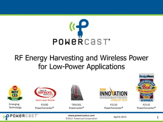
Digital Marketing Trends in 2024 | Guide for Staying AheadWask
https://www.wask.co/ebooks/digital-marketing-trends-in-2024
Feeling lost in the digital marketing whirlwind of 2024? Technology is changing, consumer habits are evolving, and staying ahead of the curve feels like a never-ending pursuit. This e-book is your compass. Dive into actionable insights to handle the complexities of modern marketing. From hyper-personalization to the power of user-generated content, learn how to build long-term relationships with your audience and unlock the secrets to success in the ever-shifting digital landscape.
Letter and Document Automation for Bonterra Impact Management (fka Social Sol...Jeffrey Haguewood
Sidekick Solutions uses Bonterra Impact Management (fka Social Solutions Apricot) and automation solutions to integrate data for business workflows.
We believe integration and automation are essential to user experience and the promise of efficient work through technology. Automation is the critical ingredient to realizing that full vision. We develop integration products and services for Bonterra Case Management software to support the deployment of automations for a variety of use cases.
This video focuses on automated letter generation for Bonterra Impact Management using Google Workspace or Microsoft 365.
Interested in deploying letter generation automations for Bonterra Impact Management? Contact us at sales@sidekicksolutionsllc.com to discuss next steps.
Dive into the realm of operating systems (OS) with Pravash Chandra Das, a seasoned Digital Forensic Analyst, as your guide. 🚀 This comprehensive presentation illuminates the core concepts, types, and evolution of OS, essential for understanding modern computing landscapes.
Beginning with the foundational definition, Das clarifies the pivotal role of OS as system software orchestrating hardware resources, software applications, and user interactions. Through succinct descriptions, he delineates the diverse types of OS, from single-user, single-task environments like early MS-DOS iterations, to multi-user, multi-tasking systems exemplified by modern Linux distributions.
Crucial components like the kernel and shell are dissected, highlighting their indispensable functions in resource management and user interface interaction. Das elucidates how the kernel acts as the central nervous system, orchestrating process scheduling, memory allocation, and device management. Meanwhile, the shell serves as the gateway for user commands, bridging the gap between human input and machine execution. 💻
The narrative then shifts to a captivating exploration of prominent desktop OSs, Windows, macOS, and Linux. Windows, with its globally ubiquitous presence and user-friendly interface, emerges as a cornerstone in personal computing history. macOS, lauded for its sleek design and seamless integration with Apple's ecosystem, stands as a beacon of stability and creativity. Linux, an open-source marvel, offers unparalleled flexibility and security, revolutionizing the computing landscape. 🖥️
Moving to the realm of mobile devices, Das unravels the dominance of Android and iOS. Android's open-source ethos fosters a vibrant ecosystem of customization and innovation, while iOS boasts a seamless user experience and robust security infrastructure. Meanwhile, discontinued platforms like Symbian and Palm OS evoke nostalgia for their pioneering roles in the smartphone revolution.
The journey concludes with a reflection on the ever-evolving landscape of OS, underscored by the emergence of real-time operating systems (RTOS) and the persistent quest for innovation and efficiency. As technology continues to shape our world, understanding the foundations and evolution of operating systems remains paramount. Join Pravash Chandra Das on this illuminating journey through the heart of computing. 🌟
Skybuffer SAM4U tool for SAP license adoptionTatiana Kojar
Manage and optimize your license adoption and consumption with SAM4U, an SAP free customer software asset management tool.
SAM4U, an SAP complimentary software asset management tool for customers, delivers a detailed and well-structured overview of license inventory and usage with a user-friendly interface. We offer a hosted, cost-effective, and performance-optimized SAM4U setup in the Skybuffer Cloud environment. You retain ownership of the system and data, while we manage the ABAP 7.58 infrastructure, ensuring fixed Total Cost of Ownership (TCO) and exceptional services through the SAP Fiori interface.
Programming Foundation Models with DSPy - Meetup SlidesZilliz
Prompting language models is hard, while programming language models is easy. In this talk, I will discuss the state-of-the-art framework DSPy for programming foundation models with its powerful optimizers and runtime constraint system.
Ocean lotus Threat actors project by John Sitima 2024 (1).pptxSitimaJohn
Ocean Lotus cyber threat actors represent a sophisticated, persistent, and politically motivated group that poses a significant risk to organizations and individuals in the Southeast Asian region. Their continuous evolution and adaptability underscore the need for robust cybersecurity measures and international cooperation to identify and mitigate the threats posed by such advanced persistent threat groups.
Skybuffer AI: Advanced Conversational and Generative AI Solution on SAP Busin...Tatiana Kojar
Skybuffer AI, built on the robust SAP Business Technology Platform (SAP BTP), is the latest and most advanced version of our AI development, reaffirming our commitment to delivering top-tier AI solutions. Skybuffer AI harnesses all the innovative capabilities of the SAP BTP in the AI domain, from Conversational AI to cutting-edge Generative AI and Retrieval-Augmented Generation (RAG). It also helps SAP customers safeguard their investments into SAP Conversational AI and ensure a seamless, one-click transition to SAP Business AI.
With Skybuffer AI, various AI models can be integrated into a single communication channel such as Microsoft Teams. This integration empowers business users with insights drawn from SAP backend systems, enterprise documents, and the expansive knowledge of Generative AI. And the best part of it is that it is all managed through our intuitive no-code Action Server interface, requiring no extensive coding knowledge and making the advanced AI accessible to more users.
Driving Business Innovation: Latest Generative AI Advancements & Success StorySafe Software
Are you ready to revolutionize how you handle data? Join us for a webinar where we’ll bring you up to speed with the latest advancements in Generative AI technology and discover how leveraging FME with tools from giants like Google Gemini, Amazon, and Microsoft OpenAI can supercharge your workflow efficiency.
During the hour, we’ll take you through:
Guest Speaker Segment with Hannah Barrington: Dive into the world of dynamic real estate marketing with Hannah, the Marketing Manager at Workspace Group. Hear firsthand how their team generates engaging descriptions for thousands of office units by integrating diverse data sources—from PDF floorplans to web pages—using FME transformers, like OpenAIVisionConnector and AnthropicVisionConnector. This use case will show you how GenAI can streamline content creation for marketing across the board.
Ollama Use Case: Learn how Scenario Specialist Dmitri Bagh has utilized Ollama within FME to input data, create custom models, and enhance security protocols. This segment will include demos to illustrate the full capabilities of FME in AI-driven processes.
Custom AI Models: Discover how to leverage FME to build personalized AI models using your data. Whether it’s populating a model with local data for added security or integrating public AI tools, find out how FME facilitates a versatile and secure approach to AI.
We’ll wrap up with a live Q&A session where you can engage with our experts on your specific use cases, and learn more about optimizing your data workflows with AI.
This webinar is ideal for professionals seeking to harness the power of AI within their data management systems while ensuring high levels of customization and security. Whether you're a novice or an expert, gain actionable insights and strategies to elevate your data processes. Join us to see how FME and AI can revolutionize how you work with data!
Let's Integrate MuleSoft RPA, COMPOSER, APM with AWS IDP along with Slackshyamraj55
Discover the seamless integration of RPA (Robotic Process Automation), COMPOSER, and APM with AWS IDP enhanced with Slack notifications. Explore how these technologies converge to streamline workflows, optimize performance, and ensure secure access, all while leveraging the power of AWS IDP and real-time communication via Slack notifications.
Your One-Stop Shop for Python Success: Top 10 US Python Development Providersakankshawande
Simplify your search for a reliable Python development partner! This list presents the top 10 trusted US providers offering comprehensive Python development services, ensuring your project's success from conception to completion.
Unlock the Future of Search with MongoDB Atlas_ Vector Search Unleashed.pdfMalak Abu Hammad
Discover how MongoDB Atlas and vector search technology can revolutionize your application's search capabilities. This comprehensive presentation covers:
* What is Vector Search?
* Importance and benefits of vector search
* Practical use cases across various industries
* Step-by-step implementation guide
* Live demos with code snippets
* Enhancing LLM capabilities with vector search
* Best practices and optimization strategies
Perfect for developers, AI enthusiasts, and tech leaders. Learn how to leverage MongoDB Atlas to deliver highly relevant, context-aware search results, transforming your data retrieval process. Stay ahead in tech innovation and maximize the potential of your applications.
#MongoDB #VectorSearch #AI #SemanticSearch #TechInnovation #DataScience #LLM #MachineLearning #SearchTechnology
Monitoring and Managing Anomaly Detection on OpenShift.pdfTosin Akinosho
Monitoring and Managing Anomaly Detection on OpenShift
Overview
Dive into the world of anomaly detection on edge devices with our comprehensive hands-on tutorial. This SlideShare presentation will guide you through the entire process, from data collection and model training to edge deployment and real-time monitoring. Perfect for those looking to implement robust anomaly detection systems on resource-constrained IoT/edge devices.
Key Topics Covered
1. Introduction to Anomaly Detection
- Understand the fundamentals of anomaly detection and its importance in identifying unusual behavior or failures in systems.
2. Understanding Edge (IoT)
- Learn about edge computing and IoT, and how they enable real-time data processing and decision-making at the source.
3. What is ArgoCD?
- Discover ArgoCD, a declarative, GitOps continuous delivery tool for Kubernetes, and its role in deploying applications on edge devices.
4. Deployment Using ArgoCD for Edge Devices
- Step-by-step guide on deploying anomaly detection models on edge devices using ArgoCD.
5. Introduction to Apache Kafka and S3
- Explore Apache Kafka for real-time data streaming and Amazon S3 for scalable storage solutions.
6. Viewing Kafka Messages in the Data Lake
- Learn how to view and analyze Kafka messages stored in a data lake for better insights.
7. What is Prometheus?
- Get to know Prometheus, an open-source monitoring and alerting toolkit, and its application in monitoring edge devices.
8. Monitoring Application Metrics with Prometheus
- Detailed instructions on setting up Prometheus to monitor the performance and health of your anomaly detection system.
9. What is Camel K?
- Introduction to Camel K, a lightweight integration framework built on Apache Camel, designed for Kubernetes.
10. Configuring Camel K Integrations for Data Pipelines
- Learn how to configure Camel K for seamless data pipeline integrations in your anomaly detection workflow.
11. What is a Jupyter Notebook?
- Overview of Jupyter Notebooks, an open-source web application for creating and sharing documents with live code, equations, visualizations, and narrative text.
12. Jupyter Notebooks with Code Examples
- Hands-on examples and code snippets in Jupyter Notebooks to help you implement and test anomaly detection models.