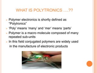
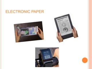
TRANSPARENT ELECTRONICS
Abstract: Transparent electronics is an emerging science and technology field focused on producing ‘invisible’ electronic circuitry and opto-electronic devices.
Applications include consumer electronics, new energy sources, and transportation; for example, automobilewindshields could transmit visual information to the driver. Glass in almost any setting could also double as an electronic device, possibly improving security systems or offering transparent displays. In a similar vein, windows could be used to produce electrical power. Other civilian and military applications in this research field include realtime wearable displays.
As for conventional Si/III–V-based electronics, the basic device structure is based on semiconductor junctions and transistors. However, the device building block materials, the semiconductor, the electric contacts, and the ielectric/passivation layers, must now be transparent in the visible –a true challenge! Therefore, the first scientific goal of this technology must be to discover,understand, and implement transparent high-performance electronic materials. The second goal is their implementation and evaluation in transistor and circuit structures.
The electronics during the past 10 years, the classes of materials available for transparent electronics applications have grown dramatically. Historically, this area was dominated by transparent conducting oxides (oxide materials that are both electrically conductive and optically transparent) because of their wide use in antistatic coatings, touch display panels, solar cells, flat panel displays, heaters, defrosters, ‘smart windows’ and optical coatings. All these applications use transparent conductive oxides as passive electrical or optical coatings. The field of transparent conducting oxide (TCO) materials has been reviewed and many treatises on the topic are available. However, more recently there have been tremendous efforts to develop new active materials for functional transparent electronics. These new technologies will require new materials sets, in addition to the TCO component, including conducting, dielectric and semiconducting materials, as well as passive components for full device fabrication.
COMBINING OPTICAL TRANSPARENCY WITH ELECTRICAL CONDUCTIVITY
Transparent conductors are neither 100% optically transparent nor metallically conductive. From the band structure point of view, the combination of the two properties in the same material is contradictory: a transparent material is an insulator which possesses completely filled valence and empty conduction bands; whereas metallic conductivity appears when the Fermi level lies within a band with a large density of states to provide high carrier concentration. Efficient transparent conductors find their niche in a compromise between a sufficient transmission within the visible spectral range and a moderate but useful in practice electrical conductivity.
E-paper is a revolutionary material that can be used to make next generation electronic displays. It is portable reusable storage and display medium that look like paper but can be repeatedly written one thousands of times. These displays make the beginning of a new area for battery power information applications such as cell phones, pagers, watches and hand-held computers etc.
Like traditional paper, E-paper must be lightweight, flexible, glare free and low cost. Research found that in just few years this technology could replace paper in many situations and leading us ink a truly paperless world.
Semiconductors are materials that have electrical conductivity between conductors such as most metals and nonconductors or insulators like ceramics. How much electricity a semiconductor can conduct depends on the material and its mixture content.
Semiconductors can be insulators at low temperatures and conductors at high temperatures. As they are used in the fabrication of electronic devices, semiconductors play an important role in our lives.
electronics :what is electronics?what are the application of electronics? what is semiconductor?application of semiconductors .why silicon is used more than germanium?
The Roman Empire A Historical Colossus.pdfkaushalkr1407
The Roman Empire, a vast and enduring power, stands as one of history's most remarkable civilizations, leaving an indelible imprint on the world. It emerged from the Roman Republic, transitioning into an imperial powerhouse under the leadership of Augustus Caesar in 27 BCE. This transformation marked the beginning of an era defined by unprecedented territorial expansion, architectural marvels, and profound cultural influence.
The empire's roots lie in the city of Rome, founded, according to legend, by Romulus in 753 BCE. Over centuries, Rome evolved from a small settlement to a formidable republic, characterized by a complex political system with elected officials and checks on power. However, internal strife, class conflicts, and military ambitions paved the way for the end of the Republic. Julius Caesar’s dictatorship and subsequent assassination in 44 BCE created a power vacuum, leading to a civil war. Octavian, later Augustus, emerged victorious, heralding the Roman Empire’s birth.
Under Augustus, the empire experienced the Pax Romana, a 200-year period of relative peace and stability. Augustus reformed the military, established efficient administrative systems, and initiated grand construction projects. The empire's borders expanded, encompassing territories from Britain to Egypt and from Spain to the Euphrates. Roman legions, renowned for their discipline and engineering prowess, secured and maintained these vast territories, building roads, fortifications, and cities that facilitated control and integration.
The Roman Empire’s society was hierarchical, with a rigid class system. At the top were the patricians, wealthy elites who held significant political power. Below them were the plebeians, free citizens with limited political influence, and the vast numbers of slaves who formed the backbone of the economy. The family unit was central, governed by the paterfamilias, the male head who held absolute authority.
Culturally, the Romans were eclectic, absorbing and adapting elements from the civilizations they encountered, particularly the Greeks. Roman art, literature, and philosophy reflected this synthesis, creating a rich cultural tapestry. Latin, the Roman language, became the lingua franca of the Western world, influencing numerous modern languages.
Roman architecture and engineering achievements were monumental. They perfected the arch, vault, and dome, constructing enduring structures like the Colosseum, Pantheon, and aqueducts. These engineering marvels not only showcased Roman ingenuity but also served practical purposes, from public entertainment to water supply.
How to Split Bills in the Odoo 17 POS ModuleCeline George
Bills have a main role in point of sale procedure. It will help to track sales, handling payments and giving receipts to customers. Bill splitting also has an important role in POS. For example, If some friends come together for dinner and if they want to divide the bill then it is possible by POS bill splitting. This slide will show how to split bills in odoo 17 POS.
Instructions for Submissions thorugh G- Classroom.pptxJheel Barad
This presentation provides a briefing on how to upload submissions and documents in Google Classroom. It was prepared as part of an orientation for new Sainik School in-service teacher trainees. As a training officer, my goal is to ensure that you are comfortable and proficient with this essential tool for managing assignments and fostering student engagement.
The French Revolution, which began in 1789, was a period of radical social and political upheaval in France. It marked the decline of absolute monarchies, the rise of secular and democratic republics, and the eventual rise of Napoleon Bonaparte. This revolutionary period is crucial in understanding the transition from feudalism to modernity in Europe.
For more information, visit-www.vavaclasses.com
Model Attribute Check Company Auto PropertyCeline George
In Odoo, the multi-company feature allows you to manage multiple companies within a single Odoo database instance. Each company can have its own configurations while still sharing common resources such as products, customers, and suppliers.
How to Create Map Views in the Odoo 17 ERPCeline George
The map views are useful for providing a geographical representation of data. They allow users to visualize and analyze the data in a more intuitive manner.
We all have good and bad thoughts from time to time and situation to situation. We are bombarded daily with spiraling thoughts(both negative and positive) creating all-consuming feel , making us difficult to manage with associated suffering. Good thoughts are like our Mob Signal (Positive thought) amidst noise(negative thought) in the atmosphere. Negative thoughts like noise outweigh positive thoughts. These thoughts often create unwanted confusion, trouble, stress and frustration in our mind as well as chaos in our physical world. Negative thoughts are also known as “distorted thinking”.
Palestine last event orientationfvgnh .pptxRaedMohamed3
An EFL lesson about the current events in Palestine. It is intended to be for intermediate students who wish to increase their listening skills through a short lesson in power point.
Welcome to TechSoup New Member Orientation and Q&A (May 2024).pdfTechSoup
In this webinar you will learn how your organization can access TechSoup's wide variety of product discount and donation programs. From hardware to software, we'll give you a tour of the tools available to help your nonprofit with productivity, collaboration, financial management, donor tracking, security, and more.
Ethnobotany and Ethnopharmacology:
Ethnobotany in herbal drug evaluation,
Impact of Ethnobotany in traditional medicine,
New development in herbals,
Bio-prospecting tools for drug discovery,
Role of Ethnopharmacology in drug evaluation,
Reverse Pharmacology.
2. BACKGROUND OF ELECTRONICS….
With the invention of transistors in early half of
19th century, the field of electronics has
undergone innumerable changes
Entire concept of electronics is
based on semi-conductors
Silicon is such most widely used
material in manufacture of
electronic circuits
3. DISADVANTAGES BY USAGE OF SILICON….
Production of silicon embedded circuits involves
a huge investment
These circuits also consume more power
Silicon chips are not flexible
Products made by use of silicon
are not portable
This has led to the emergence
of “Polytronics”
4. WHAT IS POLYTRONICS ….??
Polymer electronics is shortly defined as
“Polytronics”
‘Poly’ means ‘many’ and ‘mer’ means ‘parts’
Polymer is a macro molecule composed of many
repeated sub-units
In this field conjugated polymers are widely used
in the manufacture of electronic products
5. HOW DOES A POLYMER CONDUCTS ..?
By obeying Ohm’s law
Ohm’s law defines conductivity in polymers as flow
of electrons or ions
The steps involved in conduction are
a) Doping
b) Mobility of electrons
c) Conductivity
6. ADVANTAGES…..
Freedom in design
Cost effective
Environment friendly
Compact portable products
Consumes less power
Increased picture quality in display devices
Recycled and reused
Light in weight and small