Recommended
PPTX
PN_Junction_FullContent_Professional.pptx
PPTX
PN_Junction_Diode_applied Physics for engineers
PPTX
PN_Junction_Diode_Presentation applied physics .pptx
PPTX
BEEE-Presentation2PN JUNCTION HHQHHD.pptx
PPT
PPTX
PDF
AP LAB PPT.pdf ap lab ppt no title specific
PPTX
2e2c49afc1b0afda8651de988c9cac03.pptx
PPT
pn-junctiondiode-130407041201-phpapp01.ppt
PPT
pn-junctiondiodeJJNINIIJOIOOIMOMOKMOMOIM
PDF
Basic Electronics Semiconductor Diodes
PPTX
PN_Junction_Diode_Amrit_Ghosh_Sainik_School.pptx
PPTX
PPTX
presentationvfvfvfvfvvfvfvfvfvfvvff.pptx
PPTX
Analog electrons introduction
PPTX
pn-junction diode presentation biasing of PN junction
PPTX
PN Junction Diode - VI Characteristics Working
PPTX
PPT-On-PN-Junction-Diode.pptx withits v i
PPTX
PPTX
PPTX
pn-junction-151216100718 (1).pptx
PPT
PDF
The P-N Junction.The P-N Junction.The P-N Junction.The P-N Junction.The P-N J...
DOCX
PPTX
PPTX
PPTX
PDF
PDF
Caribbean Examinations Council Literacy and Numeracy Standards
PDF
GIÁO ÁN KẾ HOẠCH BÀI DẠY NĂNG LỰC SỐ MÔN TIẾNG ANH LỚP 10 CẢ NĂM - GLOBAL SUC...
More Related Content
PPTX
PN_Junction_FullContent_Professional.pptx
PPTX
PN_Junction_Diode_applied Physics for engineers
PPTX
PN_Junction_Diode_Presentation applied physics .pptx
PPTX
BEEE-Presentation2PN JUNCTION HHQHHD.pptx
PPT
PPTX
PDF
AP LAB PPT.pdf ap lab ppt no title specific
PPTX
2e2c49afc1b0afda8651de988c9cac03.pptx
Similar to PN_Junction_Professional_Diagrams_FINAL.pptx
PPT
pn-junctiondiode-130407041201-phpapp01.ppt
PPT
pn-junctiondiodeJJNINIIJOIOOIMOMOKMOMOIM
PDF
Basic Electronics Semiconductor Diodes
PPTX
PN_Junction_Diode_Amrit_Ghosh_Sainik_School.pptx
PPTX
PPTX
presentationvfvfvfvfvvfvfvfvfvfvvff.pptx
PPTX
Analog electrons introduction
PPTX
pn-junction diode presentation biasing of PN junction
PPTX
PN Junction Diode - VI Characteristics Working
PPTX
PPT-On-PN-Junction-Diode.pptx withits v i
PPTX
PPTX
PPTX
pn-junction-151216100718 (1).pptx
PPT
PDF
The P-N Junction.The P-N Junction.The P-N Junction.The P-N Junction.The P-N J...
DOCX
PPTX
PPTX
PPTX
PDF
Recently uploaded
PDF
Caribbean Examinations Council Literacy and Numeracy Standards
PDF
GIÁO ÁN KẾ HOẠCH BÀI DẠY NĂNG LỰC SỐ MÔN TIẾNG ANH LỚP 10 CẢ NĂM - GLOBAL SUC...
PPTX
bundle of care.pptx Priti Bala @ BRD med
PDF
GIÁO ÁN KẾ HOẠCH BÀI DẠY NĂNG LỰC SỐ MÔN TIẾNG ANH LỚP 11 CẢ NĂM - GLOBAL SUC...
PPTX
How to Manage Empty Location in Odoo 18 Inventory
DOCX
COMMUNITY HEALTH NURSING OSCE CHECKLIST.docx
PDF
Agents in Artificial Intelligence: Types, Architecture and Real-World Examples
PDF
McDowell Technical Community College Early Childhood Program Equitable Workfo...
PPTX
ANTISEPTICS AND DISINFECTANTS CHAPTER NO.05.pptx
PPTX
Weaving Threads: Mapping Practitioner Theses to Understand Professional Becom...
PPTX
STERILITY INDICATOR Pharmaceutical microbiology
PPTX
How to Create SMS Marketing Campaigns in Odoo 18
PPTX
How to Manage Product Types in Odoo 18 Sales
PDF
NCA New Family Orientation 2026 Dosemagen.pdf
PPTX
Statistical Data Analysis using R Programming.pptx
PPTX
VAGINAL IRRIGATION..................pptx
PPTX
The Creation Pattern Physical Health.pptx
PPTX
Introduction of Carbohydrates - Dr.M.Jothimuniyandi
PPTX
Exploring car engine oil and lubricants purpose and functions
PPTX
INSTRUCTIONAL MATERIALS IN TEACHING SCIENCE.pptx
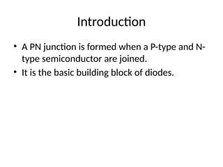
PN_Junction_Professional_Diagrams_FINAL.pptx 1. 2. Introduction
• A PN junction is formed when a P-type and N-
type semiconductor are joined.
• It is the basic building block of diodes.
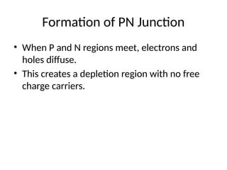
3. 4. 5. Formation of PN Junction
• When P and N regions meet, electrons and
holes diffuse.
• This creates a depletion region with no free
charge carriers.
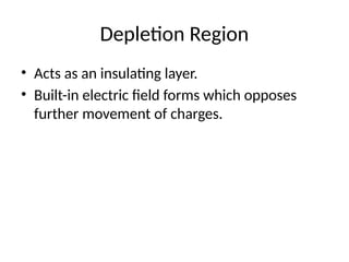
6. Depletion Region
• Acts as an insulating layer.
• Built-in electric field forms which opposes
further movement of charges.
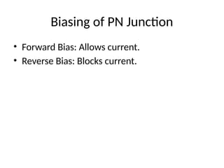
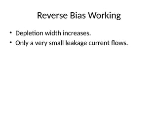
7. Biasing of PN Junction
• Forward Bias: Allows current.
• Reverse Bias: Blocks current.
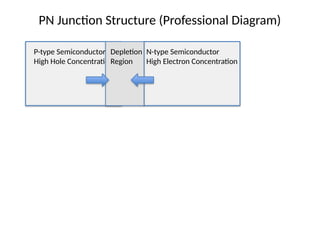
8. 9. 10. 11. PN Junction Structure (Professional Diagram)
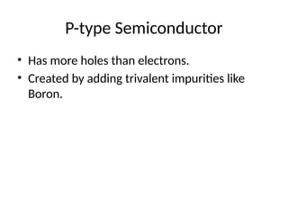
P-type Semiconductor
High Hole Concentration
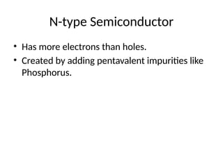
N-type Semiconductor
High Electron Concentration
Depletion
Region
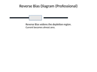
12. Reverse Bias Diagram (Professional)
Reverse Bias widens the depletion region.
Current becomes almost zero.