1) The document is a project report submitted by Sandeep Yadav on building a full wave rectifier circuit under the guidance of his teacher Mr. Vidya Kishore.
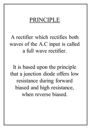
2) A full wave rectifier converts both halves of the alternating current input into pulsating direct current output using a center tapped transformer and two diodes.
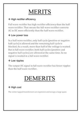
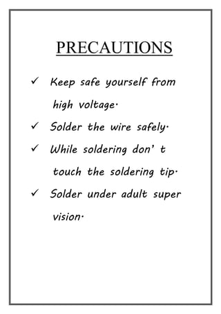
3) The report includes the aim, materials used, working principle, output waveforms, merits like high efficiency and low ripples, and precautions taken during the project.