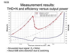
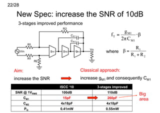
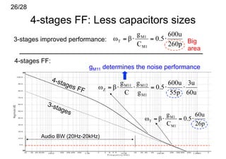
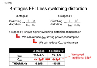
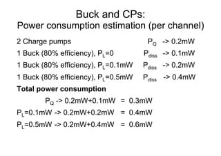
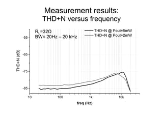
The document details a research project on Class-G headphone amplifiers as part of a Ph.D. thesis at the University of Pavia. It discusses various amplifier classes, focusing on the Class-G architecture, its implementation in 65nm CMOS technology, performance comparisons, and design considerations for improved specifications. The findings indicate that the Class-G amplifier demonstrates lower power consumption and meets stringent market requirements for signal-to-noise ratio and total harmonic distortion.


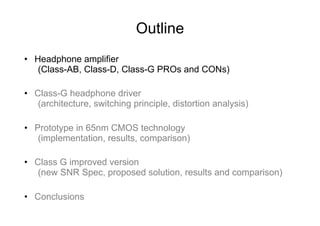


![5/28
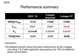
Class G: working principle
VHV
Iout[A] HV stage
Iout[A] iHV LV stage
VLV
iLV iLV
t t
iHV iLV
iHV iLV
Switching
point
-VLV
-VHV
For Vout below the switching point the low voltage stage is active.
For Vout above the switching point both the low voltage and high voltage
stages drive the load (in different moments).](https://image.slidesharecdn.com/lollio10r-12950888036606-phpapp01/85/Phd-3rd-year-Research-Activity-8-320.jpg)


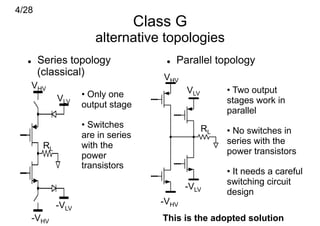
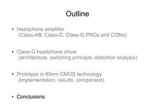
![15/28
Output currents during switching
Vout[V]
VLV • When VOUT is lower than the
VLV -VTH switching point (VLV-VTH) the
switching circuit enables the LV stage
and disables the HV stage
• When VOUT is higher than the low
t voltage supply VLV only the HV stage
Iout[A] drives the load
Output currents
iHV
iLV • When VOUT is between VLV-VTH and
VLV both stages drive the load
t](https://image.slidesharecdn.com/lollio10r-12950888036606-phpapp01/85/Phd-3rd-year-Research-Activity-19-320.jpg)


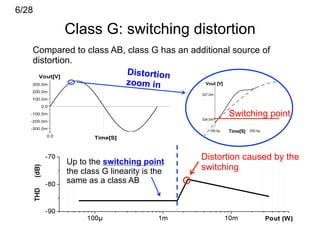
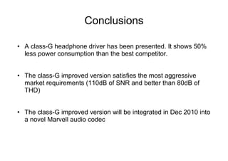
![20/28
Performance summary and
comparison with literature
JSSC 09 ESSCIRC 06 ISCAS 09
This work
Parameter (Class AB) (Class AB) (Class D)
(Class G)
[1] [2] [3]
Technology 65nm 130nm 65nm 0.13um
±1.4V ±1V
Supply voltage 2.5V 3.6V
±0.35V ±0.6V
Quiescent power (per
0.41mW 1.2mW 12.5mW 1.8mW
channel)
Peak load power (16Ω) 90mW 40mW 53.5mW 50mW
-80dB @ -84dB @ -68dB @ -80dB @
THD+N @ PRMS (32Ω)
16mW 10mW 27mW (16Ω) 10mW
92dB (un-
SNR A-weighted 101dB - 96dB
weighted)
[1] Vijay Dhanasekaran, JSCC ‘09 [2] P. Bogner, ESSCIRC ’06
[3] Pillonet, ISCAS ‘09](https://image.slidesharecdn.com/lollio10r-12950888036606-phpapp01/85/Phd-3rd-year-Research-Activity-25-320.jpg)


![References
[1] Vijay Dhanasekaran; Jose Silva-Martinez; Edgar Sanchez-Sinencio, "Design of
Three-Stage Class-AB 16Ohm Headphone Driver Capable of Handling Wide
Range of Load Capacitance," Solid-State Circuits, IEEE Journal of , vol.44, no.6,
pp.1734-1744, Jun 2009.
[2] P. Bogner, H. Habibovic and T. Hartig, ‘‘A High Signal Swing Class AB Earpiece
Amplifier in 65nm CMOS Technology,’’ Proc. ESSCIRC, pp.372-375, 2006.
[3] Pillonet, G., et al,”A 0.01% THD, 70dB PSRR Single Ended Class D using
variable hysteresis control for Headphone Amplifiers”, ISCAS 2009 pp.1181-1184.
[4] Maxim, ‘‘1V, Low-Power, DirectDrive, Stereo Headphone Amplifier with
Shutdown,’’ Rev. 3; 8/08, accessed on Jul. 7, 2009 < http://datasheets.maximic.
com/en/ds/MAX9725.pdf>
[5] Texas Instrument, ‘‘Class-G Directpath Stereo Headphone Amplifier,’’ 3/09,
accessed on Jul. 7, 2009 < http://focus.ti.com/lit/ds/symlink/tpa6141a2.pdf>
[6] National Semiconductor ”Class G Headphone Amplifier with I2C Volume Control,”
August 31,2009, accessed on Jan. 25, 2010
< http://www.national.com/ds/LM/LM48824.pdf >](https://image.slidesharecdn.com/lollio10r-12950888036606-phpapp01/85/Phd-3rd-year-Research-Activity-42-320.jpg)


![July07 4[1].1 power_amplifiers01](https://cdn.slidesharecdn.com/ss_thumbnails/july0741-200727121307-thumbnail.jpg?width=640&height=640&fit=bounds)


