moving message display of lcd
•Download as DOCX, PDF•
2 likes•2,412 views

microcontrolear

Recommended
More Related Content
What's hot
What's hot (20)
Similar to moving message display of lcd
Similar to moving message display of lcd (20)
More from abhishek upadhyay
More from abhishek upadhyay (14)
Recently uploaded
Recently uploaded (20)
moving message display of lcd
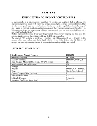
- 1. CHAPTER 1 INTRODUCTION TO PIC MICROCONTROLLERS A microcontroller is a microprocessor which has I/O circuitry and peripherals built-in, allowing it to interface more or less directly with real-world devices such as lights, switches, sensors and motors. They simplify the design of logic and control systems, allowing complex (or simple!) behaviors to be designed into a piece of electronic or electromechanical equipment. They represent an approach which draws on both electronic design and programming skills; an intersection of what was once two disciplines, and is now called “embedded design”. Modern microcontrollers make it very easy to get started. They are very forgiving and often need little external circuitry. Among the most accessible are the PIC microcontrollers. The range of PICs available is very broad – from tiny 6-pin 8-bit devices with just 16 bytes (!) of data memory which can perform only basic digital I/O, to 100-pin 32-bit devices with 512 kilobytes of memory and many integrated peripherals for communications, data acquisition and control. 1 1.1 KEY FEATURES OF PIC16F72 Key Reference Manual Features PIC16F72 Operating Frequency DC-20MHZ RESETS and(delays) POR,BOR,(PWRT,OST) Flash Program Memory(14-bit word,1000 E/W cycles) 2K Data Memory-RAM (8 bit-bytes) 128 Interrupts 8 I/O ports PORTA,PORTB,PORTC Timers Timer0,Timer1,Timer2 Capture/Compare/PWM Modules 1 Serial communications SSP 8-bit A/D Converter 5 channels Instruction Set(No. of instructions) 35
- 2. 2 1.2 Pin configuration 1.3 Block Diagram of PIC16F72 The PIC16F72 belongs to the Mid-Range family of the PIC micro devices. The program memory contains 2K words, which translate to 2048 instructions, since each 14-bit program memory word is the same width as each device instruction. The data memory (RAM) contains 128 bytes. There are 22 I/O pins that are user configurable on a pin-to-pin basis. Some pins are multiplexed with other device functions. These functions include: External interrupt Change on PORTB interrupt Timer0 clock input Timer1 clock/oscillator Capture/Compare/PWM A/D converter SPI/I^2C
- 3. INPUT/OUTPUT PORTS OF PIC16F72 Some pins of the I/O ports are multiplexed with an alternate function for the peripheral features on the device. PORTA and the TRISA Register PORTA is the 6-bit wide, bi-directional port having the data direction register is TRISA. Setting TRISA make the PORTA input port and clearing the TRISA make the PORTA output port. Pin RA4 is multiplexed with the timer0 module clock input to become the RA4/T0CKI pin. The RA4/T0CKI pin is a Schmitt Trigger input and an open drain output. All other RA port pins have TTL input levels and full CMOS output drivers. Name Bit# Buffer Function RA0/AN0 Bit 0 TTL Input/output or analog input RA1/AN1 Bit 1 TTL Input/output or analog input RA2/AN2 Bit 2 TTL Input/output or analog input RA3/AN3/VREF Bit 3 TTL Input/output or analog input or VREF RA4/T0CKI Bit 4 ST Input/output or external clock input for Timer0. Output is open drain type. RA5/AN4/SS Bit5 TTL Input/output or analog input or slave select input for synchronous serial port PORTB and the TRISB Register on a Power-on PORTB is the 8-bit wide, bi-directional port having the data direction register is TRISB. Setting TRISB make the PORTB input port and clearing the TRISB make the PORTB output port. Each of the PORTB pins has a week internal pull-up. A single control bit can turn on all the pull-ups. This is formed by clearing bit RBPU (OPTION<7>). The weak pull-up is automatically turned off when the port pin is configured as an output. The pull-ups are disabled Reset. Name Bit# Buffer Function RB0/INT Bit 0 TTL/ST Input/output pin or external interrupt input. Internal software programmable weak pull-up. RB1 Bit 1 TTL Input/output pin. Internal software programmable weak pull-up. RB2 Bit 2 TTL Input/output pin. Internal software programmable weak pull-up. RB3 Bit 3 TTL Input/output pin. Internal software programmable weak pull-up. RB4 Bit 4 TTLTTL Input/output pin (with interrupt -on-change). Internal software programmable weak pull-up. RB5 Bit 5 TTL Input/output pin (with interrupt -on-change). Internal software programmable weak pull-up. RB6 Bit 6 TTL/ST Input/output pin (with interrupt -on-change). Internal software programmable weak pull-up. Serial programming clock RB7 Bit 7 TTL/ST Input/output pin (with interrupt -on-change). Internal software programmable weak pull-up. Serial programming clock 3
- 4. 4 PORTC and the TRISC Register PORTC is the 8-bit wide, bi-directional port having the data direction register is TRISC. Setting TRISC make the PORTC input port and clearing the TRISC make the PORTC output port. PORTC is multiplexed with various peripheral functions. Name Bit# Buffer type Function RC0/T1OSO/T1CKI Bit 0 ST Input/output port pin or Timer1 oscillator output/Timer1 clock input. RC1/T1OSI Bit 1 ST Input/output port pin or Timer1 oscillator input. RC2/CCP1 Bit 2 ST Input/output port pin or capture1 input/compare1 output/PWM1 output. RC3/SCK/SCL Bit 3 ST RC3 can also be the synchronous serial clock for both SPI and I2C modes. RC4/SDI/SDA Bit 4 ST RC4 can also be the SPI Data. In (SPI mode) or data I/O (I2C mode). RC5/SDO Bit 5 ST Input/output port pin or Synchronous and Serial Port Data output. RC6 Bit 6 ST Input/output port pin. RC7 Bit 7 ST Input/output port pin. 1.4 INTRODUCTION TO TIMERS The timers of the PIC1672 microcontroller can be briefly described in only one sentence. There are three completely independent timers/counters marked as TMR0, TMR1 and TMR2.The three timers are: 1.4.1 Timer TMR0 The timer TMR0 has a wide range of applications in practice. Very few programs don't use it in some way. It is very convenient and easy to use for writing programs or subroutines for generating pulses of arbitrary duration, time measurement or counting external pulses (events) with almost no limitations. The timer TMR0 module is an 8-bit timer/counter with the following features: 8-bit timer/counter; 8-bit prescaler (shared with Watchdog timer); Programmable internal or external clock source;
- 5. Interrupt on overflow and Programmable external clock edge selection The bits which determine the operation of timer0 are stored in the OPTION_REG Register which is given as: 5 RBPU - PORTB Pull-up enable bit o 1 - PORTB pull-up resistors are disabled; and o 0 - PORTB pins can be connected to pull-up resistors. INTEDG - Interrupt Edge Select bit o 1 - Interrupt on rising edge of INT pin (0-1); and o 0 - Interrupt on falling edge of INT pin (1-0). T0CS - TMR0 Clock Select bit o 1 - Pulses are brought to TMR0 timer/counter input through the RA4 pin; and o 0 - Internal cycle clock (Fosc/4). T0SE - TMR0 Source Edge Select bit o 1 - Increment on high-to-low transition on TMR0 pin; and o 0 - Increment on low-to-high transition on TMR0 pin. PSA - Prescaler Assignment bit o 1 - Prescaler is assigned to the WDT; and o 0 - Prescaler is assigned to the TMR0 timer/counter. PS2, PS1, PS0 - Prescaler Rate Select bit o Prescaler rate is adjusted by combining these bits As seen in the table 4-1, the same combination of bits gives different prescaler rate for the timer/counter and watch-dog timer respectively. PS2 PS1 PS0 TMR0 WDT 0 0 0 1:2 1:1 0 0 1 1:4 1:2 0 1 0 1:8 1:4 0 1 1 1:16 1:8 1 0 0 1:32 1:16 1 0 1 1:64 1:32
- 6. 1 1 0 1:128 1:64 1 1 1 1:256 1:128 The logic state of the PSA bit determines whether the prescaler is to be assigned to the timer/counter or watch-dog timer 6 In order to use TMR0 properly, it is necessary: To select mode: Timer mode is selected by the T0CS bit of the OPTION_REG register, (T0CS: 0=timer, 1=counter); When used, the prescaler should be assigned to the timer/counter by clearing the PSA bit of the OPTION_REG register. The prescaler rate is set by using the PS2-PS0 bits of the same register; and When using interrupt, the GIE and TMR0IE bits of the INTCON register should be set. To measure time: Reset the TMR0 register or write some well-known value to it; Elapsed time (in microseconds when using quartz 4MHz) is measured by reading the TMR0 register; and The flag bit TMR0IF of the INTCON register is automatically set every time the TMR0 register overflows. If enabled, an interrupt occurs. To count pulses: The polarity of pulses are to be counted is selected on the RA4 pin are selected by the TOSE bit of the OPTION register (T0SE: 0=positive, 1=negative pulses); and Number of pulses may be read from the TMR0 register. The prescaler and interrupt are used in the same manner as in timer mode. 1.4.2 Timer TMR1 Timer TMR1 module is a 16-bit timer/counter, which means that it consists of two registers (TMR1L and TMR1H). It can count up 65.535 pulses in a single cycle, i.e. before the counting starts from zero.
- 7. Similar to the timer TMR0, these registers can be read or written to at any moment. In case an overflow occurs, an interrupt is generated. The timer TMR1 module may operate in one of two basic modes- as a timer or a counter. However, unlike the timer TMR0, each of these modules has additional functions. Parts of the T1CON register are in control of the operation of the timer TMR1 7 TMR1 in timer mode In order to select this mode, it is necessary to clear the TMR1CS bit. After this, the 16-bit register will be incremented on every pulse coming from the internal oscillator. If the 4MHz quartz crystal is in use, it will be incremented every microsecond. In this mode, the T1SYNC bit does not affect the timer because it counts internal clock pulses. Since the whole electronics uses these pulses, there is no need for synchronization. The microcontroller’s clock oscillator does not run during sleep mode so the timer register overflow cannot cause any interrupt. Timer TMR1 Oscillator The power consumption of the microcontroller is reduced to the lowest level in Sleep mode. The point is to stop the oscillator. Anyway, it is easy to set the timer in this mode- by writing a SLEEP instruction to the program. A problem occurs when it is necessary to wake up the microcontroller because only an interrupt can do that. Since the microcontroller “sleeps”, an interrupt must be triggered by external electronics. It can all get incredibly complicated if it is necessary the ‘wake up’ occurs at regular time intervals... In order to solve this problem, a completely independent Low Power quartz oscillator, able to operate in sleep mode, is built into the PIC16F887 microcontroller. Simply, what previously has been a separate circuit; it is now built into the microcontroller and assigned to the timer TMR1. The oscillator is enabled by setting the T1OSCEN bit of the T1CON register. After that, the TMR1CS bit of the same register then is used to determine that the timer TMR1 uses pulse sequences from that oscillator. The signal from this quartz oscillator is synchronized with the microcontroller clock by clearing the T1SYNC bit. In that case, the timer cannot operate in sleep mode. You wonder why? Because the circuit for synchronization uses the clock of microcontroller!; and The TMR1 register overflow interrupt may be enabled. Such interrupts will occur in sleep mode as well.
- 8. 8 TMR1 in counter mode Timer TMR1 starts to operate as a counter by setting the TMR1CS bit. It means that the timer TMR1 is incremented on the rising edge of the external clock input T1CKI. If control bit T1SYNC of the T1CON register is cleared, the external clock inputs will be synchronized on their way to the TMR1 register. In other words, the timer TMR1 is synchronized to the microcontroller system clock and called a synchronous counter. When the microcontroller, operating in this way, is set in sleep mode, the TMR1H and TMR1L timer registers are not incremented even though clock pulses appear on the input pins. Simply, since the microcontroller system clock does not run in this mode, there are no clock inputs to use for synchronization. However, the prescaler will continue to run if there are clock pulses on the pins since it is just a simple frequency divider. . This counter registers a logic one (1) on input pins. It is important to understand that at least one falling edge must be registered prior to the first increment on rising edge. The arrows in figure denote counter increments.
- 9. T1CON Register U-0 U-0 R/W-0 R/W-0 R/W-0 R/W-0 R/W-0 _______ ______ T1CKPS1 T1CKPS0 T1OSCEN T1SYNC TMR1CS TMR1ON 9 Bit7 bit0 Bit7-6 Unimplemented: Read as ‘0’ Bit 5-4 T1CKPS1:T1CKPS0:Timer1 input clock prescaler select bits 11=1:8 Prescaler value 10=1:4 Prescaler value 01=1:2 Prescaler value 00=1:1 Prescaler value Bit 3 T1OSCEN: Timer1 Oscillator Enable Control bit 1=Oscillator is enabled 0=Oscillator is shut-off (The oscillator inverter is turned off to eliminate power drain) Bit 2 T1SYNC:Timer1 external Clock Input Synchronization Control bit) TMR1CS=1 1=Do not synchronize external clock input 0=Synchronize external clock input Bit1 TMR1CS:Timer1 Clock Source Select bit 1=External clock from pin RC0/T1OSO/T1CKL(on the rising edge 0=internal clock (Fosc/4) Bit 0 TMR1ON:Timer1 on bit 1=Enable timer 0=Stops timer 1.4.3 Timer TMR2 Timer TMR2 module is an 8-bit timer which operates in a very specific way. The pulses from the quartz oscillator first pass through the prescaler whose rate may be changed by combining the T2CKPS1 and T2CKPS0 bits. The output of the prescaler is then used to increment the TMR2 register starting from 00h. The values of TMR2 and PR2 are constantly compared and the TMR2 register keeps on being incremented until it matches the value in PR2. When a match occurs, the TMR2 register is automatically cleared to 00h. The timer TMR2 Postscaler is incremented and its output is used to generate an interrupt if it is enabled. The TMR2 and PR2 registers are both fully readable and writable. Counting may be stopped by clearing the TMR2ON bit, which contributes to power saving. As a special option, the moment of TMR2 reset may be also used to determine synchronous serial communication baud rate.
- 10. The timer TMR2 is controlled by several bits of the T2CON register. TOUTPS3 - TOUTPS0 - Timer2 Output Postcaler Select bits are used to determine the postscaler rate according to the following table: TOUTPS3 TOUTPS2 TOUTPS1 TOUTPS0 POSTSCALER 10 RATE 0 0 0 0 1:1 0 0 0 1 1:2 0 0 1 0 1:3 0 0 1 1 1:4 0 1 0 0 1:5 0 1 0 1 1:6 0 1 1 0 1:7 0 1 1 1 1:8 1 0 0 0 1:9 1 0 0 1 1:10 1 0 1 0 1:11 1 0 1 1 1:12 1 1 0 0 1:13 1 1 0 1 1:14 1 1 1 0 1:15 1 1 1 1 1:16 TMR2ON - Timer2 On bit turns the timer TMR2 on. 1 - Timer T2 is on; and 0 - Timer T2 is off.
- 11. T2CKPS1, T2CKPS0 - Timer2 Clock Prescale bits determine prescaler rate: T2CKPS1 T2CKPS0 PRE SCALER RATE 0 0 1:1 0 1 1:4 1 * 1:16 When using the TMR2 timer, one should know several specific details that have to do with its registers: Upon power-on, the PR2 register contains the value FFh; Both prescaler and postscaler are cleared by writing to the TMR2 register; Both prescaler and postscaler are cleared by writing to the T2CON register; and On any reset, both prescaler and postscaler are cleared. 11 1.5 Capture/Compare/PWM mode: The Capture/Compare/PWM module has three modes of operation: Capture - Capture the time of an event. Compare - Generate an output when Timer 1 reaches a value. PWM - Pulse Width Modulation 1. Capture: Capture mode is used to capture the value of Timer 1 when a signal at the CCP pin goes high (or low depending on how the CCP is set up). The CCP can accurately capture the arrival time of a signal at the CCP pin so it can be used for pulse time measurement 2. Compare: Compare mode is used to generate an output when Timer 1 reaches a value you put into CCPR1. One special event trigger mode lets you start the ADC when the compare mode triggers. 3. PWM: PWM gives you one Pulse Width Modulation output with 5 bit resolution and with no software overhead - once started it operates all by itself unless you want to change the duty cycle. It uses Timer 2 to define its operation using Timer 2 period register to define the frequency of the PWM
- 12. ANALOG-TO –DIGITAL CONVERTER (A/D) MODULE The analog-to-digital (A/D) converter module has five inputs for the PIC16F72. The A/D allows conversion of an analog input signal to a corresponding 8-bit digital number. The output of the sample and hold is the input into the converter, which generates the result via successive approximation. The analog reference voltage is software selectable to either the device’s positive suppIy voltage (VDD) or the voltage level on the RA3/AN3/Vref pin. The A/D converter has a unique feature of being able to operate while the device is in SLEEP mode. To operate in SLEEP, the A/D conversion clock must be derived from the A/D’s internal RC oscillator The A/D module has three registers: • A/D Result Register ADRES • A/D Control Register 0 ADCON0 • A/D Control Register 1 ADCON1 A device RESET forces all registers to their RESET state. This forces the A/D module to be turned off and any conversion is aborted. The ADCON0 register controls the operation of the A/D module. The ADCON1 register configures the functions of the port pins. The port pins can be configured as analog inputs (RA3 can also be a voltage reference) or a digital I/O. ADCON0: A/D CONTROL REGISTER 0 (ADDRESS 1Fh) R/W-0 R/W-0 R/W-0 R/W-0 R/W-0 R/W-0 U-0 R/W-0 ADCS1 ADCS0 CHS2 CHS1 CHS0 GO/DONE ---------- ADON bit 7-6 ADCS<1:0>: A/D Conversion Clock Select bits 00=FOSC/2 01=FOSC/8 10=FOSC/32 11=FRC(clock derived from the internal A/D odule RC oscillator) bit 5-3 CHS<2:0>: Analog Channel Select bits 12 000=channel 0, (RA0/AN0) 001=channel 1, (RA1/AN1) 010=channel 2, (RA2/AN2) 011=channel 3, (RA3/AN3) 100=channel 4, (RA4/AN4) bit 2 GO/DONE: A/D Conversion Status bit If ADON = 1: 1= A/D conversion in progress (setting this bit starts the A/D conversion) 0= A/D conversion not in progress (this bit is automatically cleared by hardware when the A/D conversion is completed ) bit 1 Unimplemented: Read as ‘0’ bit 0 ADON: A/D On bit 1= A/D converter module is operating 0 =A/D converter module is shut-off and consumes no operating current
- 13. ADCON1: A/D CONTROL REGISTER 1 (ADDRESS 9Fh) U-0 U-0 U-0 U-0 U-0 R/W-0 R/W-0 R/W-0 --------- ----------- ----------- ----------- ------------ PCFG2 PCFG1 PCFG0 Bit7-3 unimplemented: read as ‘0’ Bit 2-0 PCFG<2:0>:A/D configuration control bits PCFG2:PCFG0 RA0 RA1 RA2 RA5 RA3 VREF 000 A A A A A VDD 001 A A A A VREF RA3 010 A A A A A VDD 011 A A A A VREF RA3 100 A A D D A VDD 101 A A D D VREF RA3 11X D D D D A VDD 1.6 Special features of PIC16f72 These devices have a host of features intended to maximize system reliability, minimize system reliability, minimize cost through elimination of external components, provide power saving operating modes and offer code protection: Oscillator Selection 13 RESET i. Power-on Reset(POR) ii. Power-up Timer(PWRT) iii. Oscillator Start-up Timer(OST) iv. Brown-out Reset Interrupts Watchdog Timer(WDT) SLEEP Code Protection ID Locations In-Circuit Serial Programming These devices have watchdog timer, which can be enabled or disabled using configuration bits. It run offs its own RC oscillator for added reliability. There are two timers that offer necessary delays on power-up. One is the oscillator start-up timer (OST), intended to keep the chip in RESET until the crystal oscillator is stable. The other is the power-up timer (PWRT), which provides a fixed delay of 72ms (nominal) o n power-up only. It is designed to keep the part in reset while the power supply is stabilizes, and is these are timers on-chip, most applications need no external RESET circuitry. SLEEP mode is designed to offer a very low current Power-down mode. The users can wake-up from SLEEP through external RESET, watchdog Timer wake-up, or through an interrupt.Several oscillator options are also made available to allow the part to fit the application. The RC oscillator option saves system cost while the LP crystal option saves power. Configuration bits are used to select the desired oscillator mode.
- 14. CHAPTER 2 INTERFACINGS OF MOCROCONTROLLERS 14 2.1 INTERFACING WITH LEDS The LED is a two terminal device. We can therefore characterize it according to two quantities: the voltage across it, and the current through it. To a (fairly good) first order, the light output of the LED, either in photons per second or in milli watts, is linearly proportional to the current through it. This means that it is useful to think of the LED as a current-operated device. Here I will be explaining how to interface a LED to a Microcontroller & a sample code for LED flashing. The adjoining figure shows how to interface the LED to 8051 microcontroller. As you can see the Anode is connected through a resistor to Vcc & the Cathode is connected to the Microcontroller pin. So when the Port Pin is HIGH the LED is OFF & when the Port Pin is LOW the LED is turned ON. 8051 has an internal pull-up resistor of 10kΩ. So now when the port Pin is HIGH the Anode is positive with respect to the Cathode so the LED should turn ON right? But the internal pull-up resistor comes in series with the resistor thus limiting the current flowing through the LED. This current is not sufficient enough to Turn ON the LED. Now the block diagram to interface eight led’s with the 8051 is:
- 15. 2.2 INTERFACING WITH SEVEN SEGMENT 7 seg displays are basically 7 LED's. It will be much easier to understand if you first read Interfacing LED's to Microcontroller. Basically there are two types of 7-Seg displays: 1. Common Cathode: where all the segments share the same Cathode. 2. Common Anode: where all Segments share the same Anode. Here we will be only discussing the Common Anode type. In common Anode in order to turn ON a segment the corresponding pin must be set to 0. And to turn it OFF it is set to 1. 15
- 16. Now we create a lookup table containing the seven segment pattern to display the corresponding hex digits. e.g. consider we have to display '1' from the above figure we come to know that turning ON segment B & C will show '1' on the 7-seg display so P2.1 & P2.2 should be LOGIC 0 whereas rest of the pins should be LOGIC 1. The different codes to show the different numbers on the seven segment are given below: 16
- 17. We can now interface a single 7-Seg to the microcontroller but for interfacing multiple 7-seg's we use Scanning Principle where one 7-seg is displayed after another but this process is very fast hence the flickering cannot be seen by human eye. Figure 3 shows the circuit for interfacing two 7 seg displays. When interfacing more than one 7-seg display the segment's (A-G) of all displays are connected together whereas their ANODE (Cathode in case of CC displays) are switched ON one after another. Consider we have to display '31' on the above 7-seg display so we TURN ON the first transistor by setting its corresponding pin to 1 & then give the 7-seg equivalent code for '3' which is 4fh. Then we TURN OFF the first transistor & TURN ON the second & output its corresponding 7-seg equivalent code of '1' i.e. 06h.Then we again go back to display '3' this is a never ending loop. 17
- 18. 18 2.3 INTERFACING WITH LCD 2.3.1 Pin description of LCD: 2.3.2 LCD Initialization: This is the pit fall for beginners. Proper working of LCD depend on the how the LCD is initialized. We have to send few command bytes to initialize the lcd. Simple steps to initialize the LCD 1. Specify function set: Send 38H for 8-bit, double line and 5x7 dot character format. 2. Display On-Off control: Send 0FH for display and blink cursor on. 3. Entry mode set: Send 06H for cursor in increment position and shift is invisible. 4. Clear display: Send 01H to clear display and return cursor to home position.
- 19. 19 2.3.3 Algorithm to send data to LCD: 1. Make R/W low 2. Make RS=0; if data byte is command RS=1; if data byte is data (ASCII value) 3. Place data byte on data register 4. Pulse E (HIGH to LOW) 5. Repeat the steps to send another data byte 2.3.4 Circuit diagram
- 20. CHAPTER 3 PROJECT DESCRIPTION 20 3.1POWER SUPPLY:- 1. Transformer 2. Bridge Rectifier 3. Capacitor 4. Resistance 5. Voltage regulator 6. Led 1. Transformer:- Electrical power transformer is a static device which transforms electrical energy from one circuit to another without any direct electrical connection and with the help of mutual induction between two windings. It transforms power from one circuit to another without changing its frequency but may be in different voltagelevel. 2. Bridge Rectifier:-
- 21. The four diodes labelled D1 to D4 are arranged in “series pairs” with only two diodes conducting current during each half cycle. During the positive half cycle of the supply, diodes D1 and D2conduct in series while diodes D3 and D4 are reverse biased and the current flows through the load. 21 3. Capacitor:- A capacitor (originally known as a condenser) is a passive two-terminal electrical component used to store energyelectrostatically in an electric field. The forms of practical capacitors vary widely, but all contain at least two electrical conductors(plates) separated by a dielectric (i.e. insulator). The conductors can be thin films of metal, aluminum foil or disks, etc. The "nonconducting" dielectric acts to increase the capacitor's charge capacity. A dielectric can be glass, ceramic, plastic film, air, paper, mica, etc. Capacitors are widely used as parts of electrical circuits in many common electrical devices. Unlike a resistor, an ideal capacitor does not dissipate energy. Instead, a capacitor stores energy in the form of an electrostatic field between its plates.
- 22. 22 4. Resistor:- The electrical resistance of a circuit component or device is defined as the ratio of the voltage applied to the electric current which flows through it. If the resistance is constant over a considerable range of voltage, then Ohm's law, I = V/R, can be used to predict the behavior of the material. Although the definition above involves DC current and voltage, the same definition holds for the AC application of resistors. 5. Voltage Regulator:- A voltage regulator is designed to automatically maintain a constant voltage level. A voltage regulator may be a simple "feed-forward" design or may include negative feedback control loops. It may use an electromechanical mechanism, or electronic components. Depending on the design, it may be used to regulate one or more AC or DC voltages. Electronic voltage regulators are found in devices such as computer power supplies where they stabilize the DC voltages used by the processor and other elements. In automobile alternators and central power station generator plants, voltage regulators control the output of the plant. In
- 23. an electric power distribution system, voltage regulators may be installed at a substation or along distribution lines so that all customers receive steady voltage independent of how much power is drawn from the line. 23 6. Led:- A light-emitting diode (LED) is a two-lead semiconductor light source. It is a basic pn-junction diode, which emits light when activated.[7] When a fitting voltage is applied to the leads, electrons are able to recombine with electron holes within the device, releasing energy in the form of photons. This effect is called electroluminescence, and the color of the light (corresponding to the energy of the photon) is determined by the energy band gap of the semiconductor. An LED is often small in area (less than 1 mm2) and integrated optical components may be used to shape its radiation pattern.
- 24. 24 3.2 Power Supply Circuit:- Fig:-Power supply circuit A power supply is an electronic device that supplies electric energy to an electrical load. The primary function of a power supply is to convert one form of electrical energy to another and, as a result, power supplies are sometimes referred to as electric power converters. Some power supplies are discrete, stand-alone devices, whereas others are built into larger devices along with their loads. Examples of the latter include power supplies found in desktop computers and consumer electronics devices. Every power supply must obtain the energy it supplies to its load, as well as any energy it consumes while performing that task, from an energy source. Depending on its design, a power supply may obtain energy from various types of energy sources, including electrical energy transmission systems 1. Crystal Oscillator 2. Pic 16F73 3. LCD Display
- 25. 25 1. Crystal Oscillator :- A crystal oscillator is an electronic oscillator circuit that uses the mechanical resonance of a vibrating crystal of piezoelectric material to create an electrical signal with a very precise frequency.[1][2][3] This frequency is commonly used to keep track of time (as in quartz wristwatches), to provide a stable clock signal for digital integrated circuits, and to stabilize frequencies for radio transmitters and receivers. The most common type of piezoelectric resonator used is the quartz crystal, so oscillator circuits incorporating them became known as crystal oscillators,[1] but other piezoelectric materials including polycrystalline ceramics are used in similar circuits. Quartz crystals are manufactured for frequencies from a few tens of kilohertz to hundreds of megahertz. More than two billion crystals are manufactured annually. Most are used for consumer devices such as wristwatches, clocks, radios, computers, and cellphones. Quartz crystals are also found inside test and measurement equipment, such as counters, signal generators, and oscilloscopes. 2. PIC 16F73 :-
- 26. PIC is a family of modified Harvard architecture microcontrollers made by Microchip Technology, derived from the PIC1650 originally developed by General Instrument's Microelectronics Division. The name PIC initially referred to "Peripheral Interface Controller" now it is "PIC" only. PICs are popular with both industrial developers and hobbyists alike due to their low cost, wide availability, large user base, extensive collection of application notes, availability of low cost or free development tools, and serial programming (and re-programming with flash memory) capability. 26 3. LCD Display:- A liquid crystal display is a special thin flat panel that can let light go through it, or can block the light. (Unlike an LED it does not produce its own light). The panel is made up of several blocks, and each block can be in any shape. Each block is filled with liquid crystals that can be made clear or solid, by changing the electric current to that block. Liquid crystal displays are often abbreviated LCDs. Liquid crystal displays are often used in battery-powered devices, such as digital watches, because they use very little electricity. They are also used for flat screen TV's. Many LCDs work well by themselves when there is other light around (like in a lit room, or outside in daylight). For smartphones, computer monitor, TV's and some other purposes, a back-light is built into the product.
- 27. 3.3 Running Message Display on LCD:- Running-message displays are ideal to get your message (advertisements, greetings, etc) across in an eye-catching way. You can make an LCD show a brief moving message by interfacing it to a microcontroller. Here’s an PIC-based movingmessage display that uses a 16×2 LCD display incorporating HD44780. The 16×2 LCD can display 16 characters per line and there are two such lines. 27 3.4 Circuit description Fig. 1 shows the circuit of the PIC microcontroller- based electronic lock. It can be divided into five sections: input (4×4 matrix keypad), processing unit (PIC16F877A MCU), appliance controller (relay driver), display (16×2 LCD), and power supply. PIC16F877A MCU.The PIC- 16F877A is an 8-bit microcontroller based on reduced instruction set computer (RISC)
- 28. 28
- 29. 29 3.5 PROGRAM: #include <pic.h> #define dataport PORTB #define rs RC5 #define rw RC6 #define en RC7 #define busy RB7 void cmd(unsigned char); void data(unsigned char); void delay(unsigned int); void lcd_ready(); unsigned char a,b,c; unsigned int l,m,n,r,s; unsigned char jjj[]="SATWANT SINGH"; unsigned int kkk; void main() { lcd_ready(); TRISC=0x00;//PORTC output TRISB=0x00;//PORTB output cmd(0x38); cmd(0x01); cmd(0x0c); while(1) { cmd(0x80); kkk=0; while(kkk<13) { data(jjj[kkk]); kkk++; delay(10); } void cmd(unsigned char g) { lcd_ready(); rw=0; rs=0; dataport=g; en=1; delay(10); en=0; }
- 30. 30 void data(unsigned char g) { lcd_ready(); rw=0; rs=1; dataport=g; en=1; delay(10); en=0; } void delay(unsigned int i) { unsigned int h,j; for(h=0;h<i;h++) { for(j=0;j<i;j++); } } void lcd_ready() { TRISB=0x80; rs=0; rw=1; while(busy==1) { en=0; delay(10); en=1; } TRISB=0x00; }
- 31. 31 4.1 Applications Car security system Sensor reporting Automation system Remote Keyless Entry (RKE) Remote Lighting Controls On-Site Paging Asset Tracking Wireless Alarm and Security Systems Long Range RFID Automated Resource Management
- 32. 32 REFRENCE:- [1]: http://en.wikipedia.org/wiki/ [2]: http://www.instructables.com/tag/type-id/category-technology/ [3]: http://electronics.howstuffworks.com/tech [4]: https://www.youtube.com/results?search_query=push+button+telephone [5]:https://www.askanswer.co.in/