The document describes an experiment that used in situ x-ray diffraction to observe the formation of platinum silicide (PtSi) phases when annealing a platinum thin film deposited on silicon. Key findings include:
- PtSi phase formation began around 225°C and halted at 300°C during vacuum annealing, while annealing in air resulted in incomplete reaction due to an amorphous silicon dioxide layer forming.
- The only silicide phases that persisted during heat treatments were PtSi(101) and PtSi(002).
- Thermal expansion measurements found the platinum thin film's coefficient of linear expansion was 1.01 × 10⁻⁵ C−1, close to the bulk value of 9 ×
Invited lecture of the Simposium N "Surface Engineering - functional coatings and modified surfaces" at the XIII SBPMat (Brazilian MRS) meeting, in João Pessoa (Brazil). The lecture took place on September 30th, 2014.
The speaker was Professor Christoph Genzel, from the Helmholtz-Zentrum Berlin für Materialien und Energie (HZB), in Germany, where he heads the Department of Microstructure and Residual Stress Analysis and he coordinates a group of diffraction and scattering. Genzel is also Associate Professor at the Technische Universität Berlin.
Study of columnar growth polycrystalline (sn, cr) co doped in2 o3 films depos...EROMOR
The document describes a study of (Sn, Cr) co-doped In2O3 polycrystalline films deposited by sputtering at different deposition times. X-ray diffraction analysis showed the films were crystalline with the main In2O3 phase present in all samples. Additional Cr3O4 and CrO2 phases were detected in thicker and thinner films respectively. Scanning electron microscopy images revealed the films had a columnar growth structure with good homogeneity. Optical measurements determined an optical band gap of ~3 eV, lower than the expected value of 3.75 eV for bulk In2O3. The films showed a response to acetone gas, indicating potential for gas sensing applications.
Sputtering yield and nanopattern formation study of BNSiO2 (Borosil) at eleva...Dr. Basanta Kumar Parida
Lower sputtering yield of the discharge wall material is a crucial parameter for the performance of Hall Effect Thruster (HET) [1, 2]. In this article, we report the sputtering yield of HET wall
material BNSiO2 (borosil) at elevated temperature ~600 °C using quartz crystal microbalance (QCM). We observe a linear increase in the sputtering yield with temperature and it remains stable during long duration experiments using Xe ions. Two different crystallographic orientations of borosil give a
slight variation in the yield. The higher yields for higher operating temperatures is proposed to be due to the thermal spike nature. Microscopic surface morphology shows only different grains of BNSiO2, however high resolution nanoscopic view reveals the formation of nanoripple like structures over different grains [3]. The periodicity of such features increases with ion dose (sputtering time) and temperature in the range of 70-190 nm. Local curvature dependent erosion plays crucial role in such pattern formation [4].
Reference:
1. D.M. Goebel, I. Katz, Fundamentals of Electric Propulsion, Ion and Hall Thrusters, 2008.
2. M. Ranjan, A. Sharma, A. Vaid, T. Bhatt, V. Nandalan, M.G. James, H. Revathi, S. Mukherjee, AIP
Adv. 6 (2016) 95224
3. R. M. Bradley, J.M.E. Harper, J. Vac. Sci. Technol. A 6 (1988) 2390
4. B. K. Parida, Sooraj K P, S. Hans, V. Pachchigar, S. Augustine, Remyamol T, M. R. Ajith, M. Ranjan;
Nucl. Inst and Methods B, 514 (2022) 1-7
Bismuth ferrite is a multiferroic material with rhombohedral crystal structure and Curie and Neel temperatures of 825°C and 360°C respectively. It exhibits ferroelectricity and ferromagnetism simultaneously. Bismuth ferrite nanoparticles were synthesized using a sol-gel method, which is a bottom-up approach involving hydrolysis and condensation of bismuth nitrate, iron nitrate, and citric acid precursors. The nanoparticles were characterized using X-ray diffraction, which confirmed the hexagonal crystal structure and an average crystalline size of 33.87 nm. Nanoparticle-based technologies are important for developing advanced applications in areas such as memory devices, telecommunications, and
This document summarizes the development of a new composite sensor material made of graphite and epoxy resin. Preliminary studies tested different ratios of graphite and epoxy to find the ideal composition. The 65% graphite composite was found to have suitable properties like stability, moldability and low cost. Further characterization of the 65% composite showed it has low surface roughness and hardness, making it suitable for use as an electroanalytical sensor substrate. Cyclic voltammetry demonstrated the composite has comparable electroactive properties to glassy carbon. The new low-cost composite shows potential for use in electrochemical sensors and cells.
International Journal of Engineering Research and Applications (IJERA) is an open access online peer reviewed international journal that publishes research and review articles in the fields of Computer Science, Neural Networks, Electrical Engineering, Software Engineering, Information Technology, Mechanical Engineering, Chemical Engineering, Plastic Engineering, Food Technology, Textile Engineering, Nano Technology & science, Power Electronics, Electronics & Communication Engineering, Computational mathematics, Image processing, Civil Engineering, Structural Engineering, Environmental Engineering, VLSI Testing & Low Power VLSI Design etc.
The document discusses the development of tribological PVD coatings. It provides examples of materials and processing techniques used to develop such coatings, including pulsed magnetron sputtering and modulated pulse power. It also describes experiments conducted to study the effects of residual stress gradients in PVD TiN coatings on wear resistance, where coatings with varying stress levels were produced and evaluated using scratch and pin-on-disk testing.
Synthesis and charaterization of la1 x srxmno3 perovskite nanoparticlesMai Trần
In recent times perovskite materials are extensively studied and have attracted much attention because they exhibit interesting the properties, showing potential applications in commercial, technical and biomedical. In Vietnam, perovskite materials be of interest research and applications are strong but with major research direction is to go deep into the electrical properties and the magnetic properties. The Lanthanum Strontium manganite is a perovskite-based crystal-structured ceramic material with the formula of La1-xSrxMnO3, where x describes the doping ratio. It has attracted much attention due to its good magnetic, electrical, and catalytic properties and is becoming an attractive possibility material in several biomedical applications, particularly with nano-size. In industry, this material is commonly used in as a cathode material in commercially produced solid oxide fuel cells. In this thesis, we present the Perovskite nanoparticles La1-xSrxMnO3 were successfully synthesized of the nanosize La1-xSrxMnO3 at x = 0; 0.1; 0.2; 0.3 and 0.4 which prepared by a modified sol-gel method. Structure and magnetic properties of them were systematically investigated in dependence on doped Sr ratio x. The structure was investigated by XRD and show slightly changed but magnetic properties varied strongly with changing the doping ratio x. Magnetic properties of samples were studied by Vibrating Sample Mode of Physical Properties Measurement System show at the room temperature, the samples show superparamagnetic properties with high saturated magnetization MS of 57 emu/g which strongly dependents on the doped Sr ratio x.
This document summarizes the synthesis and characterization of thin films of pure TiO2 and Sr-doped TiO2 prepared by spin coating technique. Transparent thin films were prepared on glass substrates and annealed at different temperatures from 3000C to 6000C. Structural analysis using GIXRD and Raman spectroscopy confirmed the anatase phase of TiO2. AFM showed a homogeneous globular surface morphology. UV-Vis analysis demonstrated that the optical band gap increased with higher annealing temperatures. Photoluminescence study showed variation in emission peaks for different annealing temperatures and Sr concentrations. Electrical, gas sensing, wettability and self-cleaning properties were also investigated.
Gel Growth and Characterization of New PbHNSO3 CrystalsIRJET Journal
1) New PbHNSO3 crystals were grown using a double diffusion gel technique with agar gel as the growth medium. Dark brown crystals measuring 0.25x0.30x0.40mm were harvested after 20 days.
2) The crystals were characterized through powder and single crystal XRD, FTIR, photoluminescence spectroscopy, and TG-DSC analysis. XRD confirmed the crystalline nature and FTIR identified the functional groups present.
3) Photoluminescence spectroscopy showed two strong emission peaks at 417nm and 477nm upon excitation at 290nm. TG-DSC analysis revealed a structural change occurring around 537°C and decomposition between 862-
Plenary lecture of the XIV SBPMat Meeting, given by Prof. Ichiro Takeuchi (University of Maryland, USA) on September 30, 2015, in Rio de Janeiro (Brazil).
Optical Properties of Nanostructured Cerium Oxide Thin Films by Pulsed Laser ...IRJET Journal
Cerium oxide thin films were deposited on quartz substrates using pulsed laser deposition. X-ray diffraction was used to characterize the structural properties of the films deposited at different substrate temperatures. The film deposited at 303K was amorphous, while the film deposited at 523K was quasi-crystalline. Increasing the substrate temperature to 923K resulted in a polycrystalline film. Optical properties were studied using UV-visible spectroscopy, which showed the films were highly transparent in the visible region with low reflectance in ultraviolet. Band gap was found to decrease with increasing film thickness.
Fabrication and characterization of bismuth ferrite nanofiber by electrospinn...Abthul Hakkeem
This document summarizes a thesis on fabricating and characterizing bismuth ferrite nanofibers using electrospinning. Bismuth ferrite is a multiferroic material with applications in transducers, sensors, and memory. Nanofibers were produced at varying voltages and characterized. X-ray diffraction showed the 10 kV fibers were phase pure while others contained impurities. Scanning electron microscopy found the 10 and 15 kV fibers had the best morphology and size distribution. The thesis evaluated how the applied voltage impacts fiber properties.
Seminário proferido pelo pesquisador Thiago Burgo (Unicamp) em 26 de agosto de 2015 para cerca de 20 estudantes e professores, na seção UCS (Caxias do Sul, RS) do Instituto Nacional de Engenharia de Superfícies.
This document examines how surface contamination affects the accuracy of X-ray reflectometry (XRR) measurements of thin film structures. It simulates XRR data for clean and contaminated titanium nitride films on silicon substrates, at both laboratory and synchrotron source intensities. Using Bayesian statistical analysis, it determines that surface contamination can dominate thickness measurement uncertainties, minimizing advantages of higher intensity data. Even knowing the contamination composition does not significantly reduce thickness uncertainties. Effective cleaning is necessary for high XRR measurement accuracy.
This document describes a technique for measuring interdiffusion in metallic multilayers during rapid heating using in situ X-ray reflectivity measurements. Key points:
- X-ray reflectivity is a sensitive probe for measuring interdiffusion as it is affected by changes in the composition modulation of the multilayer over time.
- A curved sample approach is used to collect a full reflectivity pattern simultaneously over a range of angles using a position-sensitive detector, allowing for in situ measurements during heating.
- Initial interdiffusion rates are determined from the decay of reflectivity peak intensities with increasing temperature. The activation energy for interdiffusion is found to be consistent with a grain boundary diffusion mechanism.
- At
This document summarizes the work of Dr. Gil Nonato C. Santos and his research laboratory in fabricating and characterizing various nanomaterials using a horizontal vapor phase growth technique. Some key points:
- The technique involves loading a semiconducting oxide powder into a quartz tube, sealing it under vacuum, and heating it to grow nanowires, nanobelts, and other nanostructures.
- Various metal oxide nanomaterials have been synthesized including tin oxide, zinc oxide, cadmium oxide, and more.
- The nanomaterials exhibit size and shape dependencies on growth temperature and have been characterized using techniques like SEM, EDX, photoluminescence.
- Applications include
Self-Assembly of Two-Dimensional Multi-Component Colloidal Lattices at Liqu...huanma
This document summarizes research on self-assembled two-dimensional multi-component colloidal lattices at liquid interfaces. Confocal microscopy showed that negatively charged polystyrene particles assembled into long-range ordered lattices at polydimethylsiloxane-water interfaces in Pickering emulsions. Voronoi diagrams revealed that different particle types distributed randomly in the lattice, with sulfate-treated polystyrene particles predominantly forming six-fold lattice sites and carboxyl-coated particles forming five-fold defects. Total force calculations were performed to determine the surface charge density required to maintain particle equilibrium in the lattice.
International Journal of Engineering Research and Applications (IJERA) is an open access online peer reviewed international journal that publishes research and review articles in the fields of Computer Science, Neural Networks, Electrical Engineering, Software Engineering, Information Technology, Mechanical Engineering, Chemical Engineering, Plastic Engineering, Food Technology, Textile Engineering, Nano Technology & science, Power Electronics, Electronics & Communication Engineering, Computational mathematics, Image processing, Civil Engineering, Structural Engineering, Environmental Engineering, VLSI Testing & Low Power VLSI Design etc.
This research article investigates the surface roughness and electrical conductivity of ultra-thin tin dioxide (SnO2) layers deposited by spray pyrolysis. Two sets of samples with different precursor concentrations and volumes were analyzed using X-ray reflectivity. XRR analysis revealed that increasing the precursor volume led to thicker layers with higher electron densities. Higher precursor concentration resulted in denser layers with larger thicknesses. Sheet resistance measurements showed lower values for thicker layers, correlated with their higher electron densities from XRR analysis.
Capitalizing multiferroic properties of BiFeO3 for spintronicsIOSR Journals
This document summarizes research on the multiferroic material bismuth ferrite (BiFeO3). Key points:
- BiFeO3 was successfully synthesized using an auto-combustion technique and characterized using various methods.
- X-ray diffraction confirmed the material has a rhombohedral perovskite crystal structure. Magnetic measurements showed antiferromagnetic behavior.
- Dielectric measurements found an anomaly near the Neel temperature, indicating magnetoelectric coupling between the electric and magnetic orders.
- The material showed potential for applications in spintronics due to exhibiting both ferroelectricity and antiferromagnetism at room temperature.
This document discusses the use of x-ray scattering to study the atomic structure of amorphous solids like glass. It finds that amorphous solids exhibit a first sharp diffraction peak (FSDP) that implies some level of medium-range order, but the structural origin of this peak is unknown. The document presents an experiment that dopes silica and mesoporous silica samples with titanium dioxide to determine how it affects the FSDP. It finds that titanium destroys and changes the FSDP, supporting the hypothesis that FSDP arises from density fluctuations in the ring structure of the glass network.
The document discusses X-ray diffraction and its use in analyzing crystal structures. It defines key concepts like unit cells, Bragg's law, and Scherrer's formula. Bragg's law relates the wavelength of X-rays to the diffraction angle and interplanar spacing of crystals. Scherrer's formula allows calculating the size of small crystalline regions using XRD peak broadening. The document outlines how X-ray diffraction can be used to determine crystal structures based on observed diffraction patterns.
La pandemia de COVID-19 ha tenido un impacto significativo en la economía mundial. Muchos países experimentaron fuertes caídas en el PIB y aumentos en el desempleo debido a los cierres generalizados y las restricciones a los viajes. Aunque las vacunas han permitido la reapertura de muchas economías, los efectos a largo plazo de la pandemia en sectores como el turismo y los viajes aún no están claros.
This document discusses the advantages of skills standard level transversal axis. It lists that it allows one to use time and increase work, study any time, have personalized sessions, and receive feedback.
Healing hands care coordination - final, web-readyskrentz
This document discusses care coordination models for serving people experiencing homelessness. It provides background on the historical segmentation of health care services and the difficulties this poses for those without stable housing. Care coordination aims to increase access to comprehensive care through coordinated treatment plans, minimizing travel between services by providing multiple services in one location. The document outlines some key elements, goals and benefits of care coordination, as well as ongoing challenges, and provides examples of solutions being implemented through various case studies, including increasing access, improving continuity of care, intensive case management, community outreach, and coordination across settings.
This document provides an overview of the internal educational program (IEP) for the Vanderbilt University Division of Trauma, Emergency Surgery and Surgical Critical Care. The goal of the IEP is to explore topics related to trauma from pre-hospital care to injury prevention. It introduces the trauma team members and outlines how the program aims to improve trauma patient care and reduce injuries in the local region through outreach and prevention efforts. The document also provides information on completing trauma education requirements through participation in the IEP.
This document summarizes information from various sources on several topics:
1) It provides guidelines from Monroe Carell Jr. Children's Hospital at Vanderbilt for levels of trauma activation, including criteria for level I and level II activations.
2) It discusses the management of pediatric blunt renal trauma, highlighting guidelines that include recommendations for ICU stay, bed rest, imaging and antibiotics based on injury grade.
3) It summarizes literature on non-powder firearm injuries in pediatrics, noting they are underrecognized as dangerous and can cause injuries similar to handguns.
This magazine cover summarizes the key elements that indicate its genre and target audience. The large, bold masthead stands out and has a smashed effect, giving it a rebellious punk rock style aimed at younger readers. The central image features the tattooed frontman of a band looking straight at the camera with microphone, capturing the genre's rebelliousness. Texts and advertisements around the edges promote free posters and other artists included, engaging more of the target audience for this punk rock magazine geared towards 14 to 25 year olds.
Este documento lista los libros de texto requeridos para cada grado escolar (de 3 años a 6o de primaria) del curso 2016/2017. Proporciona los títulos de los libros, editoriales, ISBN y trimestres para cada asignatura.
Nascita e sviluppo dell'area limitrofa a Veneziaanafesto
Venice Inquiry - Rete per la promozione della cultura scientifica
Progetto Why?
Produzione e Sostenibilità: il caso di Porto Marghera
Elena Vittoria Alberi, Sara Formenton, Nazca Piccolo, Chiara Samassa
Liceo Statale "Luigi Stefanini" - Mestre (VE)
2016
La Unión Europea ha acordado un paquete de sanciones contra Rusia por su invasión de Ucrania. Las sanciones incluyen restricciones a las importaciones de bienes rusos, la prohibición de transacciones con ciertos bancos rusos y la congelación de activos de oligarcas rusos. Los líderes de la UE esperan que estas medidas disuadan a Rusia de continuar su agresión militar contra Ucrania.
Annealing and Microstructural Characterization of Tin-Oxide Based Thick Film ...Anis Rahman
Abstract. The sheet resistance of tin oxide based thick-film resistors exhibits two regions of temperature dependence,
described by hopping (23°C-200°C) and diffusion mechanisms (200°C-350°C), respectively.
Annealing these samples causes the sheet resistance to increase in both regions. In the post-annealed samples,
the hopping conduction range is extended by 50°C (23°C-250°C) while the hopping parameter, To, is decreased by
more than 50%. The activation energy of diffusion (0.60 eV) is the same for both pre- and post annealed samples, but
the magnitude of resistance in the diffusion controlled region is increased significantly as a result of annealing. These
changes are explained in terms of a net decrease in the concentration of tin ions in the glass matrix. From a careful
microstructural study it was found that a conduction path composed of tin-oxide grains or their clusters in contact
with each other does not exist in the present system. HREM micrographs showed the presence of nanocrystalline
tin-oxide particles in the glass phase separating the tin-oxide grain clusters. Estimated average separation between
the nanocrystals in 4 nm, consistent with a variable-range hopping conduction via the dissolved tin ions in the glass
matrix.
This document summarizes a study on the preparation and photoluminescent properties of Si nanocrystal-SiOX films deposited by reactive evaporation. Specifically:
- Films with varying oxygen concentration and Si crystallite size were produced by changing substrate temperature and oxygen partial pressure during Si or SiO evaporation.
- Only films prepared by evaporating SiO in an oxygen atmosphere exhibited room-temperature photoluminescence.
- X-ray diffraction, X-ray photoelectron spectroscopy, and infrared spectroscopy were used to analyze the film structures and compositions.
Influence of Thickness on Electrical and Structural Properties of Zinc Oxide ...paperpublications3
Abstract: Zinc Oxide (ZnO) thin films were prepared on corning (7059) glass substrates at a thickness of 75.5 and 130.5nm by RF sputtering technique. The deposition was carried out at room temperature after which the samples were annealed in open air at 1500C. The electrical and structural properties of these films were studied. The electrical properties of the films were monitored by four-point probe method while the structural properties were studied by X-ray diffraction (XRD). It was found that the electrical resistance of the films decreases with increase in the thickness of the films. The XRD analysis of the films showed that the films have a peak located at 〖34.31^0-34.35〗^0with hkl (002). Other parameters calculated include the stress ( ) and the grain size (D).
Studies on in-Doped Zno Transparent Conducting thin FilmsIJRESJOURNAL
ABSTRACT: In this manuscript we have investigated the influences of indium dopants on zinc oxide (ZnO) thin films regarding physico-chemical properties for application in modern conducting devices. As a starting material, Indium (III) chloride, and Zn(CH3COO)2⋅2H2O were used. The complex TSDC spectrum was obtained by submitting the sample to a constant electrical field Ep = 10M V/m during 2 min at a varing polarization temperature of Tmax = 1500C. A minimal sheet resistance with electrical resistivity as low in the range of 10-3 Ω·cm was found for this thin film.
Synthesis Of Nanostructured TiO2 Thin Films By Pulsed Laser Deposition (PLD) ...sarmad
Sarmad Sabih Al-Obaidi
Ali Ahmed Yousif
Abstract
In this work, nanostructured TiO2 thin films were grown by pulsed laser deposition (PLD) technique on glass substrates. TiO2 thin films then were annealed at 400-600 °C in air for a period of 2 hours. Effect of annealing on the structural and morphological were studied. Many growth parameters have been considered to specify the optimum conditions, namely substrate temperature (300 °C), oxygen pressure (10-2 Torr), laser fluence energy density (0.4 J/cm2), using double frequency Q-switching Nd:YAG laser beam (wavelength 532nm), repetition rate (1-6 Hz) and the pulse duration of 10 ns. The results of the X-ray test show that all nanostructures tetragonal are polycrystalline. These results show that grain size increase from 19.5 nm to 29.5 with the increase of annealing temperature. The XRD results also reveal that the deposited thin film, annealed at 400 °C of TiO2 have anatase phase. Thin films annealed at 500 °C and 600 °C have mixed anatase and rutile phases. Full Width at Half Maximum (FWHM) values of the (101) peaks of these films decrease from 0.450° to 0.301° with the increase of annealing temperature. Surface morphology of the thin films have been studied by using atomic force microscopes (AFM). AFM measurements confirmed that the films have good crystalline and homogeneous surface. The Root Mean Square (RMS) value of thin films surface roughness are increased with the increase of annealing temperature.
الخلاصة
على (PLD) النانویة بوساطة تقنیة ترسیب اللیزر النبضي (TiO في ھذا البحث، تم انماء أغشیة اوكسید التیتانیوم ( 2
الرقیقة من 400 الى 600 درجة مئویة في الھواء مدة ساعتین . ودرس تأثیر TiO قواعد زجاجیة. ومن ثم لدنت أغشیة 2
التلدین في الخصائص التركیبیة والطبوغرافیة. عوامل عدیدة لأنماء الأغشیة اخذت بنظر الاعتبار لتحدید الحالة المثلى مثل
0.4 ) باستخدام J/cm 10-2 ) ،كثافة طاقة الفیض اللیزري( 2 Torr) 300 ) ،ضغط الأوكسجین ºC) درجة حرارة القاعدة
532 بمعدل تكراریة - 1 nm التردد المضاعف للیزر النیدیمیوم- یاك الذي یعمل بتقنیة عامل النوعیة عند الطول الموجي
6 ھرتز) وامد نبضة 10 نانوثانیة. تظُھر نتائج فحوصات الأشعة السینیة أن جمیع التراكیب النانویة رباعیة متعددة )
التبلور. وان ھذه النتائج تظھر زیادة في حجم الحبیبات من 19.5 نانومتر الى 29.5 نانومترمع زیادة درجة حرارة التلدین.
نتائج الأشعة السینیة اظھرت ایضا ان الغشاء المرسب والملدن في 400 درجة مئویة لثنائي اوكسید
Ultra smooth and lattice relaxed zn o thin films [eid]Eid Elsayed
The crystal structure and quality of ZnO thin films were enhanced by high temperature vacuum annealing. 150 nm thick ZnO films were deposited on a-plane sapphire substrates by RF sputtering at 600°C and then annealed in situ at temperatures from 700°C to 900°C. Higher annealing temperatures produced smoother films with root mean square roughness reaching 0.3 nm at 850°C. Raman spectroscopy showed the A1(TO) mode at all annealing temperatures and the A1(LO) mode appeared above 800°C, indicating improved crystal quality. X-ray diffraction revealed narrower diffraction peaks and a relaxed lattice constant matching bulk ZnO at 900°C annealing, demonstrating high quality c-axis oriented epit
International Journal of Engineering and Science Invention (IJESI) is an international journal intended for professionals and researchers in all fields of computer science and electronics. IJESI publishes research articles and reviews within the whole field Engineering Science and Technology, new teaching methods, assessment, validation and the impact of new technologies and it will continue to provide information on the latest trends and developments in this ever-expanding subject. The publications of papers are selected through double peer reviewed to ensure originality, relevance, and readability. The articles published in our journal can be accessed online.
International Refereed Journal of Engineering and Science (IRJES)irjes
a leading international journal for publication of new ideas, the state of the art research results and fundamental advances in all aspects of Engineering and Science. IRJES is a open access, peer reviewed international journal with a primary objective to provide the academic community and industry for the submission of half of original research and applications.
STM Observation of the Si(111) - (7×7) Reconstructed Surface Modified by Exce...IJECEIAES
The electronic properties of semiconductor surfaces change readily upon changing the carrier densities by controlling the dopant concentration. Additionally, excess dopant atoms can exert electric field which would affect the molecular adsorption process and could be used to manipulate the dynamic movement of confined molecules. A mechanism can be developed to control the molecular dynamic movement on modified semiconductor surface by dopants thus changing the effect of the electric field on the active molecules. In this study, the Si(111) surface was doped with phosphorus excessively using thermal diffusion process. The surface was then reconstructed to the 7×7 configuration via heating under UHV conditions and then studied through STM and STS techniques. The protrusions due to surface and subsurface P atoms appear brighter due to the lone electron pair. The 7×7 reconstruction would be destabilized after a critical P substitution of Si-adatom concentration due to high surface strain result in P-terminated (6√3×6√3)R30º reconstruction.
High Resolution X-ray Spectroscopy using Iridium-Gold Phase TransitionStefan Pfnuer
An iridium/gold phase transition thermometer was used in a microcalorimeter to achieve high-resolution X-ray spectroscopy. The microcalorimeter demonstrated an energy resolution of 15.5 eV when measuring the 55Mn Kα1 X-ray line, showing potential for applications in astroparticle physics and analytical X-ray systems. The thermometer operates based on the temperature-dependent resistance of an iridium/gold bilayer film near its superconducting phase transition. Energy deposited by X-rays is measured as a temperature change in the thermometer, which is read out using SQUID amplification. Further improvements could yield even higher resolution and count rates suitable for applications including dark matter searches and s
Vapor Deposition of Semiconducting Phosphorus Allotropes into TiO2 Nanotube A...Pawan Kumar
The document describes the experimental methods used to synthesize and characterize hybrid fibrous red P@TiO2 and black P@TiO2 nanotube membrane materials for photoelectrocatalytic water splitting. TiO2 nanotube membranes were fabricated by anodization and then phosphorus allotropes were deposited via chemical vapor deposition. Characterization techniques included powder XRD, SEM/EDS, STEM/EDS, Raman spectroscopy, XPS, UPS, UV-Vis spectroscopy, KPFM, and gas chromatography to confirm the formation and properties of the hybrid materials. Structural analysis by XRD and Raman spectroscopy validated the incorporation of crystalline red and black phosphorus phases within the TiO2 nanotube membranes.
Structural, Dielectric and Optical properties of Sputtered TiO2 nano-filmsIOSR Journals
Thin films of TiO2 were deposited on quartz and p-Si (100) substrates held at room temperature by sputtering of titanium target at various sputter powers in the range 80 - 200 W. The as-deposited films were annealed in air for an hour at 1023 K. The annealed films were characterized by using Fourier transform infra red spectroscopy, X-ray diffraction, Surface morphology, dielectric and optical properties. The deposition rate of the films increased from 1.26 to 6.66 nm/min. with increase of sputter power from 80 to 200 W. TiO2 films formed at sputter power of 80 W and annealed at 1023 K were polycrystalline in nature with anatase phase crystallite size of 40 nm, dielectric constant of 10, optical band gap of 3.65 eV and refractive index 2.35.
Potential enhancement of thermoelectric energy conversion in cobaltite superl...Anastasios Englezos
This document is a master's thesis submitted by Tasos Englezos investigating the potential enhancement of thermoelectric energy conversion in cobaltite oxide superlattices. The thesis aims to grow superlattices composed of alternating layers of NaxCoO3 and Ca3Co4O9 using pulsed laser deposition, as both materials show promise for thermoelectric applications but also have limitations. Characterization of the superlattices shows the structures maintain crystalline coherence while electrical and thermal properties are preserved at a good level. Further measurements of thermal conductivity are needed to determine if the superlattice approach reduces thermal conductivity and thereby improves thermoelectric efficiency in these cobaltite oxides.
This document summarizes thermoelectric materials and their potential for waste heat recovery. It discusses the basics of thermoelectricity, factors that influence performance like the figure of merit ZT, and strategies for improving ZT such as nanostructuring, band engineering, and using materials with low lattice thermal conductivity. Examples of promising thermoelectric materials classes are provided, like Bi2Te3 alloys, skutterudites, clathrates, and half-Heusler compounds. The talk outlines advantages of thermoelectric generators and their applications in areas like automotive waste heat recovery and concludes with equations for calculating thermoelectric efficiency.
IJERA (International journal of Engineering Research and Applications) is International online, ... peer reviewed journal. For more detail or submit your article, please visit www.ijera.com
This document summarizes research into developing copper-doped zinc sulfide (Cu:ZnS) as a p-type transparent conducting material (TCM). Cu:ZnS was investigated using pulsed laser deposition to grow thin films with varying copper concentrations. The best films exhibited 80% optical transparency and conductivities up to 90 mS/cm. While the films showed good crystallinity and the desired wurtzite crystal structure, conductivities were surprisingly low due to low hole concentrations. Developing Cu:ZnS could enable fully transparent electronic devices by combining it with the established n-type TCM aluminum-doped zinc oxide in a transparent pn junction.
This document discusses using magnetic permeability to store information in a way that is insensitive to magnetic fields and temperature changes. It summarizes methods for creating regions of different permeability in two materials - Metglas films and permalloy/copper bilayers. For the bilayers, annealing or ohmic heating can convert high permeability permalloy to low permeability by causing copper diffusion. Metglas bits as small as 300 nm can be written by laser heating to change the material from amorphous to crystalline phase. Permeability bits in both materials were read using magnetic tunnel junction sensors and were found to withstand gamma radiation, suggesting suitability for long-term storage.
1. In Situ X-Ray Diffraction: Growth and Stability of Platinum
Silicide Films at High Temperature
Timothy Blier
Advisor: Dr. Robert Lad
Department of Physics and Astronomy,
University of Maine, Orono, Maine 04469 USA
(Dated: May 9, 2016)
Abstract
In situ x-ray diffraction (XRD) was performed at high temperatures (up to 1000°C) on 100
nm thick Pt films deposited on Si(100) substrates in order to observe the kinetics of PtSi phase
formation via solid - solid reaction at the Pt - Si interface. The in situ XRD measurements were
facilitated by subjecting the as-deposited Pt/Si(100) films to high temperature environments. This
was accomplished by using an Anton Paar 1100 Domed Hot stage (DHS) instrumented to a PAN-
alytical X’Pert Pro XRD system. The PtSi films were also exposed to a 1000°C environment for
approximately 10 hours, and the structural changes were observed via in situ XRD. The results
indicate the formation of various crystallographic orientations of a PtSi phase without any evidence
for Pt2Si phase formation. During vacuum anneal, the consumption of Pt, indicated by the de-
crease in area of the Pt(111) diffraction peak at 39.76°, begins at approximately 125°C and reaches
completion at approximately 300°C. PtSi phase formation is observed to begin at approximately
225°C and halts at approximately 300°C. Annealing in air results in a Pt(111) diffraction peak
coexisting with the silicide (PtSi) peaks indicating that the Pt(111) oriented grain did not com-
pletely react to form the PtSi phase. The only silicide peaks that persisted during heat treatments
were PtSi(101) and PtSi(002). These observations suggest that an amorphous SiO2 diffusion bar-
rier may have formed at the Pt - Si interface to impede the diffusion of Pt when annealed in air,
whereas, the lack of a SiO2 phase formation during vacuum annealing allowed the PtSi reaction to
reach completion.
1
2. Contents
I. Introduction 3
II. Experimental 4
A. Overview of X - Ray Diffraction 4
B. Methods 5
C. Film Preparation 8
III. Results and Discussion 9
A. Thermal Expansion of Pt Film 9
B. In Situ Measurements of Platinum Silicide Formation During Annealing from
25°C to 1000°C in Vacuum 11
C. In Situ Measurements of Platinum Silicide Formation During Annealing from
25°C to 1000°C in air 16
IV. Conclusions 20
V. Suggestions for Further Research 21
Acknowledgments 22
References 23
VI. Appendix 25
2
3. I. INTRODUCTION
Pt - silicide thin films are widely used in silicon integrated circuit technologies and play
an important role in many microelectronic device applications. Silicides of Pt, and other
transition metals, including Pd, Ti, and Ni, are widely favorable due to their thermal sta-
bility, chemical inertness, high thermal and electrical conductivity, and high hardness [1, 2].
A major application for transition metal silicide films includes complementary metal-oxide-
semiconductor (CMOS) devices, where they act as Ohmic contacts between metal intercon-
nects and source, gate, and drain transistors [3].
Platinum silicide (PtSi) films have found an important role as either Ohmic contacts or
Schottky barrier contacts in large scale integrated circuits and infrared detectors [4]. PtSi
is an ideal candidate for many microelectronics applications due to its low Schottky barrier
to p-type Si of about 0.3 eV [5], and its high thermal stability up to 160°C [6]. It has also
been shown that PtSi allows for the formation of silicide/Si contacts with specific contact
resitivity as low as 0.1 ohms/mm2
which is interesting for p-type MOSFETs [7] as well as
several other microelectronic sensors and devices [8–10]. For n-type semicondictors, PtSi
shows a high Schottky barrier and has the potential to be used on devices such as Schottky
barrier MOSFETs [11], or power MOSFETs [12].
This paper reports on results of experiments observing the formation of Pt - silicide films,
in particular PtSi, via solid - solid reaction. The objective of this work is to examine the
kinetics of PtSi formation and stability of the PtSi phase in high temperature environments.
This project required learning how to operate a PANalytical X’Pert Pro XRD system and
an Anton Paar 1100 Domed Hot Stage (DHS), as well as developing the methodology to
measure and analyze XRD data in situ up to 1000°C. As a means to gain familiarity with the
XRD system and data analysis, several types of thin film samples were analyzed, including
Pt-ZrO2 and Pt-Al2O3 architectures; these data are not reported in this paper. The main
focus of this paper is Pt - Si films and the rate of PtSi phase formation in high tempera-
ture environments. In the PtSi system, changes in the film structure and morphology are
important to understand in order create films that remain electrically conductive after high
temperature treatments.
This study was performed using facilities within the Laboratory for Surface Science and
Technology (LASST), and under the support of NSF grant, DMR - 1309983: SusChEM:
3
4. ”Ceramic Based Nanocomposite Films and Sensors for Life Cycle Monitoring of Materials
in High Temperature Harsh Environments”. Other researchers funded by this grant are de-
veloping nanocomposite, multi-layer thin film structures that remain architecturally stable in
high temperature harsh environments. The usefulness of Pt - silicide films notwithstanding,
these films are often plagued by agglomeration effects within high temperature environ-
ments. These effects destroy the electrical conductivity of the films rendering them useless
in microelectronic devices. Solving this agglomeration problem will enable the use of reliable
sensor devices to monitor the life cycle of machinery in high temperature environments asso-
ciated with industry: turbine engines, petrochemical processing plants, combustion burners,
power plant boilers, oil/gas drilling as well as metals smelting and refining. Many of these
industrial processes rely on large, sophisticated pieces of machinery that require regular
maintenance in order to evaluate the condition of internal components. This maintenance
results in high costs due to its inefficient nature. Cost savings can be achieved by optimiz-
ing the maintenance of machinery by utilizing miniature sensors within these environments.
However, in order to achieve a stable sensor, the thin film materials used must remain stable
in order to maintain normal operation even within harsh environments. This paper focuses
specifically on Pt - silicide films as a candidate thin film material in this regard.
II. EXPERIMENTAL
A. Overview of X - Ray Diffraction
Diffraction was the phenomenon that first brought the wave nature of matter and light
into the view of scientists. In 1914, it was discovered that diffraction had another, very
useful application. Max von Laue discovered that a crystalline structure with a periodic
arrangement of atoms acts as a 3-dimensional diffraction grating. W.H. Bragg then expanded
this theory in 1915 to analyze the atomic structure of crystalline materials using XRD. The
rules developed by Bragg (Bragg’s law) allow for the examination of the distance between
atoms in a crystalline material to a precision of ±0.001 ˚A.
4
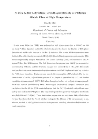
5. FIG. 1: Incident x-rays being scattered from atomic planes. Intensity of scattered x-rays
is maximum when the extra path-length traveled by adjacent scattered x-rays is equal to
2dsin(θ)
X - ray diffraction is a powerful and non - destructive technique that allows for the precise
structural characterization of crystalline materials. When an x-ray beam is incident on a
crystal plane of an atomic lattice, a portion of the beam will be scattered by the atoms and
a portion will be scattered by an adjacent, parallel crystalline plane(Fig. 1). The scattered
wave fronts created by the adjacent crystalline planes will have a phase lag because the
scattered x - rays must travel an additional path length 2dsin(θ), where d is the atomic
spacing. If this difference in path length is an integer number of wavelengths of the incident
light, then constructive interference occurs and the intensity of the scattered x - rays is
maximum. This analysis results in the well-known Bragg’s law (1) for diffraction from an
atomic lattice. X - ray diffraction has many useful application. Within the realm of thin
films x - ray diffraction can be used for phase identification, stress and strain analysis, film
quality and dislocation density, measuring roughness and thickness, as well as determining
film quality and grain orientation.
λ = 2dhklsin(θ) (1)
B. Methods
Characterization of thin film crystalline structures during annealing in air and vacuum
up to 1000°C was performed in situ using an Anton Paar 1100 Domed Hot Stage (DHS)
mounted to a PANalytical X’Pert Pro XRD system. A schematic diagram of the geometry
5
6. used for XRD scans is shown in Fig 2. Incident optics included a Cu - Kα radiation source,
1/2° divergent slit and parabolic x - ray mirror. Receiving optics included a 0.18 parallel
plate collimator, 0.02 soller slit and a proportional Xe detector. These optics were chosen
to make the incident and receiving x - rays beams as parallel as possible; this eliminates
variances in XRD spectra due to changes in sample thickness and changes in the XRD
alignment at high temperatures caused by thermal expansion. The application of these
optics inside the PANalytical X’Pert Pro XRD is shown in Fig. 3.
FIG. 2: Parallel beam geometry of the x-ray diffraction experiment showing the x-ray source,
incident beam optics, sample, diffracted beam optics, and detector.
FIG. 3: Image showing the inside of the PANalytical X’Pert Pro XRD system. Incident
optics are to the far right, sample stage and goniometer are center-most, and the diffracted,
or receiving optics are to the far left.
6
7. Samples were mounted on the DHS (Fig. 4a) which was attached to a PANalytical X’Pert
Pro XRD system (Fig. 4b). This novel sample heating stage includes an AlN heater that can
reach 1100°C, inconel sample clips to hold the thin film sample, and a carbon dome which
acts to contain the heat to a small volume while remaining x - ray transparent (although x -
rays enter and exit through the dome, there is only a slight attenuation of the x - ray beam).
The dome also allows for the sample to be subjected to pressures ranging from atmosphere
to 10−4
Torr.
(a) 1100 Anton Paar Domed Hot Stage: (1)
Carbon, x-ray transparent dome (2) AlN
heater stage (3) Inconel sample clips (4) con-
nection for ingas/vacuum and temperature
control
(b) PANalytical X’Pert Pro XRD system lo-
cated in the Laboratory for Surface Science and
Technology at the University of Maine
FIG. 4:
Annealing of the Pt/Si(100) film samples was carried out in either atmospheric pressuer
(760 Torr) or 10−4
Torr. XRD spectra were continuously recorded using Bragg - Brentano
7
8. geometry(Fig. 5). For experiments conducted in this study, samples underwent two types
of heat treatment: increasing temperature steps and isothermal holds. After an initial
room temperature (25°C) scan, the sample temperature was increased to 130°C and then
increased in 10°C steps thereafter. During each step, the temperature was held constant
while an XRD spectrum was recorded. Isothermal treatments were conducted at 1000°C
with XRD spectra being acquired approximately every 10 minutes. Due to time constraints,
only the air annealed sample was allowed to dwell at 1000°C.
FIG. 5: Angle of incidence(ω) is between the x-ray source and the sample. The diffracted
beam angle(2θ) is between the incident beam and the detector. Using this geometry the
source remains fixed while the sample rotates by the angle θ and the detector rotates by the
angle 2θ
C. Film Preparation
A 100 nm thick Platinum thin film was grown on an n-type Si(100) wafer using DC
sputtering in the LASST clean room by graduate student Robert Fryer. Si(100) wafer was
treated by buffered-oxide-etch in order to obtain a clean, oxide free Si surface prior to Pt
deposition. Sputter deposition of the Pt film was conducted using 300 W power, 3 mTorr of
Ar gas and a 99.999% pure platinum target. Following deposition, the Pt/Si sample was cut
into a size of approximately 5mmx20mm; these sample dimensions eliminated interference
by the sample stage during XRD characterization.
8
9. III. RESULTS AND DISCUSSION
A. Thermal Expansion of Pt Film
In situ XRD is an ideal tool for measuring thermal expansion of materials because 2θ
peak position can be directly correlated to crystal lattice spacing, which allows for the
examination of the response of materials to an increase in temperature. When a material
is heated, the energy of the crystal lattice increases which results in increased vibrational
motion of the atoms and a larger than average bond distance due to anharmonic motion.
For isotropic materials, 1-D or linear expansion can be assumed. The average displace-
ment of the atoms in a crystal lattice can be examined using the Boltzmann distribution(2).
x =
+∞
−∞
xe−(U(x)/kT)
+∞
−∞
e−(U(x)/kT)
dx (2)
For temperatures below the melting point of a material, thermal expansion can be
considered to be linear with temperature. The potential energy of the of atoms displaced
from equilibrium can be expressed as:
U(x) = cx2
− gx3
− fx4
(3)
Using this potential energy, equation 2 becomes:
x ∼=
3g
4c2
kT (4)
Therefore, the average displacement of atoms in a crystal lattice increases with temperature.
This linear expansion can be expressed as the fractional change in length:
9
10. ∆L
L0
= α∆T (5)
where the fractional change in length is determined by the 2θ peak position in Bragg’s law
for constructive interference.
The experiments to determine the thermal expansion of a Pt thin film were used as a
learning tool. These experiments were conducted in order to gain experience operating the
XRD system, properly aligning a sample, using the data collection software, and using the
DHS.
Figure 6 shows the results of in situ XRD experiments examining the response of a Pt
(111) peak to annealing. The peak shows a shift in position to a lower angle as temperature
is increased. This shift to a smaller angle correlates to an increasing atomic spacing within
the crystal lattice due to inverse nature of peak position (2θ) and atomic spacing predicted
by Bragg’s law.
FIG. 6: In situ thermal expansion of a Pt thin film deposited on a sapphire substrate.
Shown is a planar view of intensity as a function of both temperature and 2θ degrees.
Relative intensity is indicated by color
Figure 7 displays the fractional change in length determined from the results shown in
10
11. Figure 6 as a function of temperature. From the linear fit of the data, a coefficient of linear
expansion for the Pt film is determined to be 1.01 × 10⁻⁵
C−1
. The accepted bulk value
for the coefficient of linear expansion of Pt is 9 × 10⁻⁶
C−1
. The cause for the discrepancy
between the calculated value and the accepted value for the coefficient of linear expansion
is most likely due to differences in bond distances near the surface of the Pt film and within
the thin film as compared to the bond distance in bulk, 3-dimensional materials.
FIG. 7: Fractional change in length of a Pt thin film as a function of temperature. The
linear coefficient of thermal expansion, as determined by the slope of the fit, is 1.01 × 10⁻⁵
B. In Situ Measurements of Platinum Silicide Formation During Annealing from
25°C to 1000°C in Vacuum
In order to observe the formation of a PtSi phase due to solid - solid reaction of the
Pt/Si(100) sample, in situ XRD measurements were taken during heat treatment in vac-
uum (10−4
Torr). Figure 8 displays three XRD spectra at different times during the heat
treatment by steps: room temperature before annealing, at 1000°C, and room temperature
after annealing. At 1000°C it is observed that Pt, present before annealing, has been con-
sumed and two silicide grain orientations, PtSi(101) and PtSi(002), have formed. There are
several diffraction peaks (identified by *) present in the 1000°C and after annealing spectra,
that are not present in the as - deposited spectrum. These extra peaks are artifacts due to
the sample shifting during measurement resulting in additional diffraction peaks from the
11
12. sample stage. The sample shift on the stage occurred at approximately 870°C. Irregard-
less, the PtSi peaks are well defined and Figure 8 shows the Pt phase being almost entirely
consumed from the solid - solid reaction.
FIG. 8: XRD spectra from the Pt/Si(100) sample at (a) room temperature, (b) at 1000°C,
and (c) at room temperature after annealing. Peaks that are starred are due to diffraction
from the AlN sample heater. The AlN heater peaks are only present in (b) and (c) since, in
these cases, the sample shifted on the heater stage at about 870°C
Fig. 9 shows a detailed, 3-D, in situ map of the Pt - Si film during heat treatment
in vacuum(10−4
Torr). This color scale represents the natural log of the peak intensity
as a function of 2θ and temperature using a Matlab script (see Appendix: A). Figure 10
shows a planar view of the same data with the intensity plotted as contour lines, and labels
are displayed for various points of interest in the data: the black lines represent PtxSiy
compounds while the dotted and solid red lines represent artifacts due to the AlN sample
stage and Cu - Kβ peaks. At approximately 240°C, a polycrystalline PtSi phase is observed
to form resulting in the consumption of Pt. Comparing these peak positions to those in
the powder diffraction database [13, 14] gives evidence to the poly-crystalline layer being
composed of PtSi(101), PtSi(200), PtSi(220), Pt(200), PtSi(002), PtSi(112), and PtSi(022)
grain orientations. Higher temperatures result in the disappearance of all PtSi peaks except
12
13. PtSi(101) and PtSi(002) indicating that these grain continued to grow at the expense of the
other grain orientations. PtSi(002), as well as Pt (111) and PtSi(101) above 750°C, shows
a steady increase in peak intensity. This is most likely an indication of recrystallization
or grain growth. PtSi(002) shows a decrease in intensity between about 350°C and 700°C
with a steady increase in intensity thereafter. The initial decrease may be a result of the
attenuation of the scattered x -rays due to increased thermal motion of the atomic lattice
which is then compensated by subsequent recrystallization or grain growth.
FIG. 9: In situ XRD map of Pt thin film on Si(100) during annealing in vacuum. Shown is
the intensity of diffraction peaks as a function of temperature and 2θ degrees
.
13
14. FIG. 10: Planar view of in situ XRD map for Pt thin film on Si(100) from 25°C to 1000°C.
Peak intensities are represented by a color scale.
Fig. 11 displays the peak areas of the PtSi(101), PtSi(002), and Pt(111) peaks normalized
to the maximum value of the Pt(111) peak. The left y-axis represents a scale for the
PtSi(101) and PtSi(002) peaks while the right y-axis represents a scale for the Pt(111) peak.
Figure 12 shows the same results as Figure 11 but with a magnified y-axis scale in order
to show more detail in the Pt(111) and PtSi(101) area data at higher temperatures. An
interesting result shown from Figure 12 is that the Pt is not completely consumed. A very
small diffraction peak for Pt(111) persists throughout the treatment after the solid - solid
reaction and silicide formation as observed in Fig. 11. This could be explained by the
presence of a large Pt droplet on the surface. This droplet would have formed during the
DC sputtering film deposition process, which could not be completely react to form a PtSi
phase.
14
15. FIG. 11: Normalized area of the PtSi(101), Pt(111), and PtSi(002) peaks during annealing
in vacuum. Peak area was normalized to the Pt(111) peak.
From Figure 11, the initial silicide formation is observed at approximately 240°C while
the consumption of Pt begins at approximately 125°C. A cause for the discrepancy in the
temperatures of PtSi formation and Pt consumption is likely due to the initial PtSi grain size
being too small to be distinguishable from the background noise. At 850°C, the normalized
area of PtSi(101) is observed to increase and the normalized area of PtSi(002) is observed
to decrease. This may be an indication of grain growth of PtSi(101). However, this may
also be the result of the sample shifting on the sample stage. Thus, no conclusion should be
drawn from the observed data above 850°C.
15
16. FIG. 12: Normalized area of of Pt(111) and PtSi(101) peaks. This is the same data presented
in Fig. 10 but with a magnified scale in order to show more detail.
C. In Situ Measurements of Platinum Silicide Formation During Annealing from
25°C to 1000°C in air
The Pt/Si(100) solid state reaction was repeated in air. Figure 13 shows three XRD
spectra: an initial room temperature measurement, a 1000°C measurement, and a room
temperature measurement after annealing. Observed is a strong Pt(111) peak present before
annealing. The in situ measurement at 1000°C shows a Pt(111) peak that has increased
in intensity and that coexists with PtSi(101) and PtSi(002) peaks. These results indicate
some Pt - silicide formation. The persistent Pt(111) peak was unexpected, however. It was
expected that the Pt(111) peak would be fully consumed during the Pt - Si reaction, as it
was during vacuum treatments.
16
17. FIG. 13: XRD spectra of Pt thin film on Si(100) substrate during three steps of heat
treatment in air. Shown are XRD spectra at (a) room temperature before annealing, (b) at
1000°C, and (c) at room temperature after annealing.
Figure 14 shows the more detailed, 3-D in situ XRD map during annealing by steps. The
natural log of the intensity obtained via XRD is plotted as a function of both 2θ position
and temperature. Figure 15 shows a planar view of the same data with intensity plotted as
contour lines (a) as well as data obtained during isothermal treatment at 1000°C (b) and
displays labels for various points of interests in the data: the black lines represent PtxSiy
compounds while the dotted and solid red lines represent artifacts due to the AlN sample
stage and Cu - Kβ peaks.
From Figures 14 and 15, the decrease in peak intensity is evidence for the consumption
of Pt, and silicide formation is observed at approximately 330°C. At this temperature, the
results indicate formation of a poly-crystalline layer as was the case for heat treatment in
vacuum. At higher temperatures, it is observed that PtSi(101) and PtSi(002) experience
grain growth as indicated by the increase in their respective peak intensities and decrease in
the intensities of all other peaks besides that of Pt(111). From Fig. 15 it is observed that the
PtSi(101), Pt(111), and PtSi(002) peaks endure through both increasing temperature steps
and isothermal heat treatments. During temperature ramping, the PtSi(002) peak shows a
17
18. steady increase in intensity and the PtSi(101) peak shows a decrease in intensity between
550°C and 750°C with a steady increase thereafter. No major structural or morphological
changes were observed during the isothermal treatment.
FIG. 14: In situ XRD map of Pt thin film on Si(100) during annealing in air. Shown is the
intensity of diffraction peaks as a function of temperature and 2θ degrees
A key feature of both Figures 14 and 15 is that the Pt(111) peak at 39.76° 2θ endures
both the heat treatments. It has been shown that during annealing, Pt will be completely
consumed when treated in this way in vacuum or nitrogen environments. However, only
slight consumption of Pt is observed at approximately 330°C, as indicated by the silicide
formation and decrease in the Pt(111) peak intensity. Because the silicide formation is
facilitated via the simultaneous diffusion of Pt into the Si substrate and vice versa, a likely
18
19. cause of a sustained Pt phase is the presence of a diffusion barrier. It has been reported
[15] that SiO2 forms when Pt - Si films are annealed in air and the amorphous SiO2 phase
is believed to act as a diffusion barrier. The amorphous Si02 layer does not give an XRD
signal but may be a likely cause of the persistent Pt(111) peak.
FIG. 15: (a) In situ XRD maps in air of a Pt thin film on Si(100) after the heat treatment by
steps from 25°C to 1000°C in air, and (b) during the isothermal heat treatment at 1000°C.
Peak intensity is represented by the color scale.
Fig. 16 displays the peak areas of the PtSi(101), PtSi(002), and Pt(111) normalized to the
maximum value of the Pt(111) peak. The left y-axis represents a scale for the PtSi(101) and
PtSi(002) peaks, while the right y-axis represents a scale for the Pt(111) peak. Initial silicide
formation and Pt consumption is observed at approximately 320°C. Silicide formation and
consumption of Pt is observed to halt at approximately 330°C. Unlike annealing in vacuum,
there is no apparent lag between the temperature of initial Pt consumption and that of
19
20. the initial PtSi phase formation. The normalized area of the PtSi(002) peak is shown to
increase throughout the treatment, suggesting recrystallization, while the normalized area
of the PtSi(101) peak is shown to remain relatively unchanged after the initial formation.
The Pt(111) peak is observed to increase in area between 650°C and 750°C and is observed
to decrease in area thereafter.
FIG. 16: Normalized areas of the PtSi(101), Pt(111), and PtSi(002) peaks during annealing
in air. Peak areas are normalized to the Pt(111) peak.
IV. CONCLUSIONS
Solid state reaction was successfully used to form a PtSi phase from an as-deposited 100
nm thick Pt film on a clean Si(100) substrate in vacuum and atmospheric conditions. In situ
XRD at high temperatures reveals that vacuum annealing results in the complete consump-
tion of platinum to form a poly-crystalline PtSi layer composed of PtSi(101), PtSi(002),
PtSi(200), PtSi(220), PtSi(112), and PtSi(022) grains at approximately 240°C; PtSi(101)
and PtSi(002) are the preferred orientation that remain after final heat treatments. An-
nealing in air resulted in the solid state reaction of Pt/Si(100) to the PtSi phase being
interrupted by the formation of an amorphous SiO2 layer that acts as a diffusion barrier.
The same PtSi poly-crystalline layer forms as in vacuum, but the reaction goes to comple-
tion at approximately 330°C with PtSi(101) and PtSi(002) being the preferred orientations.
Extended annealing at 1000°C for 10 hours resulted in no morphological change in the PtSi
film.
A large portion of this work was dedicated to developing a technique to acquire in situ
XRD spectra at high temperatures using an Anton Paar 1100 DHS and PANalytical X’Pert
Pro XRD system. This was accomplished by developing a procedure to properly operate
the DHS, select x-ray optics to acquire meaningful and accurate data, as well as developing
Matlab tools for data analysis and visualization, and formatting the report in Latex; this
work was my first introduction to Matlab and Latex.
The major conclusion can be summarized as follows:
• Successfully developed and implemented technique to acquire in situ XRD spectra up
20
21. to 1000°C using a 1100 Anton Paar Domed Hot Stage and PANalytical X’Pert Pro
XRD system
1. Procedure for operation of DHS
2. Optics to acquire accurate date
3. Matlab tools for data analysis and visualization
• Under vacuum conditions Pt/Si(100) undergoes solid state reaction to form a PtSi
phase
1. PtSi(101), PtSi(200), PtSi(020), PtSi(220), PtSi(002), PtSi(112), and PtSi(022)
initially form a polycrystalline layer at approximately 240°C.
2. PtSi(101) and PtSi(002) are the preferred orientations that develop during heat
treatment.
3. Trace amounts of Pt(111) persist throughout the heat treatment in vacuum.
• In air, the solid state reaction of Pt/Si(100) to the PtSi phase is hindered by an
amorphous SiO2 layer forming and acting as a diffusion barrier
1. The same polycrystalline layer forms as did in vacuum but at at a higher tem-
perature of approximately 330°C.
2. PtSi(101) and PtSi(002) are the preferred orientation observed during the heat
treatment in air.
3. Extended annealing at 1000°C for approximately 10 hours results in no morpho-
logical change in the PtSi film or additional consumption of Pt.
V. SUGGESTIONS FOR FURTHER RESEARCH
1. Perform in situ experiments using different substrates (i.e. Si(100) vs. Si(111)).
2. Perform in situ experiments using different thicknesses of as - deposited Pt films.
3. Purposely grow an SiO2 layer to hinder the diffusion in vacuum and compare results
of the air anneal.
21
22. 4. Perform in situ experiments in different atmospheres using the gas delivery system
being developed by Matthew Curti for his senior project at LASST.
Acknowledgments
This work was performed as a capstone research project for a Bachelors of Science in
Physics at the University of Maine. I would like to thank my research adviser Dr. Robert
Lad, my capstone adviser Dr. James McClymer, LASST research scientist Dr. George
Bernhardt, graduate students Robert Fryer and David Stewart, as well as my undergraduate
colleague, Matthew Curti, for their valuable insights and support. This work was funded
by the National Science Foundation (NSF) under Sustainable Chemistry, Engineering &
Materials (SusChEM) grant #1309983.
22
23. References
[1] C. Fitz, M. Goldbach, A. Dupont, and S. Schmidbauer. Silicides as contact material for
DRAM applications. Microelectronic Engineering, 82(3-4):460–466, DEC 2005. PT: J; CT:
European Workshop on Materials for Advanced Metallization; CY: MAR 06-09, 2005; CL:
Dresden, GERMANY; SI: SI; UT: WOS:000234236100041.
[2] N. S. Stoloff, C. T. Liu, and S. C. Deevi. Emerging applications of intermetallics. Inter-
metallics, 8(9-11):1313–1320, SEP-NOV 2000 2000. PT: J; SI: SI; CT: International Sym-
posium on Intermetallics for the 3rd Millennium - A Symposium Dedicated to RW Cahn;
CY: NOV 01-04, 1999; CL: CINCINNATI, OHIO; SP: ASM Int, Intermetall Mat Comm Crit
Technol Sector; US DOE; TC: 286; UT: WOS:000165753700039.
[3] Omar Abbes, Khalid Hoummada, Dominique Mangelinck, and Veronique Carron. Formation
of Pt silicide on doped Si: Kinetics and stress. Thin Solid Films, 542:174–179, SEP 2 2013
2013. PT: J; TC: 2; UT: WOS:000323859400029.
[4] P. W. Pellegrini, C. E. Ludington, and M. M. Weeks. The dependence of schottky-barrier po-
tential on substrate orientation in PtSi infrared diodes. Journal of Applied Physics, 67(3):1417–
1420, FEB 1 1990 1990. PT: J; TC: 28; UT: WOS:A1990CL92000044.
[5] Manish K. Niranjan, Stefan Zollner, Leonard Kleinman, and Alexander A. Demkov. Theoreti-
cal investigation of PtSi surface energies and work functions. Physical Review B, 73(19):195332,
MAY 2006 2006. PT: J; TC: 23; UT: WOS:000237950400100.
[6] V. W. L. Chin, M. A. Green, and J. W. V. Storey. Current transport mechanisms studied
by i-v-t and ir photoemission measurements on a p-doped PtSi schottky diode. Solid-State
Electronics, 36(8):1107–1116, AUG 1993 1993. PT: J; TC: 26; UT: WOS:A1993LK58000005.
[7] V. Carron, F. Nemouchi, Y. Morand, T. Poiroux, M. Vinet, S. Bernasconi, O. Louveau,
D. Lafond, V. Delaye, F. Allain, S. Minoret, L. Vandroux, and T. Billon. Platinum Silicide
Metallic Source & Drain Process Optimization for FDSOI pMOSFETs. 2009 2009. PT: B;
CT: IEEE International SOI Conference 2009; CY: OCT 05-08, 2009; CL: Foster City, CA;
SP: IEEE; TC: 0; UT: WOS:000276151400045.
[8] R.T. Fryer, R.J. Lad. Electrical conductivity and thermal stability of Pt3Si, Pt2Si, and PtSi
films grown by e-beam co-evaporation. Journal of Alloys and Compounds, (2016, in press).
23
24. [9] R.T. Fryer, R.J. Lad. Comparison of PtSi films grown by solid-state reaction and by e-beam
co-evaporation: Thermal stability in air at 1000 C. MRS Advances, (2016, in press).
[10] R.J. Lad, D.M. Stewart, R.T. Fryer, J.C. Sell, D.J. Frankel, G.P. Bernhardt, R.W. Meulenberg.
Electrical conductivity of Pt-Zr-B and Pt-Si thin films for use in high temperature harsh
environments. MRS Advances, (2016, in press).
[11] L. E. Calvet, H. Luebben, M. A. Reed, C. Wang, J. P. Snyder, and J. R. Tucker. Subthreshold
and scaling of PtSi schottky barrier mosfets. Superlattices and Microstructures, 28(5-6):501–
506, NOV-DEC 2000 2000. PT: J; CT: 5th Silicon Nanoelectronics Workshop; CY: JUN
11-12, 2000; CL: HONOLULU, HAWAII; SP: Inst Elect & Electr Engineers; TC: 21; UT:
WOS:000165917400026.
[12] Miroslav Sumega and Vladimir Ac. Study of PtSi/TiW vs PtSi/Ti-TiN contact structures.
Journal of Electrical Engineering-Elektrotechnicky Casopis, 60(5):287–290, SEP-OCT 2009
2009. PT: J; CT: 15th International Conference on Applied Physics of Condesned Matter;
CY: JUN 24-26, 2009; CL: Bystra, SLOVAKIA; TC: 1; UT: WOS:000271846100010.
[13] International Centre for Diffraction Data, Powder Diffraction File, Card No. 04-003-0990.
[14] International Centre for Diffraction Data, Powder Diffraction File, Card No. 00-004-0802.
[15] R. J. Blattner, C. A. Evans, S. S. Lau, J. W. Mayer, and B. M. Ullrich. Effect of oxidiz-
ing ambients on platinum silicide formation .2. Auger and backscattering analyses. Jour-
nal of the Electrochemical Society, 122(12):1732–1736, 1975 1975. PT: J; TC: 47; UT:
WOS:A1975AX54300040.
24
25. VI. APPENDIX
A: Matlab code to generate surface plots
% Import excel data. Data sets must be converted to .xls using powDLL
x = xlsread('xls file'); % Data
angle = x(:, 1); % Extract angle from spreadsheet
temp = [25, 130:10:1000]; % Define temp range
% Configure data set
% Removes duplicate data and deletes empty columns
r = size(x, 1); % total rows
c = size(x, 2); % total columns
d = 2; % rows in each data set
n = 1; % remove first n columns in each data set
x(:, mod(1:c, d) <= n & mod(1:c, d) > 0) = [];
data = x;
figure(1)
surf(temp, angle, log(data), ...
'FaceColor', 'interp', ...
'EdgeColor', 'none', ...
'FaceLighting', 'gouraud');
% Add axis label
xlabel('Temperature (C)');
ylabel('2theta (deg)');
zlabel('ln(Intensity) (arb)');
% Set axis limits
25
29. B: Considerations
Economic/Sustainability
Significant cost savings can be made by utilizing stable thin film electrodes and sensor
devices to optimize the servicing of equipment used in high temperature environments. Many
high temperature industrial environments (e.g. turbine engines, power plate boilers, oil
drilling) require regular monitoring in order to determine maintenance needs. By employing
sensors that are stable at high temperatures, industry participants can increase the lifetime
of expensive equipment and increase overall sustainability.
Environmental
By optimizing the maintenance of industrial machinery with wireless sensors, process effi-
ciency and overall energy consumption may be reduced. This could alter the environmental
impact of many industrial processes.
Manufacturability
The films used in this study were produced in The LASST, UHV, thin film deposition
chamber by graduate student Robert Fryer.
Ethical
Standard ethical practices were followed during research to ensure general safety and in
the reporting of the research findings.
Health and Safety
This project required certification in x-ray safety and general lab safety in order to operate
the laboratory equipment needed. Both certification required attending a safety training
course. A seminar in research ethics was also a required in order to receive NSF funding for
this project.
29