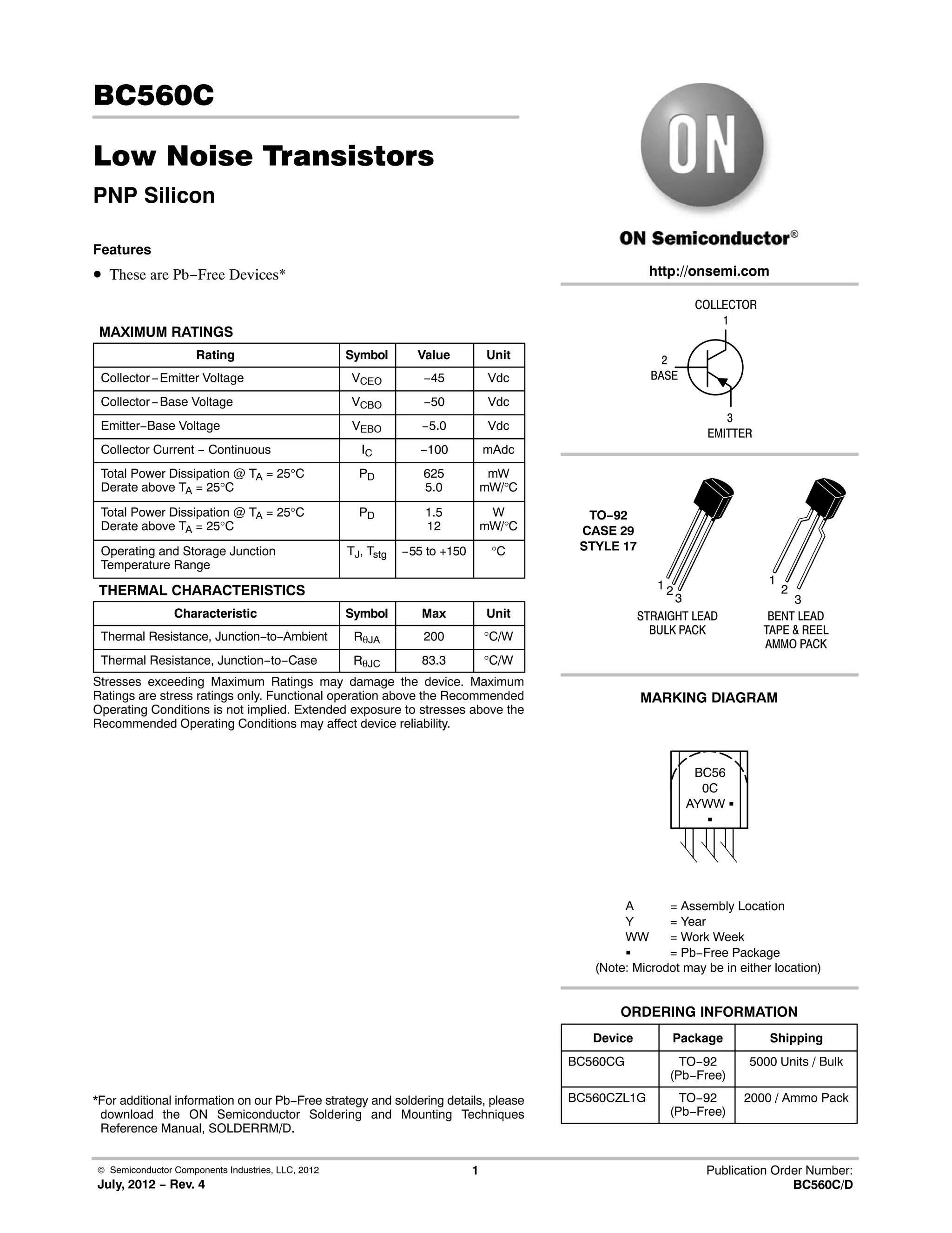
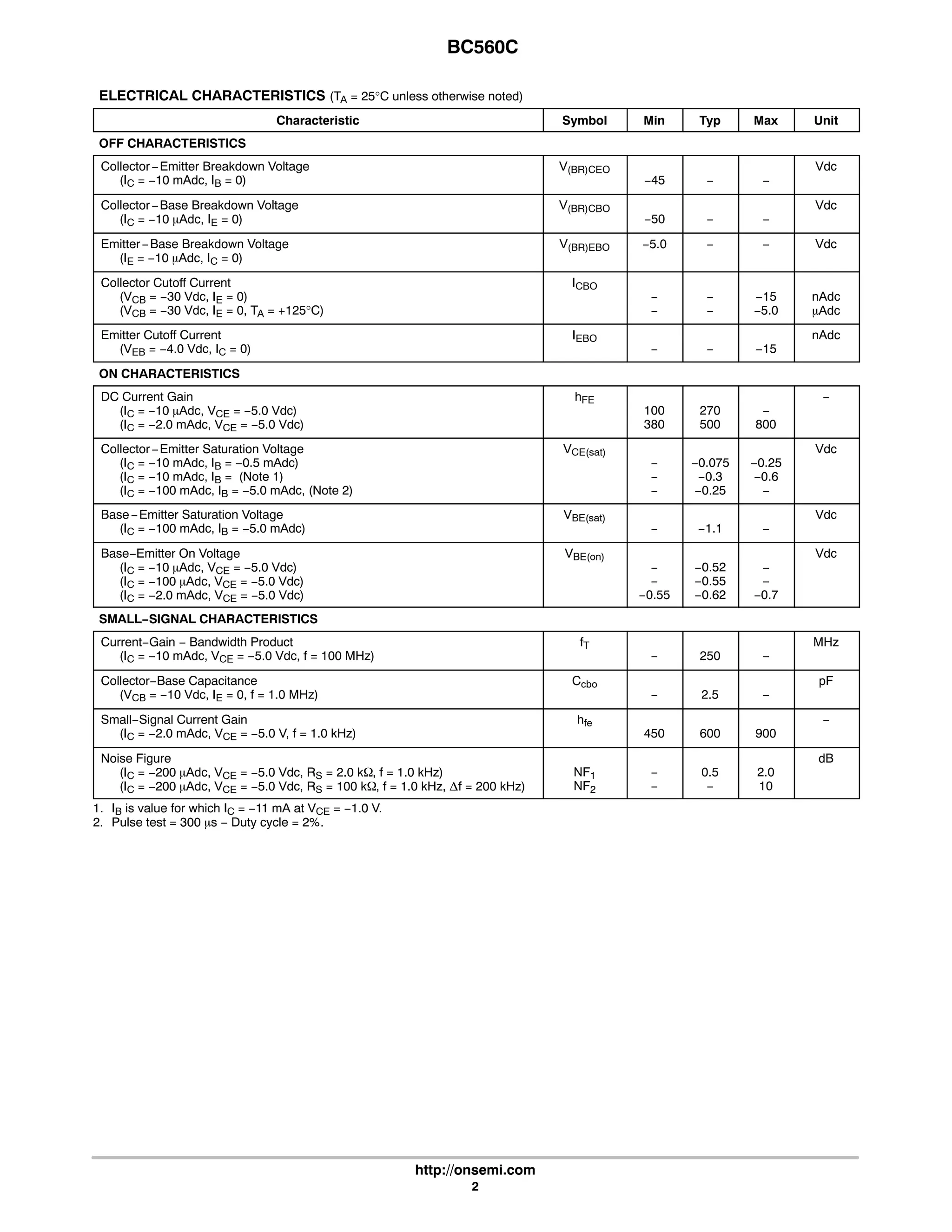
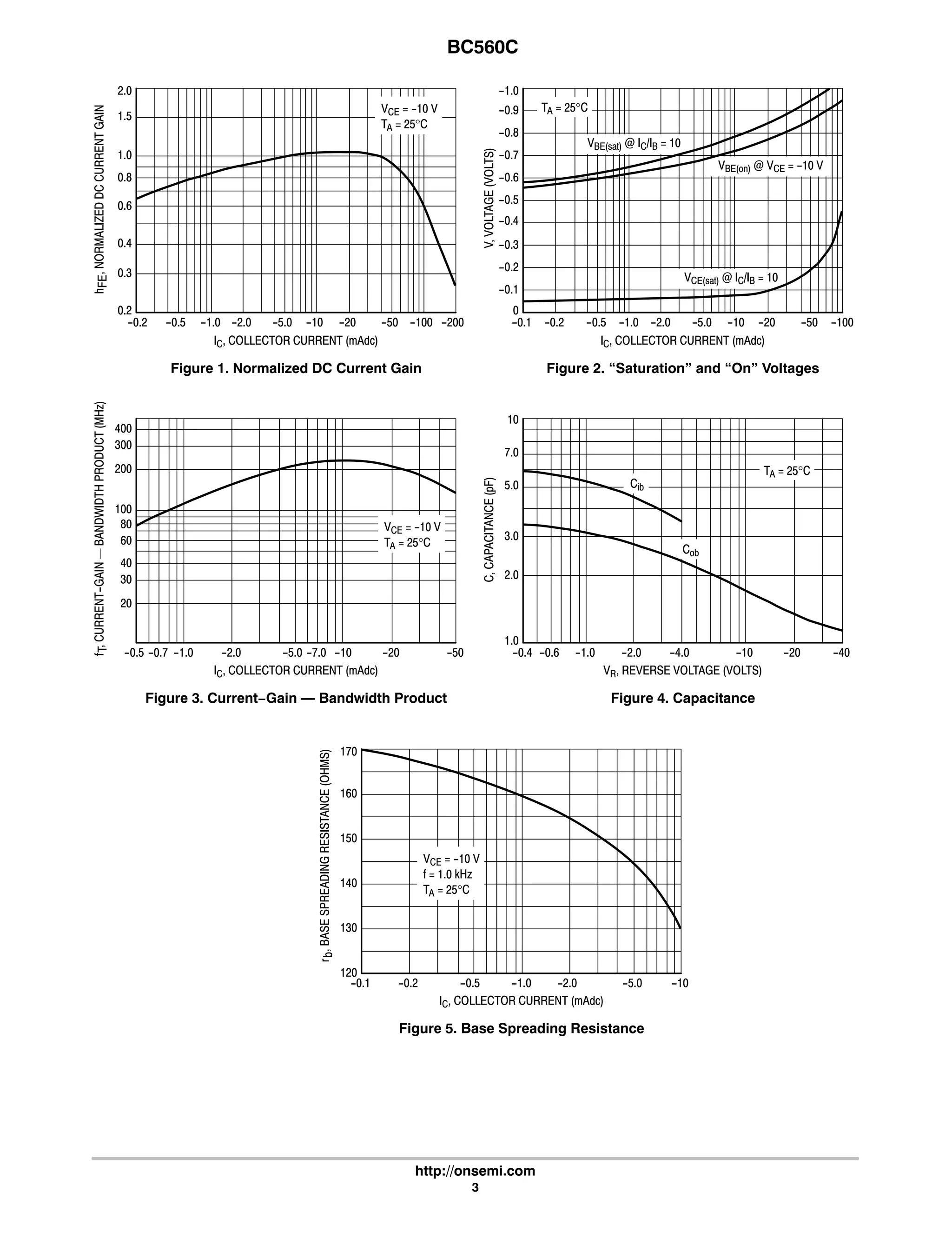
© Semiconductor Components Industries, LLC, 2012
July, 2012 − Rev. 4
1 Publication Order Number:
BC560C/D
BC560C
Low Noise Transistors
PNP Silicon
Features
• These are Pb−Free Devices*
MAXIMUM RATINGS
Rating Symbol Value Unit
Collector−Emitter Voltage VCEO −45 Vdc
Collector−Base Voltage VCBO −50 Vdc
Emitter−Base Voltage VEBO −5.0 Vdc
Collector Current − Continuous IC −100 mAdc
Total Power Dissipation @ TA = 25°C
Derate above TA = 25°C
PD 625
5.0
mW
mW/°C
Total Power Dissipation @ TA = 25°C
Derate above TA = 25°C
PD 1.5
12
W
mW/°C
Operating and Storage Junction
Temperature Range
TJ, Tstg −55 to +150 °C
THERMAL CHARACTERISTICS
Characteristic Symbol Max Unit
Thermal Resistance, Junction−to−Ambient RqJA 200 °C/W
Thermal Resistance, Junction−to−Case RqJC 83.3 °C/W
Stresses exceeding Maximum Ratings may damage the device. Maximum
Ratings are stress ratings only. Functional operation above the Recommended
Operating Conditions is not implied. Extended exposure to stresses above the
Recommended Operating Conditions may affect device reliability.
*For additional information on our Pb−Free strategy and soldering details, please
download the ON Semiconductor Soldering and Mounting Techniques
Reference Manual, SOLDERRM/D.
http://onsemi.com
COLLECTOR
1
2
BASE
3
EMITTER
Device Package Shipping
ORDERING INFORMATION
BC560CG TO−92
(Pb−Free)
5000 Units / Bulk
BC560CZL1G TO−92
(Pb−Free)
2000 / Ammo Pack
1 2
3
1
2
BENT LEAD
TAPE & REEL
AMMO PACK
STRAIGHT LEAD
BULK PACK
3
TO−92
CASE 29
STYLE 17
MARKING DIAGRAM
BC56
0C
AYWW G
G
A = Assembly Location
Y = Year
WW = Work Week
G = Pb−Free Package
(Note: Microdot may be in either location)
BC560C
http://onsemi.com
2
ELECTRICAL CHARACTERISTICS (TA = 25°C unless otherwise noted)
Characteristic Symbol Min Typ Max Unit
OFF CHARACTERISTICS
Collector−Emitter Breakdown Voltage
(IC = −10 mAdc, IB = 0)
V(BR)CEO
−45 − −
Vdc
Collector−Base Breakdown Voltage
(IC = −10 mAdc, IE = 0)
V(BR)CBO
−50 − −
Vdc
Emitter−Base Breakdown Voltage
(IE = −10 mAdc, IC = 0)
V(BR)EBO −5.0 − − Vdc
Collector Cutoff Current
(VCB = −30 Vdc, IE = 0)
(VCB = −30 Vdc, IE = 0, TA = +125°C)
ICBO
−
−
−
−
−15
−5.0
nAdc
mAdc
Emitter Cutoff Current
(VEB = −4.0 Vdc, IC = 0)
IEBO
− − −15
nAdc
ON CHARACTERISTICS
DC Current Gain
(IC = −10 mAdc, VCE = −5.0 Vdc)
(IC = −2.0 mAdc, VCE = −5.0 Vdc)
hFE
100
380
270
500
−
800
−
Collector−Emitter Saturation Voltage
(IC = −10 mAdc, IB = −0.5 mAdc)
(IC = −10 mAdc, IB = (Note 1)
(IC = −100 mAdc, IB = −5.0 mAdc, (Note 2)
VCE(sat)
−
−
−
−0.075
−0.3
−0.25
−0.25
−0.6
−
Vdc
Base−Emitter Saturation Voltage
(IC = −100 mAdc, IB = −5.0 mAdc)
VBE(sat)
− −1.1 −
Vdc
Base−Emitter On Voltage
(IC = −10 mAdc, VCE = −5.0 Vdc)
(IC = −100 mAdc, VCE = −5.0 Vdc)
(IC = −2.0 mAdc, VCE = −5.0 Vdc)
VBE(on)
−
−
−0.55
−0.52
−0.55
−0.62
−
−
−0.7
Vdc
SMALL−SIGNAL CHARACTERISTICS
Current−Gain − Bandwidth Product
(IC = −10 mAdc, VCE = −5.0 Vdc, f = 100 MHz)
fT
− 250 −
MHz
Collector−Base Capacitance
(VCB = −10 Vdc, IE = 0, f = 1.0 MHz)
Ccbo
− 2.5 −
pF
Small−Signal Current Gain
(IC = −2.0 mAdc, VCE = −5.0 V, f = 1.0 kHz)
hfe
450 600 900
−
Noise Figure
(IC = −200 mAdc, VCE = −5.0 Vdc, RS = 2.0 kW, f = 1.0 kHz)
(IC = −200 mAdc, VCE = −5.0 Vdc, RS = 100 kW, f = 1.0 kHz, Df = 200 kHz)
NF1
NF2
−
−
0.5
−
2.0
10
dB
1. IB is value for which IC = −11 mA at VCE = −1.0 V.
2. Pulse test = 300 ms − Duty cycle = 2%.
BC560C
http://onsemi.com
3
2.0
1.5
1.0
0.2
0.3
0.4
0.6
0.8
-0.2
IC, COLLECTOR CURRENT (mAdc)
Figure 1. Normalized DC Current Gain
hFE,NORMALIZEDDCCURRENTGAIN
VCE = -10 V
TA = 25°C
-1.0
-0.9
-0.8
-0.7
-0.6
-0.5
-0.4
-0.3
-0.2
-0.1
0
-0.2-0.1 -0.5 -1.0 -2.0 -5.0 -10 -20 -50 -100
IC, COLLECTOR CURRENT (mAdc)
Figure 2. “Saturation” and “On” Voltages
V,VOLTAGE(VOLTS)
TA = 25°C
VBE(sat) @ IC/IB = 10
VBE(on) @ VCE = -10 V
VCE(sat) @ IC/IB = 10
400
20
30
40
60
80
100
200
300
-0.5
IC, COLLECTOR CURRENT (mAdc)
Figure 3. Current−Gain — Bandwidth Product
fT,CURRENT-GAIN—BANDWIDTHPRODUCT(MHz)
C,CAPACITANCE(pF)
10
1.0
2.0
3.0
5.0
7.0
-0.4 -0.6 -1.0 -2.0 -4.0 -10 -20 -40
VR, REVERSE VOLTAGE (VOLTS)
Figure 4. Capacitance
TA = 25°C
Cib
Cob
rb,BASESPREADINGRESISTANCE(OHMS)
170
160
150
140
130
120
-10-0.1 -0.2 -0.5 -1.0 -2.0 -5.0
IC, COLLECTOR CURRENT (mAdc)
Figure 5. Base Spreading Resistance
VCE = -10 V
f = 1.0 kHz
TA = 25°C
-0.5 -1.0 -2.0 -5.0 -10 -20 -50 -100 -200
VCE = -10 V
TA = 25°C
-0.7 -1.0 -2.0 -5.0 -10-7.0 -20 -50
BC560C
http://onsemi.com
4
PACKAGE DIMENSIONS
TO−92 (TO−226)
CASE 29−11
ISSUE AM
NOTES:
1. DIMENSIONING AND TOLERANCING PER ANSI
Y14.5M, 1982.
2. CONTROLLING DIMENSION: INCH.
3. CONTOUR OF PACKAGE BEYOND DIMENSION R
IS UNCONTROLLED.
4. LEAD DIMENSION IS UNCONTROLLED IN P AND
BEYOND DIMENSION K MINIMUM.
R
A
P
J
L
B
K
G
H
SECTION X−X
CV
D
N
N
X X
SEATING
PLANE DIM MIN MAX MIN MAX
MILLIMETERSINCHES
A 0.175 0.205 4.45 5.20
B 0.170 0.210 4.32 5.33
C 0.125 0.165 3.18 4.19
D 0.016 0.021 0.407 0.533
G 0.045 0.055 1.15 1.39
H 0.095 0.105 2.42 2.66
J 0.015 0.020 0.39 0.50
K 0.500 --- 12.70 ---
L 0.250 --- 6.35 ---
N 0.080 0.105 2.04 2.66
P --- 0.100 --- 2.54
R 0.115 --- 2.93 ---
V 0.135 --- 3.43 ---
1
NOTES:
1. DIMENSIONING AND TOLERANCING PER
ASME Y14.5M, 1994.
2. CONTROLLING DIMENSION: MILLIMETERS.
3. CONTOUR OF PACKAGE BEYOND
DIMENSION R IS UNCONTROLLED.
4. LEAD DIMENSION IS UNCONTROLLED IN P
AND BEYOND DIMENSION K MINIMUM.
R
A
P
J
B
K
G
SECTION X−X
C
V
D
N
X X
SEATING
PLANE DIM MIN MAX
MILLIMETERS
A 4.45 5.20
B 4.32 5.33
C 3.18 4.19
D 0.40 0.54
G 2.40 2.80
J 0.39 0.50
K 12.70 ---
N 2.04 2.66
P 1.50 4.00
R 2.93 ---
V 3.43 ---
1
T
STRAIGHT LEAD
BULK PACK
BENT LEAD
TAPE & REEL
AMMO PACK
STYLE 17:
PIN 1. COLLECTOR
2. BASE
3. EMITTER
ON Semiconductor and are registered trademarks of Semiconductor Components Industries, LLC (SCILLC). SCILLC owns the rights to a number of patents, trademarks,
copyrights, trade secrets, and other intellectual property. A listing of SCILLC’s product/patent coverage may be accessed at www.onsemi.com/site/pdf/Patent−Marking.pdf. SCILLC
reserves the right to make changes without further notice to any products herein. SCILLC makes no warranty, representation or guarantee regarding the suitability of its products for any
particular purpose, nor does SCILLC assume any liability arising out of the application or use of any product or circuit, and specifically disclaims any and all liability, including without
limitation special, consequential or incidental damages. “Typical” parameters which may be provided in SCILLC data sheets and/or specifications can and do vary in different applications
and actual performance may vary over time. All operating parameters, including “Typicals” must be validated for each customer application by customer’s technical experts. SCILLC
does not convey any license under its patent rights nor the rights of others. SCILLC products are not designed, intended, or authorized for use as components in systems intended for
surgical implant into the body, or other applications intended to support or sustain life, or for any other application in which the failure of the SCILLC product could create a situation where
personal injury or death may occur. Should Buyer purchase or use SCILLC products for any such unintended or unauthorized application, Buyer shall indemnify and hold SCILLC and
its officers, employees, subsidiaries, affiliates, and distributors harmless against all claims, costs, damages, and expenses, and reasonable attorney fees arising out of, directly or indirectly,
any claim of personal injury or death associated with such unintended or unauthorized use, even if such claim alleges that SCILLC was negligent regarding the design or manufacture
of the part. SCILLC is an Equal Opportunity/Affirmative Action Employer. This literature is subject to all applicable copyright laws and is not for resale in any manner.
PUBLICATION ORDERING INFORMATION
N. American Technical Support: 800−282−9855 Toll Free
USA/Canada
Europe, Middle East and Africa Technical Support:
Phone: 421 33 790 2910
Japan Customer Focus Center
Phone: 81−3−5817−1050
BC560C/D
LITERATURE FULFILLMENT:
Literature Distribution Center for ON Semiconductor
P.O. Box 5163, Denver, Colorado 80217 USA
Phone: 303−675−2175 or 800−344−3860 Toll Free USA/Canada
Fax: 303−675−2176 or 800−344−3867 Toll Free USA/Canada
Email: orderlit@onsemi.com
ON Semiconductor Website: www.onsemi.com
Order Literature: http://www.onsemi.com/orderlit
For additional information, please contact your local
Sales Representative

Original PNP Transistor BC560C BC560 560 TO-92 New

  • 1.
    © Semiconductor ComponentsIndustries, LLC, 2012 July, 2012 − Rev. 4 1 Publication Order Number: BC560C/D BC560C Low Noise Transistors PNP Silicon Features • These are Pb−Free Devices* MAXIMUM RATINGS Rating Symbol Value Unit Collector−Emitter Voltage VCEO −45 Vdc Collector−Base Voltage VCBO −50 Vdc Emitter−Base Voltage VEBO −5.0 Vdc Collector Current − Continuous IC −100 mAdc Total Power Dissipation @ TA = 25°C Derate above TA = 25°C PD 625 5.0 mW mW/°C Total Power Dissipation @ TA = 25°C Derate above TA = 25°C PD 1.5 12 W mW/°C Operating and Storage Junction Temperature Range TJ, Tstg −55 to +150 °C THERMAL CHARACTERISTICS Characteristic Symbol Max Unit Thermal Resistance, Junction−to−Ambient RqJA 200 °C/W Thermal Resistance, Junction−to−Case RqJC 83.3 °C/W Stresses exceeding Maximum Ratings may damage the device. Maximum Ratings are stress ratings only. Functional operation above the Recommended Operating Conditions is not implied. Extended exposure to stresses above the Recommended Operating Conditions may affect device reliability. *For additional information on our Pb−Free strategy and soldering details, please download the ON Semiconductor Soldering and Mounting Techniques Reference Manual, SOLDERRM/D. http://onsemi.com COLLECTOR 1 2 BASE 3 EMITTER Device Package Shipping ORDERING INFORMATION BC560CG TO−92 (Pb−Free) 5000 Units / Bulk BC560CZL1G TO−92 (Pb−Free) 2000 / Ammo Pack 1 2 3 1 2 BENT LEAD TAPE & REEL AMMO PACK STRAIGHT LEAD BULK PACK 3 TO−92 CASE 29 STYLE 17 MARKING DIAGRAM BC56 0C AYWW G G A = Assembly Location Y = Year WW = Work Week G = Pb−Free Package (Note: Microdot may be in either location)
  • 2.
    BC560C http://onsemi.com 2 ELECTRICAL CHARACTERISTICS (TA= 25°C unless otherwise noted) Characteristic Symbol Min Typ Max Unit OFF CHARACTERISTICS Collector−Emitter Breakdown Voltage (IC = −10 mAdc, IB = 0) V(BR)CEO −45 − − Vdc Collector−Base Breakdown Voltage (IC = −10 mAdc, IE = 0) V(BR)CBO −50 − − Vdc Emitter−Base Breakdown Voltage (IE = −10 mAdc, IC = 0) V(BR)EBO −5.0 − − Vdc Collector Cutoff Current (VCB = −30 Vdc, IE = 0) (VCB = −30 Vdc, IE = 0, TA = +125°C) ICBO − − − − −15 −5.0 nAdc mAdc Emitter Cutoff Current (VEB = −4.0 Vdc, IC = 0) IEBO − − −15 nAdc ON CHARACTERISTICS DC Current Gain (IC = −10 mAdc, VCE = −5.0 Vdc) (IC = −2.0 mAdc, VCE = −5.0 Vdc) hFE 100 380 270 500 − 800 − Collector−Emitter Saturation Voltage (IC = −10 mAdc, IB = −0.5 mAdc) (IC = −10 mAdc, IB = (Note 1) (IC = −100 mAdc, IB = −5.0 mAdc, (Note 2) VCE(sat) − − − −0.075 −0.3 −0.25 −0.25 −0.6 − Vdc Base−Emitter Saturation Voltage (IC = −100 mAdc, IB = −5.0 mAdc) VBE(sat) − −1.1 − Vdc Base−Emitter On Voltage (IC = −10 mAdc, VCE = −5.0 Vdc) (IC = −100 mAdc, VCE = −5.0 Vdc) (IC = −2.0 mAdc, VCE = −5.0 Vdc) VBE(on) − − −0.55 −0.52 −0.55 −0.62 − − −0.7 Vdc SMALL−SIGNAL CHARACTERISTICS Current−Gain − Bandwidth Product (IC = −10 mAdc, VCE = −5.0 Vdc, f = 100 MHz) fT − 250 − MHz Collector−Base Capacitance (VCB = −10 Vdc, IE = 0, f = 1.0 MHz) Ccbo − 2.5 − pF Small−Signal Current Gain (IC = −2.0 mAdc, VCE = −5.0 V, f = 1.0 kHz) hfe 450 600 900 − Noise Figure (IC = −200 mAdc, VCE = −5.0 Vdc, RS = 2.0 kW, f = 1.0 kHz) (IC = −200 mAdc, VCE = −5.0 Vdc, RS = 100 kW, f = 1.0 kHz, Df = 200 kHz) NF1 NF2 − − 0.5 − 2.0 10 dB 1. IB is value for which IC = −11 mA at VCE = −1.0 V. 2. Pulse test = 300 ms − Duty cycle = 2%.
  • 3.
    BC560C http://onsemi.com 3 2.0 1.5 1.0 0.2 0.3 0.4 0.6 0.8 -0.2 IC, COLLECTOR CURRENT(mAdc) Figure 1. Normalized DC Current Gain hFE,NORMALIZEDDCCURRENTGAIN VCE = -10 V TA = 25°C -1.0 -0.9 -0.8 -0.7 -0.6 -0.5 -0.4 -0.3 -0.2 -0.1 0 -0.2-0.1 -0.5 -1.0 -2.0 -5.0 -10 -20 -50 -100 IC, COLLECTOR CURRENT (mAdc) Figure 2. “Saturation” and “On” Voltages V,VOLTAGE(VOLTS) TA = 25°C VBE(sat) @ IC/IB = 10 VBE(on) @ VCE = -10 V VCE(sat) @ IC/IB = 10 400 20 30 40 60 80 100 200 300 -0.5 IC, COLLECTOR CURRENT (mAdc) Figure 3. Current−Gain — Bandwidth Product fT,CURRENT-GAIN—BANDWIDTHPRODUCT(MHz) C,CAPACITANCE(pF) 10 1.0 2.0 3.0 5.0 7.0 -0.4 -0.6 -1.0 -2.0 -4.0 -10 -20 -40 VR, REVERSE VOLTAGE (VOLTS) Figure 4. Capacitance TA = 25°C Cib Cob rb,BASESPREADINGRESISTANCE(OHMS) 170 160 150 140 130 120 -10-0.1 -0.2 -0.5 -1.0 -2.0 -5.0 IC, COLLECTOR CURRENT (mAdc) Figure 5. Base Spreading Resistance VCE = -10 V f = 1.0 kHz TA = 25°C -0.5 -1.0 -2.0 -5.0 -10 -20 -50 -100 -200 VCE = -10 V TA = 25°C -0.7 -1.0 -2.0 -5.0 -10-7.0 -20 -50
  • 4.
    BC560C http://onsemi.com 4 PACKAGE DIMENSIONS TO−92 (TO−226) CASE29−11 ISSUE AM NOTES: 1. DIMENSIONING AND TOLERANCING PER ANSI Y14.5M, 1982. 2. CONTROLLING DIMENSION: INCH. 3. CONTOUR OF PACKAGE BEYOND DIMENSION R IS UNCONTROLLED. 4. LEAD DIMENSION IS UNCONTROLLED IN P AND BEYOND DIMENSION K MINIMUM. R A P J L B K G H SECTION X−X CV D N N X X SEATING PLANE DIM MIN MAX MIN MAX MILLIMETERSINCHES A 0.175 0.205 4.45 5.20 B 0.170 0.210 4.32 5.33 C 0.125 0.165 3.18 4.19 D 0.016 0.021 0.407 0.533 G 0.045 0.055 1.15 1.39 H 0.095 0.105 2.42 2.66 J 0.015 0.020 0.39 0.50 K 0.500 --- 12.70 --- L 0.250 --- 6.35 --- N 0.080 0.105 2.04 2.66 P --- 0.100 --- 2.54 R 0.115 --- 2.93 --- V 0.135 --- 3.43 --- 1 NOTES: 1. DIMENSIONING AND TOLERANCING PER ASME Y14.5M, 1994. 2. CONTROLLING DIMENSION: MILLIMETERS. 3. CONTOUR OF PACKAGE BEYOND DIMENSION R IS UNCONTROLLED. 4. LEAD DIMENSION IS UNCONTROLLED IN P AND BEYOND DIMENSION K MINIMUM. R A P J B K G SECTION X−X C V D N X X SEATING PLANE DIM MIN MAX MILLIMETERS A 4.45 5.20 B 4.32 5.33 C 3.18 4.19 D 0.40 0.54 G 2.40 2.80 J 0.39 0.50 K 12.70 --- N 2.04 2.66 P 1.50 4.00 R 2.93 --- V 3.43 --- 1 T STRAIGHT LEAD BULK PACK BENT LEAD TAPE & REEL AMMO PACK STYLE 17: PIN 1. COLLECTOR 2. BASE 3. EMITTER ON Semiconductor and are registered trademarks of Semiconductor Components Industries, LLC (SCILLC). SCILLC owns the rights to a number of patents, trademarks, copyrights, trade secrets, and other intellectual property. A listing of SCILLC’s product/patent coverage may be accessed at www.onsemi.com/site/pdf/Patent−Marking.pdf. SCILLC reserves the right to make changes without further notice to any products herein. SCILLC makes no warranty, representation or guarantee regarding the suitability of its products for any particular purpose, nor does SCILLC assume any liability arising out of the application or use of any product or circuit, and specifically disclaims any and all liability, including without limitation special, consequential or incidental damages. “Typical” parameters which may be provided in SCILLC data sheets and/or specifications can and do vary in different applications and actual performance may vary over time. All operating parameters, including “Typicals” must be validated for each customer application by customer’s technical experts. SCILLC does not convey any license under its patent rights nor the rights of others. SCILLC products are not designed, intended, or authorized for use as components in systems intended for surgical implant into the body, or other applications intended to support or sustain life, or for any other application in which the failure of the SCILLC product could create a situation where personal injury or death may occur. Should Buyer purchase or use SCILLC products for any such unintended or unauthorized application, Buyer shall indemnify and hold SCILLC and its officers, employees, subsidiaries, affiliates, and distributors harmless against all claims, costs, damages, and expenses, and reasonable attorney fees arising out of, directly or indirectly, any claim of personal injury or death associated with such unintended or unauthorized use, even if such claim alleges that SCILLC was negligent regarding the design or manufacture of the part. SCILLC is an Equal Opportunity/Affirmative Action Employer. This literature is subject to all applicable copyright laws and is not for resale in any manner. PUBLICATION ORDERING INFORMATION N. American Technical Support: 800−282−9855 Toll Free USA/Canada Europe, Middle East and Africa Technical Support: Phone: 421 33 790 2910 Japan Customer Focus Center Phone: 81−3−5817−1050 BC560C/D LITERATURE FULFILLMENT: Literature Distribution Center for ON Semiconductor P.O. Box 5163, Denver, Colorado 80217 USA Phone: 303−675−2175 or 800−344−3860 Toll Free USA/Canada Fax: 303−675−2176 or 800−344−3867 Toll Free USA/Canada Email: orderlit@onsemi.com ON Semiconductor Website: www.onsemi.com Order Literature: http://www.onsemi.com/orderlit For additional information, please contact your local Sales Representative