This document provides specifications for the MPSA75 and MPSA77 PNP silicon Darlington transistors. Key details include:
- Maximum ratings for collector-emitter voltage, emitter-base voltage, collector current, and device dissipation.
- Electrical characteristics like DC current gain, collector-emitter saturation voltage, base-emitter on voltage, and high frequency current gain.
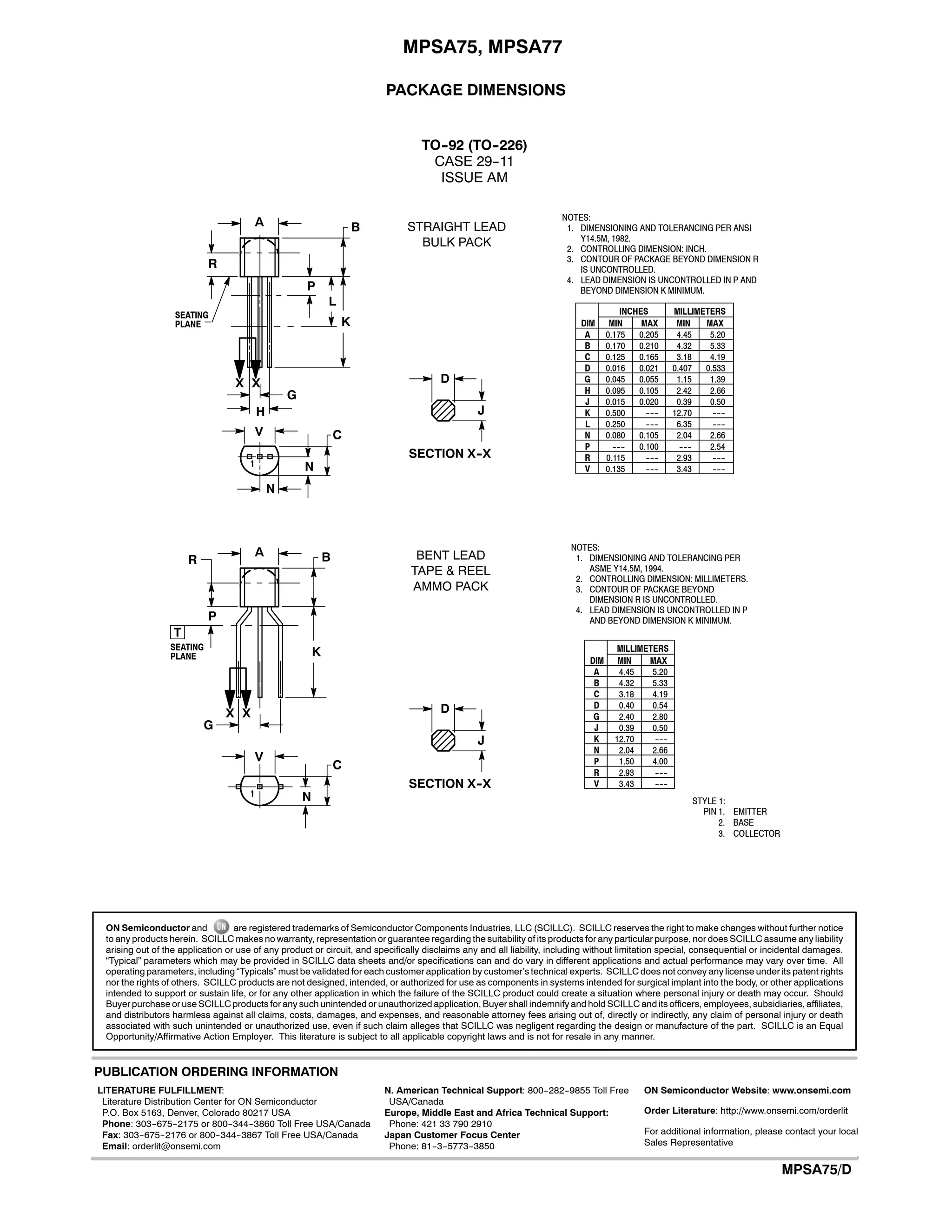
- Package dimensions and markings for the TO-92 package used by these transistors.