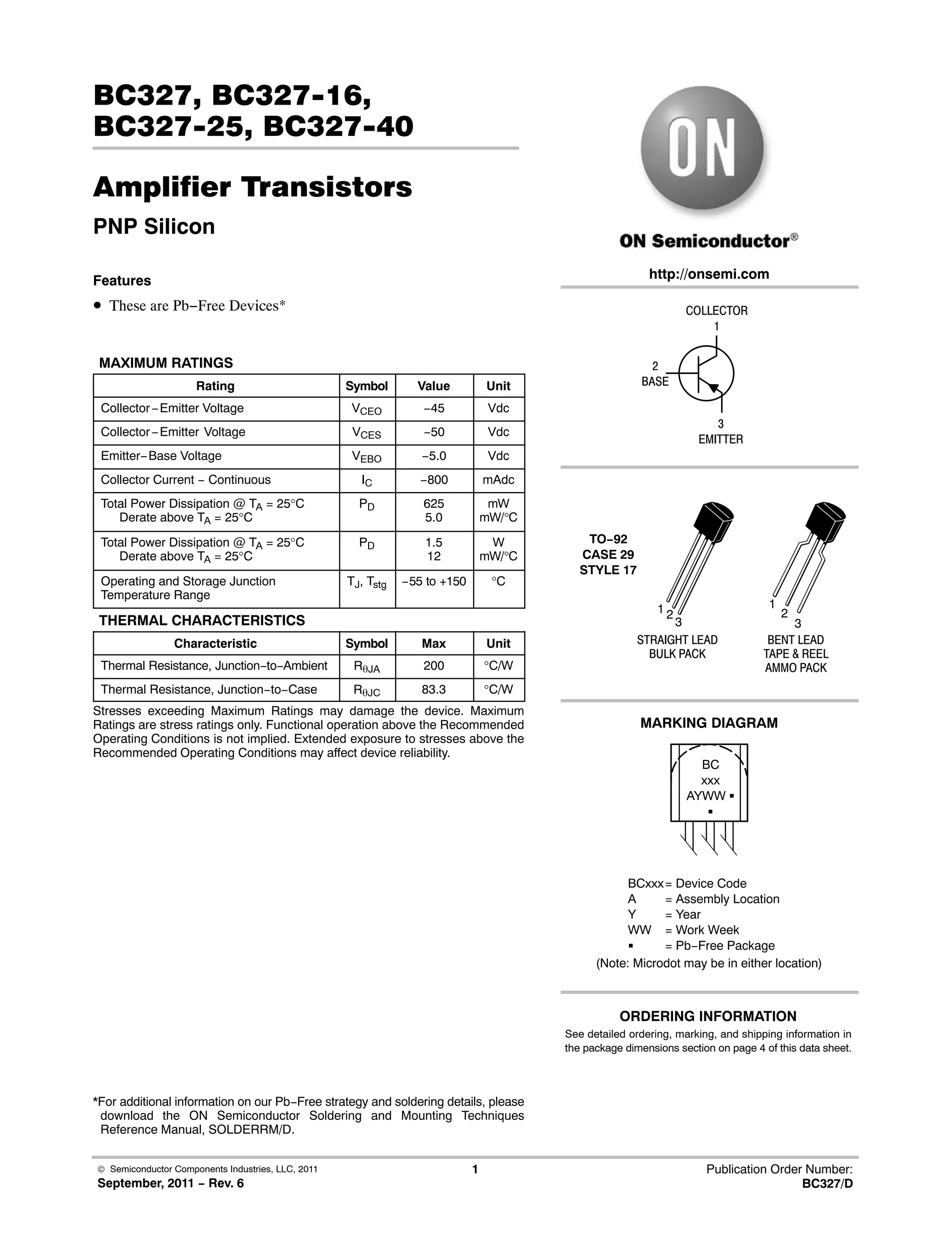
This document provides information on a series of PNP silicon amplifier transistors (BC327, BC327-16, BC327-25, BC327-40) from ON Semiconductor, including:
- Maximum ratings and characteristics like collector-emitter voltage, power dissipation, and thermal resistance.
- Electrical characteristics in active, saturation, and cutoff regions including current gain, voltage, and capacitance.
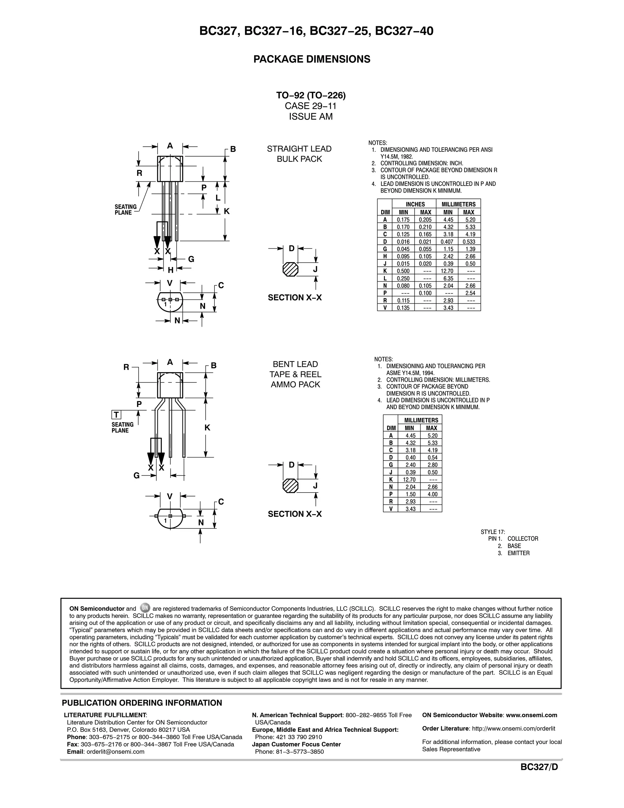
- Ordering information and package dimensions for the TO-92 package type.
- Graphs of characteristics like safe operating area, current gain vs. collector current, and capacitance vs. voltage/current.