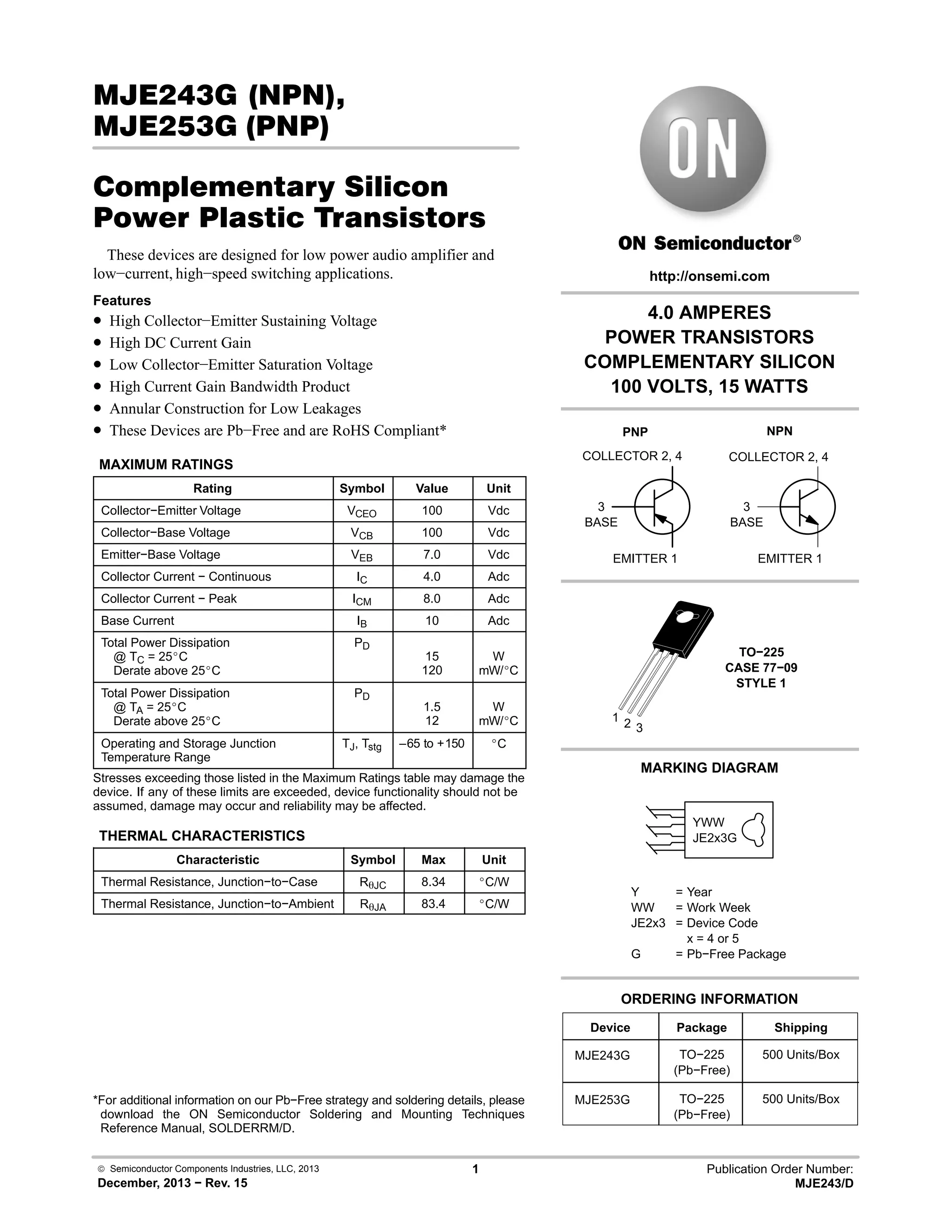
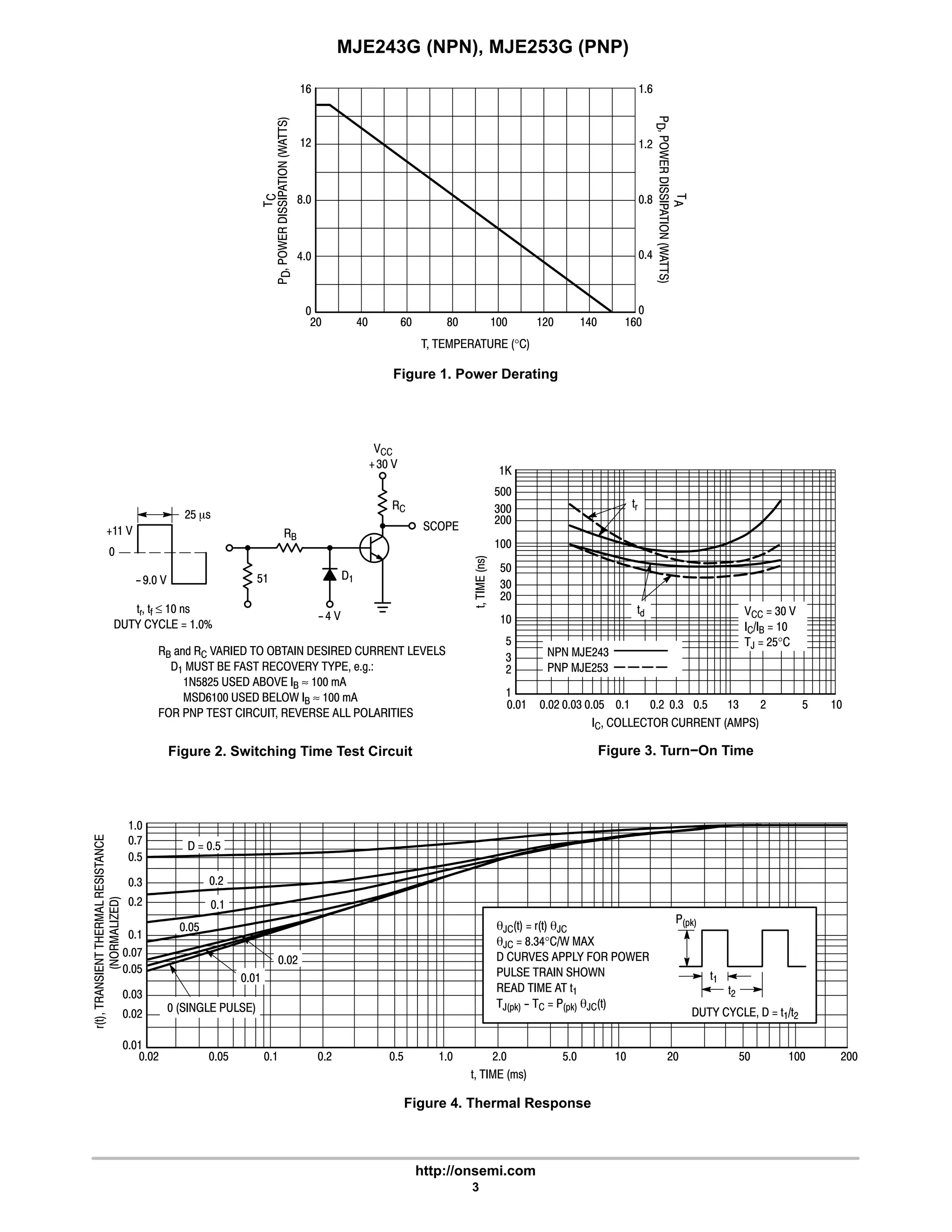
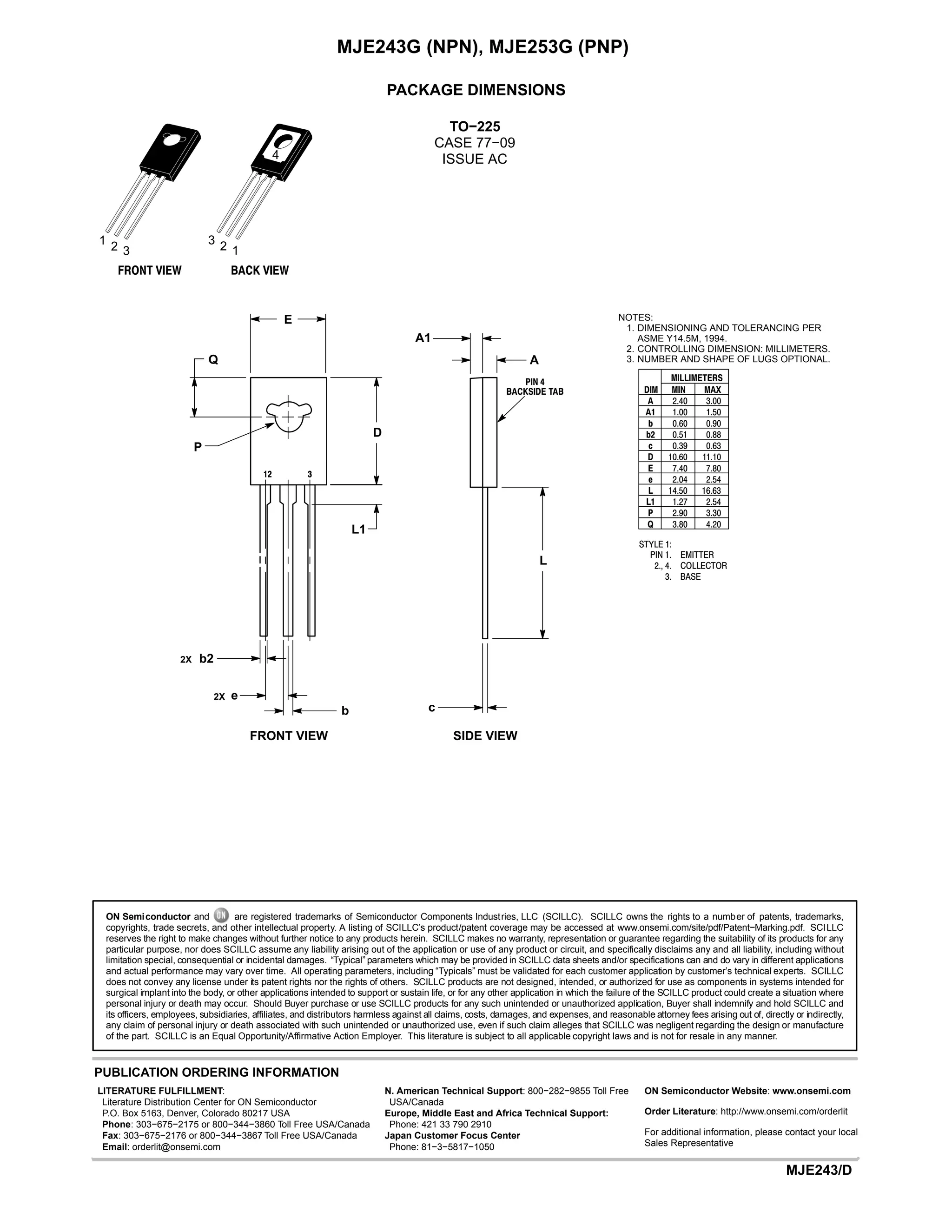
© Semiconductor Components Industries, LLC, 2013
December, 2013 − Rev. 15
1 Publication Order Number:
MJE243/D
MJE243G (NPN),
MJE253G (PNP)
Complementary Silicon
Power Plastic Transistors
These devices are designed for low power audio amplifier and
low−current, high−speed switching applications.
Features
• High Collector−Emitter Sustaining Voltage
• High DC Current Gain
• Low Collector−Emitter Saturation Voltage
• High Current Gain Bandwidth Product
• Annular Construction for Low Leakages
• These Devices are Pb−Free and are RoHS Compliant*
MAXIMUM RATINGS
Rating Symbol Value Unit
Collector−Emitter Voltage VCEO 100 Vdc
Collector−Base Voltage VCB 100 Vdc
Emitter−Base Voltage VEB 7.0 Vdc
Collector Current − Continuous IC 4.0 Adc
Collector Current − Peak ICM 8.0 Adc
Base Current IB 10 Adc
Total Power Dissipation
@ TC = 25_C
Derate above 25_C
PD
15
120
W
mW/_C
Total Power Dissipation
@ TA = 25_C
Derate above 25_C
PD
1.5
12
W
mW/_C
Operating and Storage Junction
Temperature Range
TJ, Tstg –65 to +150 _C
Stresses exceeding those listed in the Maximum Ratings table may damage the
device. If any of these limits are exceeded, device functionality should not be
assumed, damage may occur and reliability may be affected.
THERMAL CHARACTERISTICS
Characteristic Symbol Max Unit
Thermal Resistance, Junction−to−Case RqJC 8.34 _C/W
Thermal Resistance, Junction−to−Ambient RqJA 83.4 _C/W
*For additional information on our Pb−Free strategy and soldering details, please
download the ON Semiconductor Soldering and Mounting Techniques
Reference Manual, SOLDERRM/D.
Device Package Shipping
ORDERING INFORMATION
4.0 AMPERES
POWER TRANSISTORS
COMPLEMENTARY SILICON
100 VOLTS, 15 WATTS
http://onsemi.com
MJE243G TO−225
(Pb−Free)
500 Units/Box
MARKING DIAGRAM
Y = Year
WW = Work Week
JE2x3 = Device Code
x = 4 or 5
G = Pb−Free Package
MJE253G TO−225
(Pb−Free)
500 Units/Box
3
BASE
EMITTER 1
COLLECTOR 2, 4
3
BASE
EMITTER 1
COLLECTOR 2, 4
PNP NPN
TO−225
CASE 77−09
STYLE 1
1 2 3
YWW
JE2x3G
http://www.Datasheet4U.com
MJE243G (NPN), MJE253G (PNP)
http://onsemi.com
2
ELECTRICAL CHARACTERISTICS (TC = 25_C unless otherwise noted)
Characteristic Symbol Min Max Unit
OFF CHARACTERISTICS
Collector−Emitter Sustaining Voltage
(IC = 10 mAdc, IB = 0)
VCEO(sus)
100 −
V
Collector Cutoff Current
(VCB = 100 Vdc, IE = 0)
(VCE = 100 Vdc, IE = 0, TC = 125_C)
ICBO
−
−
0.1
0.1
mA
mA
Emitter Cutoff Current
(VBE = 7.0 Vdc, IC = 0)
IEBO
− 0.1
mAdc
ON CHARACTERISTICS
DC Current Gain
(IC = 200 mAdc, VCE = 1.0 Vdc)
(IC = 1.0 Adc, VCE = 1.0 Vdc)
hFE
40
15
180
−
−
Collector−Emitter Saturation Voltage
(IC = 500 mAdc, IB = 50 mAdc)
(IC = 1.0 Adc, IB = 100 mAdc)
VCE(sat)
−
−
0.3
0.6
V
Base−Emitter Saturation Voltage
(IC = 2.0 Adc, IB = 200 mAdc)
VBE(sat)
− 1.8
V
Base−Emitter On Voltage
(IC = 500 mAdc, VCE = 1.0 Vdc)
VBE(on)
− 1.5
V
DYNAMIC CHARACTERISTICS
Current−Gain − Bandwidth Product
(IC = 100 mAdc, VCE = 10 Vdc, ftest = 10 MHz)
fT
40 −
MHz
Output Capacitance
(VCB = 10 Vdc, IE = 0, f = 0.1 MHz)
Cob
− 50
pF
Product parametric performance is indicated in the Electrical Characteristics for the listed test conditions, unless otherwise noted. Product
performance may not be indicated by the Electrical Characteristics if operated under different conditions.
MJE243G (NPN), MJE253G (PNP)
http://onsemi.com
3
16
20
Figure 1. Power Derating
T, TEMPERATURE (°C)
0
40 60 100 120 160
12
PD,POWERDISSIPATION(WATTS)
1.6
0
1.2
8.0 0.8
4.0 0.4
80 140
TC
PD,POWERDISSIPATION(WATTS)
TA
Figure 2. Switching Time Test Circuit
+11 V
25 ms
0
- 9.0 V
RB
- 4 V
D1
SCOPE
VCC
+ 30 V
RC
tr, tf ≤ 10 ns
DUTY CYCLE = 1.0%
51
RB and RC VARIED TO OBTAIN DESIRED CURRENT LEVELS
 D1 MUST BE FAST RECOVERY TYPE, e.g.:
  1N5825 USED ABOVE IB ≈ 100 mA
  MSD6100 USED BELOW IB ≈ 100 mA
FOR PNP TEST CIRCUIT, REVERSE ALL POLARITIES
1K
IC, COLLECTOR CURRENT (AMPS)
VCC = 30 V
IC/IB = 10
TJ = 25°C
t,TIME(ns)
500
300
200
100
50
td
30
20
10
5
1
0.01 0.03 0.05 0.50.20.1 0.3 10
Figure 3. Turn−On Time
3
2
5213
tr
NPN MJE243
PNP MJE253
0.02
t, TIME (ms)
0.01
0.02 0.05 1.0 2.0 5.0 10 20 50 100 2000.1 0.50.2
1.0
0.2
0.1
0.05
r(t),TRANSIENTTHERMALRESISTANCE
qJC(t) = r(t) qJC
qJC = 8.34°C/W MAX
D CURVES APPLY FOR POWER
PULSE TRAIN SHOWN
READ TIME AT t1
TJ(pk) - TC = P(pk) qJC(t)
P(pk)
t1
t2
DUTY CYCLE, D = t1/t2
0.2
0 (SINGLE PULSE)
(NORMALIZED)
Figure 4. Thermal Response
0.5
D = 0.5
0.05
0.3
0.7
0.07
0.03
0.02
0.1
0.02
0.01
MJE243G (NPN), MJE253G (PNP)
http://onsemi.com
4
10
VCE, COLLECTOR-EMITTER VOLTAGE (VOLTS)
0.1
30
0.01
0.05
Figure 5. Active Region Safe Operating Area
500 ms
dc
5.0
20107.05.03.02.01.0
100 ms
TJ = 150°C
IC,COLLECTORCURRENT(AMP)
0.2
0.5
1.0
2.0
0.02
1.0 ms
1007050
5.0 ms
BONDING WIRE LIMITED
THERMALLY LIMITED @
TC = 25°C (SINGLE PULSE)
SECOND BREAKDOWN LIMITED
CURVES APPLY BELOW
 RATED VCEO
MJE243/MJE253
There are two limitations on the power handling ability of
a transistor: average junction temperature and second
breakdown. Safe operating area curves indicate I C −V CE
limits of the transistor that must be observed for reliable
operation; i.e., the transistor must not be subjected to greater
dissipation than the curves indicate.
The data of Figure 5 is based on T J(pk) = 150_C; TC is
variable depending on conditions. Second breakdown pulse
limits are valid for duty cycles to 10% provided T J(pk)
≤ 150_C. TJ(pk) may be calculated from the data in Figure 4.
At high case temperatures, thermal limitations will reduce
the power that can be handled to values less than the
limitations imposed by second breakdown.
10K
IC, COLLECTOR CURRENT (AMPS)
10
5K
3K
2K
1K
500
300
200
100
50
Figure 6. Turn−Off Time
t,TIME(ns)
30
20
0.01 0.03 0.05 0.50.20.02 0.1 0.3 105213
VCC = 30 V
IC/IB = 10
IB1 = IB2
TJ = 25°C
ts
tf
VR, REVERSE VOLTAGE (VOLTS)
10
100
100
200
50
Figure 7. Capacitance
70
5020107.05.03.01.0
C,CAPACITANCE(pF)
2.0
TJ = 25°C
Cib
Cob
MJE243 (NPN)
MJE253 (PNP)
30
NPN MJE243
PNP MJE253
20
7030
MJE243G (NPN), MJE253G (PNP)
http://onsemi.com
5
IC, COLLECTOR CURRENT (AMP)
IC, COLLECTOR CURRENT (AMP)IC, COLLECTOR CURRENT (AMP)
hFE,DCCURRENTGAIN
Figure 8. DC Current Gain
Figure 9. “On” Voltages
IC, COLLECTOR CURRENT (AMP)
200
500
0.06 0.1 0.4 4.00.04
100
70
50
20
0.2
IC, COLLECTOR CURRENT (AMP)
Figure 10. Temperature Coefficients
5.0
1.0 2.00.6
25°C
TJ = 150°C
- 55°C
0.04
IC, COLLECTOR CURRENT (AMP)
1.4
1.2
0.8
0.4
0
TJ = 25°C
V,VOLTAGE(VOLTS) NPN
MJE243
PNP
MJE253
100
200
70
50
30
20
2.0
hFE,DCCURRENTGAIN
25°C
TJ = 150°C
- 55°C
VCE = 1.0 V
VCE = 2.0 V
V,VOLTAGE(VOLTS)
VCE(sat)
VBE @ VCE = 1.0 V
qVB FOR VBE
0
TJ = 25°C
VBE(sat) @ IC/IB = 10
IC/IB = 10
VBE @ VCE = 1.0 V
V,TEMPERATURECOEFFICIENTS(mV/C)°θ
+ 2.5
+ 2.0
+ 1.5
+ 1.0
0
- 0.5
- 1.0
- 1.5
- 2.0
+ 0.5
- 2.5
*APPLIES FOR IC/IB ≤ hFE/3
25°C to 150°C
- 55°C to 25°C
25°C to 150°C
- 55°C to 25°C
V,TEMPERATURECOEFFICIENTS(mV/C)°θ
+ 2.5
+ 2.0
+ 1.5
+ 1.0
0
- 0.5
- 1.0
- 1.5
- 2.0
+ 0.5
- 2.5
*APPLIES FOR IC/IB ≤ hFE/3
25°C to 150°C
- 55°C to 25°C
25°C to 150°C
- 55°C to 25°C
VCE = 1.0 V
VCE = 2.0 V
7.0
10
30
300
0.06 0.1 0.4 4.00.2 1.0 2.00.6
0.04 0.06 0.1 0.4 4.00.2 1.0 2.00.6
0.06 0.1 0.4 4.00.04 0.2 1.0 2.00.6
0.04 0.06 0.1 0.4 4.00.2 1.0 2.00.6
0.04 0.06 0.1 0.4 4.00.2 1.0 2.00.6
1.0
0.6
0.2
1.4
1.2
0.8
0.4
1.0
0.6
0.2
3.0
5.0
7.0
10
5.0
IC/IB = 10
VCE(sat)
5.0
VBE(sat) @ IC/IB = 10
*qVC FOR VCE(sat)
qVB FOR VBE
*qVC FOR VCE(sat)
MJE243G (NPN), MJE253G (PNP)
http://onsemi.com
6
PACKAGE DIMENSIONS
TO−225
CASE 77−09
ISSUE AC
DIM MIN MAX
MILLIMETERS
D 10.60 11.10
E 7.40 7.80
A 2.40 3.00
b 0.60 0.90
P 2.90 3.30
L1 1.27 2.54
c 0.39 0.63
L 14.50 16.63
b2 0.51 0.88
Q 3.80 4.20
A1 1.00 1.50
e 2.04 2.54
E
12 3
NOTES:
1. DIMENSIONING AND TOLERANCING PER
ASME Y14.5M, 1994.
2. CONTROLLING DIMENSION: MILLIMETERS.
3. NUMBER AND SHAPE OF LUGS OPTIONAL.
2X
2X
Q
D
L1
P
b2
b
e
c
L
A1
A
FRONT VIEW BACK VIEW
FRONT VIEW SIDE VIEW
1 2 3
3 2 1
4
PIN 4
BACKSIDE TAB
STYLE 1:
PIN 1. EMITTER
2., 4. COLLECTOR
3. BASE
ON Semiconductor and are registered trademarks of Semiconductor Components Industries, LLC (SCILLC). SCILLC owns the rights to a number of patents, trademarks,
copyrights, trade secrets, and other intellectual property. A listing of SCILLC’s product/patent coverage may be accessed at www.onsemi.com/site/pdf/Patent−Marking.pdf. SCILLC
reserves the right to make changes without further notice to any products herein. SCILLC makes no warranty, representation or guarantee regarding the suitability of its products for any
particular purpose, nor does SCILLC assume any liability arising out of the application or use of any product or circuit, and specifically disclaims any and all liability, including without
limitation special, consequential or incidental damages. “Typical” parameters which may be provided in SCILLC data sheets and/or specifications can and do vary in different applications
and actual performance may vary over time. All operating parameters, including “Typicals” must be validated for each customer application by customer’s technical experts. SCILLC
does not convey any license under its patent rights nor the rights of others. SCILLC products are not designed, intended, or authorized for use as components in systems intended for
surgical implant into the body, or other applications intended to support or sustain life, or for any other application in which the failure of the SCILLC product could create a situation where
personal injury or death may occur. Should Buyer purchase or use SCILLC products for any such unintended or unauthorized application, Buyer shall indemnify and hold SCILLC and
its officers, employees, subsidiaries, affiliates, and distributors harmless against all claims, costs, damages, and expenses, and reasonable attorney fees arising out of, directly or indirectly,
any claim of personal injury or death associated with such unintended or unauthorized use, even if such claim alleges that SCILLC was negligent regarding the design or manufacture
of the part. SCILLC is an Equal Opportunity/Affirmative Action Employer. This literature is subject to all applicable copyright laws and is not for resale in any manner.
PUBLICATION ORDERING INFORMATION
N. American Technical Support: 800−282−9855 Toll Free
USA/Canada
Europe, Middle East and Africa Technical Support:
Phone: 421 33 790 2910
Japan Customer Focus Center
Phone: 81−3−5817−1050
MJE243/D
LITERATURE FULFILLMENT:
Literature Distribution Center for ON Semiconductor
P.O. Box 5163, Denver, Colorado 80217 USA
Phone: 303−675−2175 or 800−344−3860 Toll Free USA/Canada
Fax: 303−675−2176 or 800−344−3867 Toll Free USA/Canada
Email: orderlit@onsemi.com
ON Semiconductor Website: www.onsemi.com
Order Literature: http://www.onsemi.com/orderlit
For additional information, please contact your local
Sales Representative

Original transistor NPN MJE243 MJE243G JE243G TO 225 New

  • 1.
    © Semiconductor ComponentsIndustries, LLC, 2013 December, 2013 − Rev. 15 1 Publication Order Number: MJE243/D MJE243G (NPN), MJE253G (PNP) Complementary Silicon Power Plastic Transistors These devices are designed for low power audio amplifier and low−current, high−speed switching applications. Features • High Collector−Emitter Sustaining Voltage • High DC Current Gain • Low Collector−Emitter Saturation Voltage • High Current Gain Bandwidth Product • Annular Construction for Low Leakages • These Devices are Pb−Free and are RoHS Compliant* MAXIMUM RATINGS Rating Symbol Value Unit Collector−Emitter Voltage VCEO 100 Vdc Collector−Base Voltage VCB 100 Vdc Emitter−Base Voltage VEB 7.0 Vdc Collector Current − Continuous IC 4.0 Adc Collector Current − Peak ICM 8.0 Adc Base Current IB 10 Adc Total Power Dissipation @ TC = 25_C Derate above 25_C PD 15 120 W mW/_C Total Power Dissipation @ TA = 25_C Derate above 25_C PD 1.5 12 W mW/_C Operating and Storage Junction Temperature Range TJ, Tstg –65 to +150 _C Stresses exceeding those listed in the Maximum Ratings table may damage the device. If any of these limits are exceeded, device functionality should not be assumed, damage may occur and reliability may be affected. THERMAL CHARACTERISTICS Characteristic Symbol Max Unit Thermal Resistance, Junction−to−Case RqJC 8.34 _C/W Thermal Resistance, Junction−to−Ambient RqJA 83.4 _C/W *For additional information on our Pb−Free strategy and soldering details, please download the ON Semiconductor Soldering and Mounting Techniques Reference Manual, SOLDERRM/D. Device Package Shipping ORDERING INFORMATION 4.0 AMPERES POWER TRANSISTORS COMPLEMENTARY SILICON 100 VOLTS, 15 WATTS http://onsemi.com MJE243G TO−225 (Pb−Free) 500 Units/Box MARKING DIAGRAM Y = Year WW = Work Week JE2x3 = Device Code x = 4 or 5 G = Pb−Free Package MJE253G TO−225 (Pb−Free) 500 Units/Box 3 BASE EMITTER 1 COLLECTOR 2, 4 3 BASE EMITTER 1 COLLECTOR 2, 4 PNP NPN TO−225 CASE 77−09 STYLE 1 1 2 3 YWW JE2x3G http://www.Datasheet4U.com
  • 2.
    MJE243G (NPN), MJE253G(PNP) http://onsemi.com 2 ELECTRICAL CHARACTERISTICS (TC = 25_C unless otherwise noted) Characteristic Symbol Min Max Unit OFF CHARACTERISTICS Collector−Emitter Sustaining Voltage (IC = 10 mAdc, IB = 0) VCEO(sus) 100 − V Collector Cutoff Current (VCB = 100 Vdc, IE = 0) (VCE = 100 Vdc, IE = 0, TC = 125_C) ICBO − − 0.1 0.1 mA mA Emitter Cutoff Current (VBE = 7.0 Vdc, IC = 0) IEBO − 0.1 mAdc ON CHARACTERISTICS DC Current Gain (IC = 200 mAdc, VCE = 1.0 Vdc) (IC = 1.0 Adc, VCE = 1.0 Vdc) hFE 40 15 180 − − Collector−Emitter Saturation Voltage (IC = 500 mAdc, IB = 50 mAdc) (IC = 1.0 Adc, IB = 100 mAdc) VCE(sat) − − 0.3 0.6 V Base−Emitter Saturation Voltage (IC = 2.0 Adc, IB = 200 mAdc) VBE(sat) − 1.8 V Base−Emitter On Voltage (IC = 500 mAdc, VCE = 1.0 Vdc) VBE(on) − 1.5 V DYNAMIC CHARACTERISTICS Current−Gain − Bandwidth Product (IC = 100 mAdc, VCE = 10 Vdc, ftest = 10 MHz) fT 40 − MHz Output Capacitance (VCB = 10 Vdc, IE = 0, f = 0.1 MHz) Cob − 50 pF Product parametric performance is indicated in the Electrical Characteristics for the listed test conditions, unless otherwise noted. Product performance may not be indicated by the Electrical Characteristics if operated under different conditions.
  • 3.
    MJE243G (NPN), MJE253G(PNP) http://onsemi.com 3 16 20 Figure 1. Power Derating T, TEMPERATURE (°C) 0 40 60 100 120 160 12 PD,POWERDISSIPATION(WATTS) 1.6 0 1.2 8.0 0.8 4.0 0.4 80 140 TC PD,POWERDISSIPATION(WATTS) TA Figure 2. Switching Time Test Circuit +11 V 25 ms 0 - 9.0 V RB - 4 V D1 SCOPE VCC + 30 V RC tr, tf ≤ 10 ns DUTY CYCLE = 1.0% 51 RB and RC VARIED TO OBTAIN DESIRED CURRENT LEVELS  D1 MUST BE FAST RECOVERY TYPE, e.g.:   1N5825 USED ABOVE IB ≈ 100 mA   MSD6100 USED BELOW IB ≈ 100 mA FOR PNP TEST CIRCUIT, REVERSE ALL POLARITIES 1K IC, COLLECTOR CURRENT (AMPS) VCC = 30 V IC/IB = 10 TJ = 25°C t,TIME(ns) 500 300 200 100 50 td 30 20 10 5 1 0.01 0.03 0.05 0.50.20.1 0.3 10 Figure 3. Turn−On Time 3 2 5213 tr NPN MJE243 PNP MJE253 0.02 t, TIME (ms) 0.01 0.02 0.05 1.0 2.0 5.0 10 20 50 100 2000.1 0.50.2 1.0 0.2 0.1 0.05 r(t),TRANSIENTTHERMALRESISTANCE qJC(t) = r(t) qJC qJC = 8.34°C/W MAX D CURVES APPLY FOR POWER PULSE TRAIN SHOWN READ TIME AT t1 TJ(pk) - TC = P(pk) qJC(t) P(pk) t1 t2 DUTY CYCLE, D = t1/t2 0.2 0 (SINGLE PULSE) (NORMALIZED) Figure 4. Thermal Response 0.5 D = 0.5 0.05 0.3 0.7 0.07 0.03 0.02 0.1 0.02 0.01
  • 4.
    MJE243G (NPN), MJE253G(PNP) http://onsemi.com 4 10 VCE, COLLECTOR-EMITTER VOLTAGE (VOLTS) 0.1 30 0.01 0.05 Figure 5. Active Region Safe Operating Area 500 ms dc 5.0 20107.05.03.02.01.0 100 ms TJ = 150°C IC,COLLECTORCURRENT(AMP) 0.2 0.5 1.0 2.0 0.02 1.0 ms 1007050 5.0 ms BONDING WIRE LIMITED THERMALLY LIMITED @ TC = 25°C (SINGLE PULSE) SECOND BREAKDOWN LIMITED CURVES APPLY BELOW  RATED VCEO MJE243/MJE253 There are two limitations on the power handling ability of a transistor: average junction temperature and second breakdown. Safe operating area curves indicate I C −V CE limits of the transistor that must be observed for reliable operation; i.e., the transistor must not be subjected to greater dissipation than the curves indicate. The data of Figure 5 is based on T J(pk) = 150_C; TC is variable depending on conditions. Second breakdown pulse limits are valid for duty cycles to 10% provided T J(pk) ≤ 150_C. TJ(pk) may be calculated from the data in Figure 4. At high case temperatures, thermal limitations will reduce the power that can be handled to values less than the limitations imposed by second breakdown. 10K IC, COLLECTOR CURRENT (AMPS) 10 5K 3K 2K 1K 500 300 200 100 50 Figure 6. Turn−Off Time t,TIME(ns) 30 20 0.01 0.03 0.05 0.50.20.02 0.1 0.3 105213 VCC = 30 V IC/IB = 10 IB1 = IB2 TJ = 25°C ts tf VR, REVERSE VOLTAGE (VOLTS) 10 100 100 200 50 Figure 7. Capacitance 70 5020107.05.03.01.0 C,CAPACITANCE(pF) 2.0 TJ = 25°C Cib Cob MJE243 (NPN) MJE253 (PNP) 30 NPN MJE243 PNP MJE253 20 7030
  • 5.
    MJE243G (NPN), MJE253G(PNP) http://onsemi.com 5 IC, COLLECTOR CURRENT (AMP) IC, COLLECTOR CURRENT (AMP)IC, COLLECTOR CURRENT (AMP) hFE,DCCURRENTGAIN Figure 8. DC Current Gain Figure 9. “On” Voltages IC, COLLECTOR CURRENT (AMP) 200 500 0.06 0.1 0.4 4.00.04 100 70 50 20 0.2 IC, COLLECTOR CURRENT (AMP) Figure 10. Temperature Coefficients 5.0 1.0 2.00.6 25°C TJ = 150°C - 55°C 0.04 IC, COLLECTOR CURRENT (AMP) 1.4 1.2 0.8 0.4 0 TJ = 25°C V,VOLTAGE(VOLTS) NPN MJE243 PNP MJE253 100 200 70 50 30 20 2.0 hFE,DCCURRENTGAIN 25°C TJ = 150°C - 55°C VCE = 1.0 V VCE = 2.0 V V,VOLTAGE(VOLTS) VCE(sat) VBE @ VCE = 1.0 V qVB FOR VBE 0 TJ = 25°C VBE(sat) @ IC/IB = 10 IC/IB = 10 VBE @ VCE = 1.0 V V,TEMPERATURECOEFFICIENTS(mV/C)°θ + 2.5 + 2.0 + 1.5 + 1.0 0 - 0.5 - 1.0 - 1.5 - 2.0 + 0.5 - 2.5 *APPLIES FOR IC/IB ≤ hFE/3 25°C to 150°C - 55°C to 25°C 25°C to 150°C - 55°C to 25°C V,TEMPERATURECOEFFICIENTS(mV/C)°θ + 2.5 + 2.0 + 1.5 + 1.0 0 - 0.5 - 1.0 - 1.5 - 2.0 + 0.5 - 2.5 *APPLIES FOR IC/IB ≤ hFE/3 25°C to 150°C - 55°C to 25°C 25°C to 150°C - 55°C to 25°C VCE = 1.0 V VCE = 2.0 V 7.0 10 30 300 0.06 0.1 0.4 4.00.2 1.0 2.00.6 0.04 0.06 0.1 0.4 4.00.2 1.0 2.00.6 0.06 0.1 0.4 4.00.04 0.2 1.0 2.00.6 0.04 0.06 0.1 0.4 4.00.2 1.0 2.00.6 0.04 0.06 0.1 0.4 4.00.2 1.0 2.00.6 1.0 0.6 0.2 1.4 1.2 0.8 0.4 1.0 0.6 0.2 3.0 5.0 7.0 10 5.0 IC/IB = 10 VCE(sat) 5.0 VBE(sat) @ IC/IB = 10 *qVC FOR VCE(sat) qVB FOR VBE *qVC FOR VCE(sat)
  • 6.
    MJE243G (NPN), MJE253G(PNP) http://onsemi.com 6 PACKAGE DIMENSIONS TO−225 CASE 77−09 ISSUE AC DIM MIN MAX MILLIMETERS D 10.60 11.10 E 7.40 7.80 A 2.40 3.00 b 0.60 0.90 P 2.90 3.30 L1 1.27 2.54 c 0.39 0.63 L 14.50 16.63 b2 0.51 0.88 Q 3.80 4.20 A1 1.00 1.50 e 2.04 2.54 E 12 3 NOTES: 1. DIMENSIONING AND TOLERANCING PER ASME Y14.5M, 1994. 2. CONTROLLING DIMENSION: MILLIMETERS. 3. NUMBER AND SHAPE OF LUGS OPTIONAL. 2X 2X Q D L1 P b2 b e c L A1 A FRONT VIEW BACK VIEW FRONT VIEW SIDE VIEW 1 2 3 3 2 1 4 PIN 4 BACKSIDE TAB STYLE 1: PIN 1. EMITTER 2., 4. COLLECTOR 3. BASE ON Semiconductor and are registered trademarks of Semiconductor Components Industries, LLC (SCILLC). SCILLC owns the rights to a number of patents, trademarks, copyrights, trade secrets, and other intellectual property. A listing of SCILLC’s product/patent coverage may be accessed at www.onsemi.com/site/pdf/Patent−Marking.pdf. SCILLC reserves the right to make changes without further notice to any products herein. SCILLC makes no warranty, representation or guarantee regarding the suitability of its products for any particular purpose, nor does SCILLC assume any liability arising out of the application or use of any product or circuit, and specifically disclaims any and all liability, including without limitation special, consequential or incidental damages. “Typical” parameters which may be provided in SCILLC data sheets and/or specifications can and do vary in different applications and actual performance may vary over time. All operating parameters, including “Typicals” must be validated for each customer application by customer’s technical experts. SCILLC does not convey any license under its patent rights nor the rights of others. SCILLC products are not designed, intended, or authorized for use as components in systems intended for surgical implant into the body, or other applications intended to support or sustain life, or for any other application in which the failure of the SCILLC product could create a situation where personal injury or death may occur. Should Buyer purchase or use SCILLC products for any such unintended or unauthorized application, Buyer shall indemnify and hold SCILLC and its officers, employees, subsidiaries, affiliates, and distributors harmless against all claims, costs, damages, and expenses, and reasonable attorney fees arising out of, directly or indirectly, any claim of personal injury or death associated with such unintended or unauthorized use, even if such claim alleges that SCILLC was negligent regarding the design or manufacture of the part. SCILLC is an Equal Opportunity/Affirmative Action Employer. This literature is subject to all applicable copyright laws and is not for resale in any manner. PUBLICATION ORDERING INFORMATION N. American Technical Support: 800−282−9855 Toll Free USA/Canada Europe, Middle East and Africa Technical Support: Phone: 421 33 790 2910 Japan Customer Focus Center Phone: 81−3−5817−1050 MJE243/D LITERATURE FULFILLMENT: Literature Distribution Center for ON Semiconductor P.O. Box 5163, Denver, Colorado 80217 USA Phone: 303−675−2175 or 800−344−3860 Toll Free USA/Canada Fax: 303−675−2176 or 800−344−3867 Toll Free USA/Canada Email: orderlit@onsemi.com ON Semiconductor Website: www.onsemi.com Order Literature: http://www.onsemi.com/orderlit For additional information, please contact your local Sales Representative