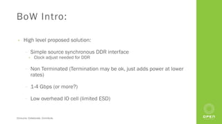
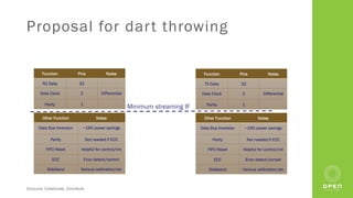
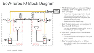
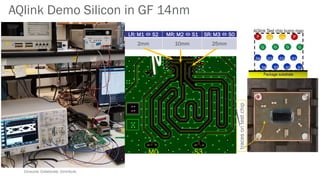
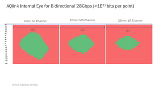
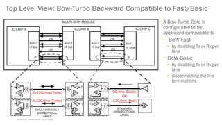
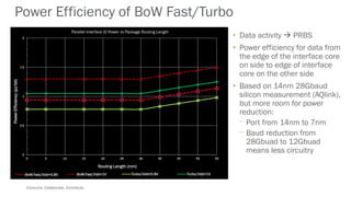
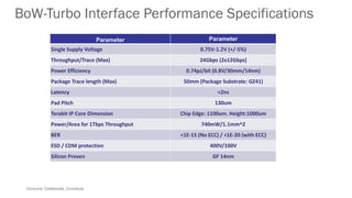
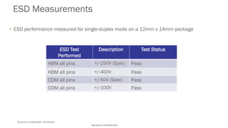
Consume. Collaborate. Contribute.Consume. Collaborate. Contribute.
BoW: Basic, Fast, Turbo
Die-to-Die Open Interface Solutions
ODSA Project Workshop Mark Kuemerle
March 28, 2019 Ramin Farjad
Consume. Collaborate. Contribute.
Interface standardization
• Chiplet based systems will likely have a variety of different interfaces
moving forward
⎻ Fast Serial interfaces with some compatibility to existing standards
(eg 112GXSR)
⎻ Novel USR interfaces driven by an ecosystem (eg. Kandou/Marvell)
⎻ Simple interfaces for moving reasonable bandwidth between die
from less cutting edge nodes
Consume. Collaborate. Contribute.
Does it make sense?
• Does it make sense to have another parallel standard?
⎻ AIB is a good starting point, currently has datarate and footprint
definitions that limit use on a laminate
⎻ Making the spec as open as possible can hopefully speed up
useability
• How do we decide if this effort is providing a value to the community?
⎻ Inertia from participants, adoption in products
• Standardization coalesces
• Adoption in custom/’contained’ interfaces
• Moving to interoperable interfaces between various die
Consume. Collaborate. Contribute.
The basic idea
• Blast from the past – use simple CMOS IO to
communicate
• We stopped using these when SERDES simplified
board routing (less traces=less $$)
• Keeping everything on a laminate keeps things simple
⎻ More routing traces than a board
⎻ Less ESD requirements
• Make an interface that works on a cheap laminate or a
fancy silicon based interconnect
⎻ Enable compatibility where we can
Consume. Collaborate. Contribute.
BoW Intro:
• High level proposed solution:
⎻ Simple source synchronous DDR interface
• Clock adjust needed for DDR
⎻ Non Terminated (Termination may be ok, just adds power at lower
rates)
⎻ 1-4 Gbps (or more?)
⎻ Low overhead IO cell (limited ESD)
Consume. Collaborate. Contribute.
BoW Extensions:
• Data Integrity / Power functions – need to discuss
⎻ ECC – How critical is BER? How much does interface spend vs.
⎻ DBI – is power worth the pins?
• Extension Mode 2: Bow-Fast
⎻ Higher speed uses optional termination (~2-3x rate), minor impact
on power
• Extension Mode 3: Bow-Turbo
⎻ Add potential bidirectional feature – implemented in the IO cell
• Hybrid circuit – can be implemented in multiple ways (examples from BaseT)
Consume. Collaborate. Contribute.
Proposal for dart throwing
Function Pins Notes
RX Data 32
Data Clock 2 Differential
Parity 1
Other Function Notes
Data Bus Inversion ~19% power savings
Parity Not needed if ECC
FIFO Reset Helpful for control/init
ECC Error detect/correct
Sideband Various calibration/etc
Function Pins Notes
TX Data 32
Data Clock 2 Differential
Parity 1
Other Function Notes
Data Bus Inversion ~19% power savings
Parity Not needed if ECC
FIFO Reset Helpful for control/init
ECC Error detect/correct
Sideband Various calibration/etc
Minimum streaming IF
Consume. Collaborate. Contribute.
Datarate discussion
• Current proposal: Per databit wire configurable from 1-4Gbps
• What datarates make the most sense for the standard?
⎻ 1-2Gbps (AHB) limits usefulness on laminate (too many wires to move
reasonable bandwidth
⎻ Configurable datarate including 1-2 Gbps could enable AHB
compatibility
⎻ >5Gbps may require termination
• Having a settable datarate with simple divides maximizes compatibility
⎻ For 4, 2, 1 Gbps -> simple dividers
Consume. Collaborate. Contribute.
Voltage discussion
• Simple, single voltage based approach – challenge is what
voltage to choose?
• 1.2 is HBM legacy, costs power
• 0.9V is often available, decent power, interoperable with AIB*
• 0.75 / 0.8 often available as well, popular chiplevel VDD values
• Lower voltages will have lower power, too low will be a challenge
for IO design
Consume. Collaborate. Contribute.
Power (energy)
• Simple energy calculation
⎻ Pathological worst case w/DBI
• 0.4
⎻ No on chip routing from IO to
bump assumed
• Add 0.1 – 0.25 pJ depending on
length
⎻ Termination +~0.2 pJ low
speed, less at high speed
0.00
0.50
1.00
1.50
2.00
2.50
3.00
3.50
4.00
4.50
0 5 10 15 20 25 30 35 40 45 50
PowerpJ/bit
Routing Length (mm)
Parallel Interface IO Power vs Package Routing Length
Total power at 1.2V Total power at 1.0V Total power at 0.8V
Consume. Collaborate. Contribute.
• BOW Basic
⎻ Unterminated lanes  up to 5 Gbps/wire
⎻ Source Synchronous with clock alignment
• BOW Fast
⎻ Terminated lanes  up to 12Gbps/wire
⎻ Source Synchronous with clock alignment
• BOW Turbo
⎻ Simultaneous Bidirectional  both directions
⎻ Terminated lanes  up to 2x12Gbps/wire
⎻ Source Synchronous with clock alignment
Note: Bidirectional signaling been around for decades, in all phone
lines, and at multi-Gig in BASE-T PHYs since late 1990s. The
cancellation requirement for a link with small loss is fairly relaxed
Operation Modes BoW on Organic Package Substrate
Tx/RxTx/Rx
Tx/Rx Tx/Rx
Transmit/Receive data
RxTx
Rx Tx
Transmit data
Receive data
RxTx
Rx Tx
Transmit data
Receive data
Terminated Transmission Lines
Unterminated Wires
Consume. Collaborate. Contribute.
BoW-Turbo IO Block Diagram
Hybrid
Zo
Zo
Hybrid
TxTx
Rx Rx
• A Hybrid block, placed between the pad
and basic BoW Tx/Rx ports, creates a
Bow Turbo port
⎻ Passes local Tx output signal to the IO pad
⎻ Subtracts local Tx output signal from the
combined signal on IO pas and passes the
resulting signal to Rx input
⎻ Once implemented, Easy to port
• BoW-Turbo is backward compatible with
Bow-Basic & BoW-Fast
⎻ Interface can easily be programed to act as a
transmit only or receive only port
• Total area for BoW-Turbo transceiver is
<0.018mm2.
⎻ Can be integrated under single pad area (pad
pitch=130um)
• Bow-Turbo concept proven in Silicon
⎻ AQlink SerDes in GF 14nm operated in Single-
ended mode
BoW-Turbo BoW-Turbo
Consume. Collaborate. Contribute.
AQlink Demo Silicon in GF 14nm
M0M1M2M3
LR: M1  S2 MR: M2  S1 SR: M3  S0
2mm 10mm 25mm
M0 S3
tracesontestchip
Consume. Collaborate. Contribute.
AQlink External Ports
External Eye
@28Gbps
• One port per AQlink Quad core is an
external port. Each external port trace:
⎻ 10mm package
⎻ 30mm board (1/2 package loss)
Effective 10+15=~25mm package
Loopback trace=2x25=50mm
• A differential external loop back
operates error free up to ~25Gbps per
direction (BER~1E-15)
• If loopback connected in single-ended
fashion, the link operates error free
up to ~15Gbps/direction (BER~1E-15)
• To provide further margin, simplify the
phase alignment & duty cycle
corrector, maximum Bow-Turbo speed
limited to 12Gbps/direction
Consume. Collaborate. Contribute.
AQlink Internal Eye for Bidirectional 28Gbps (>1E11 bits per point)
2mm: SR Channel 10mm: MR Channel 25mm: LR Channel
1UI 1UI 1UI
Consume. Collaborate. Contribute.
Top Level View: Bow-Turbo Backward Compatible to Fast/Basic
clk
clk
clk
clk
5G/line (Basic)
OR
12G/line (Fast)
2x12G/line (Turbo)
• A Bow-Turbo Core is
configurable to be
backward compatible to
⎻ BoW-Fast
• by disabling Tx or Rx per
lane
⎻ BoW-Basic
• by disabling Tx or Rx per
lane
• disconnecting the line
terminations
2x12G/line (Turbo)
Consume. Collaborate. Contribute.
~1000um
~1100um (Bump Pitch=130um)
S13
S5
S14
S6
S15
S7
S16
S8
Ck-
S9
S1
S10
S2
S11
S3
S12
S4
Sample BoW Staggered Bump Map – Terabit Core
GP PGP P G G
S13
S5
S14
S6
S15
S7
S16
S8
S9
S1
S10
S2
S11
S3
S12
S4
S5 S6 S7 S8S1 S2 S3 S4
S13 S14 S15 S16S9 S10 S11 S12
Ck+
Ck-
Ck+
• Terabit Module has 48 data pads:
⎻ 48x2x11.5Gbps/pad=1Tbps/mm
• A common bump map can be used
for Basic/Fast/Turbo
⎻ Important for backward compatibility
• Two clock ports per 16 data ports
⎻ Configurable to be clock output or clock
input pads when connected to non-Turbo
interface (Tx or Rx only)
• Optional ECC
⎻ Option column to add one ECC bit per 16
data group at the edge of the Terabit Core
bump map to provide error correction
capability if BER<1E-20
Ck-
Ck+
E0
E0
E0
GP PGP P G G
GP PGP P G G
G
G
P
Consume. Collaborate. Contribute.
• Data activity  PRBS
• Power efficiency for data from
the edge of the interface core
on side to edge of interface
core on the other side
• Based on 14nm 28Gbaud
silicon measurement (AQlink),
but more room for power
reduction:
⎻ Port from 14nm to 7nm
⎻ Baud reduction from
28Gbuad to 12Gbuad
means less circuitry
Power Efficiency of BoW Fast/Turbo
0
0.5
1
1.5
2
0 5 10 15 20 25 30 35 40 45 50
Parallel Interface IO Power vs Package Routing Length
Routing Length (mm)
PowerEfficiency(pJ/bit)
BoW.Fast/Vdd=0.8V BoW.Fast/Vdd=1V Turbo/Vdd=0.8V Turbo/Vdd=1V
Consume. Collaborate. Contribute.
BoW-Turbo Interface Performance Specifications
Parameter Parameter
Single Supply Voltage 0.75V-1.2V (+/-5%)
Throughput/Trace (Max) 24Gbps (2x12Gbps)
Power Efficiency 0.74pJ/bit (0.8V/30mm/14nm)
Package Trace length (Max) 50mm (Package Substrate: GZ41)
Latency <2ns
Pad Pitch 130um
Terabit IP Core Dimension Chip Edge: 1100um. Height:1000um
Power/Area for 1Tbps Throughput 740mW/1.1mm^2
BER <1E-15 (No ECC) / <1E-20 (with ECC)
ESD / CDM protection 400V/100V
Silicon Proven GF 14nm
Consume. Collaborate. Contribute.
BoW Turbo Spec Summary
• Over 1Tbps/mm chip edge over organic substrate & 130um pad pitch
• Throughput per port of 2x10.5Gbps (up to: 2x12Gbps)
• Small per port area of <0.018mm2
• Less than 1pJ/bit in 14nm at Vdd=0.8V and trace=50mm
• Single power supply that is compatible with synthesized logic core
• Concept proven in 14nm Silicon (Hybrid easy to port to other nodes)
• Easy and quick to port into other process nodes (Just a 10G USR)
• Backward compatible with BoW Basic/Fast die-die interfaces
• Can use matching bump map as Bow Basic/Fast
• A Chiplet with Bow Turbo interoperates with all Chiplets using other BoW interfaces
Consume. Collaborate. Contribute.
Test Options
• Need discussion to find suitable test solutions
⎻ Calibration?
⎻ 1149.1 legacy (JTAG scan)
⎻ IEEE 1500 (HBM type systems)
⎻ Could define at speed / functional interop test if needed
Consume. Collaborate. Contribute.
Call for Volunteers
• We need your help to define a generally useful and interoperable
interface
• What do we need?
⎻ Good ideas on what applications the BoW makes sense for
⎻ SI/PI input for various options
⎻ Defining test for interface
Consume. Collaborate. Contribute.
Thank You
Consume. Collaborate. Contribute.
AQlink Measured Power Efficiency (Quad) TT15 part
Nominal Vdd range = 0.75V - 0.85V (+/-3% tolerance)
Consume. Collaborate. Contribute.
25Gbps
AQlink External Eye Diagrams
28Gbps
Consume. Collaborate. Contribute.
• ESD performance measured for single-duplex mode on a 12mm x 14mm package
ESD Test
Performed
Description Test Status
HBM all pins +/-250V (Spec) Pass
HBM all pins +/-400V Pass
CDM all pins +/-50V (Spec) Pass
CDM all pins +/-100V Pass
ESD Measurements
Aquantia Confidential

ODSA BoW: Basic, Fast, Turbo Die to Die Open Interface Solutions

  • 1.
    Consume. Collaborate. Contribute.Consume.Collaborate. Contribute. BoW: Basic, Fast, Turbo Die-to-Die Open Interface Solutions ODSA Project Workshop Mark Kuemerle March 28, 2019 Ramin Farjad
  • 2.
    Consume. Collaborate. Contribute. Interfacestandardization • Chiplet based systems will likely have a variety of different interfaces moving forward ⎻ Fast Serial interfaces with some compatibility to existing standards (eg 112GXSR) ⎻ Novel USR interfaces driven by an ecosystem (eg. Kandou/Marvell) ⎻ Simple interfaces for moving reasonable bandwidth between die from less cutting edge nodes
  • 3.
    Consume. Collaborate. Contribute. Doesit make sense? • Does it make sense to have another parallel standard? ⎻ AIB is a good starting point, currently has datarate and footprint definitions that limit use on a laminate ⎻ Making the spec as open as possible can hopefully speed up useability • How do we decide if this effort is providing a value to the community? ⎻ Inertia from participants, adoption in products • Standardization coalesces • Adoption in custom/’contained’ interfaces • Moving to interoperable interfaces between various die
  • 4.
    Consume. Collaborate. Contribute. Thebasic idea • Blast from the past – use simple CMOS IO to communicate • We stopped using these when SERDES simplified board routing (less traces=less $$) • Keeping everything on a laminate keeps things simple ⎻ More routing traces than a board ⎻ Less ESD requirements • Make an interface that works on a cheap laminate or a fancy silicon based interconnect ⎻ Enable compatibility where we can
  • 5.
    Consume. Collaborate. Contribute. BoWIntro: • High level proposed solution: ⎻ Simple source synchronous DDR interface • Clock adjust needed for DDR ⎻ Non Terminated (Termination may be ok, just adds power at lower rates) ⎻ 1-4 Gbps (or more?) ⎻ Low overhead IO cell (limited ESD)
  • 6.
    Consume. Collaborate. Contribute. BoWExtensions: • Data Integrity / Power functions – need to discuss ⎻ ECC – How critical is BER? How much does interface spend vs. ⎻ DBI – is power worth the pins? • Extension Mode 2: Bow-Fast ⎻ Higher speed uses optional termination (~2-3x rate), minor impact on power • Extension Mode 3: Bow-Turbo ⎻ Add potential bidirectional feature – implemented in the IO cell • Hybrid circuit – can be implemented in multiple ways (examples from BaseT)
  • 7.
    Consume. Collaborate. Contribute. Proposalfor dart throwing Function Pins Notes RX Data 32 Data Clock 2 Differential Parity 1 Other Function Notes Data Bus Inversion ~19% power savings Parity Not needed if ECC FIFO Reset Helpful for control/init ECC Error detect/correct Sideband Various calibration/etc Function Pins Notes TX Data 32 Data Clock 2 Differential Parity 1 Other Function Notes Data Bus Inversion ~19% power savings Parity Not needed if ECC FIFO Reset Helpful for control/init ECC Error detect/correct Sideband Various calibration/etc Minimum streaming IF
  • 8.
    Consume. Collaborate. Contribute. Dataratediscussion • Current proposal: Per databit wire configurable from 1-4Gbps • What datarates make the most sense for the standard? ⎻ 1-2Gbps (AHB) limits usefulness on laminate (too many wires to move reasonable bandwidth ⎻ Configurable datarate including 1-2 Gbps could enable AHB compatibility ⎻ >5Gbps may require termination • Having a settable datarate with simple divides maximizes compatibility ⎻ For 4, 2, 1 Gbps -> simple dividers
  • 9.
    Consume. Collaborate. Contribute. Voltagediscussion • Simple, single voltage based approach – challenge is what voltage to choose? • 1.2 is HBM legacy, costs power • 0.9V is often available, decent power, interoperable with AIB* • 0.75 / 0.8 often available as well, popular chiplevel VDD values • Lower voltages will have lower power, too low will be a challenge for IO design
  • 10.
    Consume. Collaborate. Contribute. Power(energy) • Simple energy calculation ⎻ Pathological worst case w/DBI • 0.4 ⎻ No on chip routing from IO to bump assumed • Add 0.1 – 0.25 pJ depending on length ⎻ Termination +~0.2 pJ low speed, less at high speed 0.00 0.50 1.00 1.50 2.00 2.50 3.00 3.50 4.00 4.50 0 5 10 15 20 25 30 35 40 45 50 PowerpJ/bit Routing Length (mm) Parallel Interface IO Power vs Package Routing Length Total power at 1.2V Total power at 1.0V Total power at 0.8V
  • 11.
    Consume. Collaborate. Contribute. •BOW Basic ⎻ Unterminated lanes  up to 5 Gbps/wire ⎻ Source Synchronous with clock alignment • BOW Fast ⎻ Terminated lanes  up to 12Gbps/wire ⎻ Source Synchronous with clock alignment • BOW Turbo ⎻ Simultaneous Bidirectional  both directions ⎻ Terminated lanes  up to 2x12Gbps/wire ⎻ Source Synchronous with clock alignment Note: Bidirectional signaling been around for decades, in all phone lines, and at multi-Gig in BASE-T PHYs since late 1990s. The cancellation requirement for a link with small loss is fairly relaxed Operation Modes BoW on Organic Package Substrate Tx/RxTx/Rx Tx/Rx Tx/Rx Transmit/Receive data Transmit/Receive data RxTx Rx Tx Transmit data Receive data RxTx Rx Tx Transmit data Receive data Terminated Transmission Lines Terminated Transmission Lines Unterminated Wires
  • 12.
    Consume. Collaborate. Contribute. BoW-TurboIO Block Diagram Hybrid Zo Zo Hybrid TxTx Rx Rx • A Hybrid block, placed between the pad and basic BoW Tx/Rx ports, creates a Bow Turbo port ⎻ Passes local Tx output signal to the IO pad ⎻ Subtracts local Tx output signal from the combined signal on IO pas and passes the resulting signal to Rx input ⎻ Once implemented, Easy to port • BoW-Turbo is backward compatible with Bow-Basic & BoW-Fast ⎻ Interface can easily be programed to act as a transmit only or receive only port • Total area for BoW-Turbo transceiver is <0.018mm2. ⎻ Can be integrated under single pad area (pad pitch=130um) • Bow-Turbo concept proven in Silicon ⎻ AQlink SerDes in GF 14nm operated in Single- ended mode BoW-Turbo BoW-Turbo
  • 13.
    Consume. Collaborate. Contribute. AQlinkDemo Silicon in GF 14nm M0M1M2M3 LR: M1  S2 MR: M2  S1 SR: M3  S0 2mm 10mm 25mm M0 S3 tracesontestchip
  • 14.
    Consume. Collaborate. Contribute. AQlinkExternal Ports External Eye @28Gbps • One port per AQlink Quad core is an external port. Each external port trace: ⎻ 10mm package ⎻ 30mm board (1/2 package loss) Effective 10+15=~25mm package Loopback trace=2x25=50mm • A differential external loop back operates error free up to ~25Gbps per direction (BER~1E-15) • If loopback connected in single-ended fashion, the link operates error free up to ~15Gbps/direction (BER~1E-15) • To provide further margin, simplify the phase alignment & duty cycle corrector, maximum Bow-Turbo speed limited to 12Gbps/direction
  • 15.
    Consume. Collaborate. Contribute. AQlinkInternal Eye for Bidirectional 28Gbps (>1E11 bits per point) 2mm: SR Channel 10mm: MR Channel 25mm: LR Channel 1UI 1UI 1UI
  • 16.
    Consume. Collaborate. Contribute. TopLevel View: Bow-Turbo Backward Compatible to Fast/Basic clk clk clk clk 5G/line (Basic) OR 12G/line (Fast) 2x12G/line (Turbo) • A Bow-Turbo Core is configurable to be backward compatible to ⎻ BoW-Fast • by disabling Tx or Rx per lane ⎻ BoW-Basic • by disabling Tx or Rx per lane • disconnecting the line terminations 2x12G/line (Turbo)
  • 17.
    Consume. Collaborate. Contribute. ~1000um ~1100um(Bump Pitch=130um) S13 S5 S14 S6 S15 S7 S16 S8 Ck- S9 S1 S10 S2 S11 S3 S12 S4 Sample BoW Staggered Bump Map – Terabit Core GP PGP P G G S13 S5 S14 S6 S15 S7 S16 S8 S9 S1 S10 S2 S11 S3 S12 S4 S5 S6 S7 S8S1 S2 S3 S4 S13 S14 S15 S16S9 S10 S11 S12 Ck+ Ck- Ck+ • Terabit Module has 48 data pads: ⎻ 48x2x11.5Gbps/pad=1Tbps/mm • A common bump map can be used for Basic/Fast/Turbo ⎻ Important for backward compatibility • Two clock ports per 16 data ports ⎻ Configurable to be clock output or clock input pads when connected to non-Turbo interface (Tx or Rx only) • Optional ECC ⎻ Option column to add one ECC bit per 16 data group at the edge of the Terabit Core bump map to provide error correction capability if BER<1E-20 Ck- Ck+ E0 E0 E0 GP PGP P G G GP PGP P G G G G P
  • 18.
    Consume. Collaborate. Contribute. •Data activity  PRBS • Power efficiency for data from the edge of the interface core on side to edge of interface core on the other side • Based on 14nm 28Gbaud silicon measurement (AQlink), but more room for power reduction: ⎻ Port from 14nm to 7nm ⎻ Baud reduction from 28Gbuad to 12Gbuad means less circuitry Power Efficiency of BoW Fast/Turbo 0 0.5 1 1.5 2 0 5 10 15 20 25 30 35 40 45 50 Parallel Interface IO Power vs Package Routing Length Routing Length (mm) PowerEfficiency(pJ/bit) BoW.Fast/Vdd=0.8V BoW.Fast/Vdd=1V Turbo/Vdd=0.8V Turbo/Vdd=1V
  • 19.
    Consume. Collaborate. Contribute. BoW-TurboInterface Performance Specifications Parameter Parameter Single Supply Voltage 0.75V-1.2V (+/-5%) Throughput/Trace (Max) 24Gbps (2x12Gbps) Power Efficiency 0.74pJ/bit (0.8V/30mm/14nm) Package Trace length (Max) 50mm (Package Substrate: GZ41) Latency <2ns Pad Pitch 130um Terabit IP Core Dimension Chip Edge: 1100um. Height:1000um Power/Area for 1Tbps Throughput 740mW/1.1mm^2 BER <1E-15 (No ECC) / <1E-20 (with ECC) ESD / CDM protection 400V/100V Silicon Proven GF 14nm
  • 20.
    Consume. Collaborate. Contribute. BoWTurbo Spec Summary • Over 1Tbps/mm chip edge over organic substrate & 130um pad pitch • Throughput per port of 2x10.5Gbps (up to: 2x12Gbps) • Small per port area of <0.018mm2 • Less than 1pJ/bit in 14nm at Vdd=0.8V and trace=50mm • Single power supply that is compatible with synthesized logic core • Concept proven in 14nm Silicon (Hybrid easy to port to other nodes) • Easy and quick to port into other process nodes (Just a 10G USR) • Backward compatible with BoW Basic/Fast die-die interfaces • Can use matching bump map as Bow Basic/Fast • A Chiplet with Bow Turbo interoperates with all Chiplets using other BoW interfaces
  • 21.
    Consume. Collaborate. Contribute. TestOptions • Need discussion to find suitable test solutions ⎻ Calibration? ⎻ 1149.1 legacy (JTAG scan) ⎻ IEEE 1500 (HBM type systems) ⎻ Could define at speed / functional interop test if needed
  • 22.
    Consume. Collaborate. Contribute. Callfor Volunteers • We need your help to define a generally useful and interoperable interface • What do we need? ⎻ Good ideas on what applications the BoW makes sense for ⎻ SI/PI input for various options ⎻ Defining test for interface
  • 23.
  • 24.
    Consume. Collaborate. Contribute. AQlinkMeasured Power Efficiency (Quad) TT15 part Nominal Vdd range = 0.75V - 0.85V (+/-3% tolerance)
  • 25.
  • 26.
    Consume. Collaborate. Contribute. •ESD performance measured for single-duplex mode on a 12mm x 14mm package ESD Test Performed Description Test Status HBM all pins +/-250V (Spec) Pass HBM all pins +/-400V Pass CDM all pins +/-50V (Spec) Pass CDM all pins +/-100V Pass ESD Measurements Aquantia Confidential