Download to read offline
![IJRET: International Journal of Research in Engineering and Technology eISSN: 2319-1163 | pISSN: 2321-7308
__________________________________________________________________________________________
Volume: 02 Issue: 12 | Dec-2013, Available @ http://www.ijret.org 173
NOVEL TECHNIQUE IN CHARACTARIZING A PV MODULE USING
PULSE WIDTH MODULATOR
I.M. Mahmoud1
, S. O. Abdellatif2
, T. S. Abdelsalam3,4
,O. E. Abdellatif5
1
Teaching Assistant, E E. Department, The British University in Egypt, Cairo, Egypt
2
Assistant Lecturer, E E. Department, The British University in Egypt, Cairo, Egypt
3
Head of Department, E E. Department, The British University in Egypt, Cairo, Egypt
4
Assoc. Professor, Electrical Power and Machines Department, Ain Shams University, Cairo, Egypt
5
Professor, Mechanical Engineering Department, Banha University, Cairo, Egypt
Abstract
The fabrication and characterization of PV modules are always done under standard test conditions (STC). However, The condition of
operation are often far from thisstandard conditions. As a result, developing a characterization circuit is considered as a point of
interest for researchers.This paper presents a new methodology in characterizing a PV module using an electronic load circuit. The
circuit is implemented using a power MOSFET driven by a pulse width modulator (PWM) developed by LABVIEW. The system is
tested and its results are validated by comparing it with simulation results performed by Comsol Multiphysics and Matlab. The system
shows high accuracy with respect to the previous published work with lower cost and higher simplicity.
Keywords: Photovoltaic, Characterization, Electronic load, and Pulse width modulation (PWM)…
-----------------------------------------------------------------------***-----------------------------------------------------------------------
1. INTRODUCTION
Photovoltaic (PV) represents one of the most promising means
of maintaining our energy intensive standard of living while
not contributing to global warming and pollution. PV refers to
the direct generation of electricity by solar irradiance. The
irradiance and the temperature are considered the main
environmental parameters that the generated power of the PV
depends on. Changes in the irradiance and the temperature
cause a variation in voltage and current respectively.
The PV manufacturers are utilized to obtain the module
parameters as short circuit current ( ), open circuit voltage (
), maximum power ( ) and fill factor ( ). This is
executed under a standard test conditions which is irradiance
equal to 1000 W/m2
, cell temperature is 25 o
C. However, these
conditions are sometimes far from the daily working
conditions. As a result, a low cost, precise characterizing
system is required to examine the PV performance during its
working conditions. A system for measuring the I-V
characteristic for seven PV modules, is introduced in [1]. A set
of resistors are connected together and are controlled by relays
and switches. In [2], a simple electronic load for testing a set
of PV panels using linear metal oxide field effect transistors
(MOSFETs) is presented. The proposed set up under test gives
the current versus voltage and power versus voltage
characteristics of PV panels by quickly scanning the load. A
developed system is published in [3] based on that in [2]. This
system uses LABVIEW with Microcontroller unit connected
to the electronic load circuit providing higher accuracy and
lower tracing time. The design is considered low cost system
but it still was complex. In [4], the electronic circuit was
enhanced by using a DAQ system with LABVIEW application
for controlling the MOSFET gate-source voltage. For
enhancing the I-V and P-V characteristic that was shown in
[4], a new design for the electronic circuit is suggested which
consist of MOSFET controlled by means of an innovative
sweeping gate-source voltage. These system shows a high
tracing frequency but with low accuracy. In order to improve
the tracing of the I-V characteristics, an oscilloscope with
pulse width modulation circuit is presented in [5]. The circuit
was developed in [6] with low-cost DAQ system in order to
trace the I-V characteristic accurately.
In this paper, an improved electronic load circuit is presented
to characterize a PV module by tracing their I-V and P-V
characteristic curves. Power MOSFET is used as an electronic
load for tracing the current voltage characteristics by varying
its gate source voltage ( ) through generating a signal using
a low cost NI-DAQ. Performing PWM using LABVIEW is
considered as an innovation with respect to the work in [4, 6]
since it provides the same accuracy in [6], but with lower cost
and less sophistication.
2. MODELLING AND SIMULATION
A numerical model based on Comsol Multiphysics [7] and
Matlab simulation tool for a PV module is introduced as
shown in Fig. 1. This model is used as a verification tool for
our experimental results. For optical modeling Maxwell’s](https://image.slidesharecdn.com/noveltechniqueincharactarizingapvmoduleusing-140807014257-phpapp01/85/Novel-technique-in-charactarizing-a-pv-module-using-1-320.jpg)
![IJRET: International Journal of Research in Engineering and Technology eISSN: 2319-1163 | pISSN: 2321-7308
__________________________________________________________________________________________
Volume: 02 Issue: 12 | Dec-2013, Available @ http://www.ijret.org 174
equations are solved in three dimensions to calculate the
absorption coefficient of the Si and AM1.5G is assumed
[8].On the other hand, drift diffusion model is considered for
the semiconductor modeling of the device where carrier
transport is assumed to be in one direction including both bulk
and surface recombination [9].
Fig1. PV module using in COMSOL
The operation of most semiconductor devices, including solar
cells, can be described by the so-called semiconductor device
equations, first derived by Van Roosbroeck as given in [10]. A
generalized form of these equations is given below.
εԐ q p n N (1)
This is a form of Poisson’s equation, where N is the net charge
due to dopants and other trapped charges. The hole and
electron continuity equations are
J q G R (2)
J q R G (3)
Where G is the optical generation rate of electron–hole pairs
and R and R are the recombination rate for both holes and
electrons, Thermal generation is included in R and R . The
hole and electron current densities are given by
J !
qμ p ф ϕ KTμ p(4)
J !
qμ n ф ϕ KTμ n (5)
Where ϕ andϕ are the so-called band parameters that
account for degeneracy and a spatially varying band gap and
electron affinity these terms were ignored in the preceding
discussion and can usually be ignored in no degenerate homo-
structure solar cells.
3. EXPERIMENTAL SETUP
The I-V characteristics of a 150 Watt polycrystalline PV
module [11] were traced using the circuit shown in Fig. 2 with
a power MOSFET (IRFP260N) as a varying electronic load.
The I-V and P-V characteristics of a polycrystalline PV
module were traced using the circuit shown in Fig. 2. The
circuit is based on MOSFET IRFP260N as a varying
electronic load with heat sink to dissipate the power. The
characteristics of the MOSFET in both linear and saturation
region are described respectively by [12].
( )* 2 , ( (
-
6
( )* ,
-
7
Three power MOSFETs are used to tolerate the maximum
power of 150 Watt as shown in figure 2. The MOSFETs are
operated in its ohmic region where the resistive value is
controlled through the gate voltage which is generated by a
NI-DAQ 6009. Where is the gate-source voltage, ( the
drain-source voltage, )* the device constant, , the threshold
voltage and ( the drain current of the MOSFET. As is less
than the threshold voltage ,, the MOSFET will be OFF.
When is increased above , the MOSFET will operate in
the saturation region and the drain current rises quadratically
with . At lower solar module voltage the operating point of
the MOSFET shifts to the linear region where the drain
current changes linearly with VGS. Thus, by sweeping the gate
voltage the operating point of the MOSFET sweeps the I-V
characteristic of the module between and Isc. Pulse width
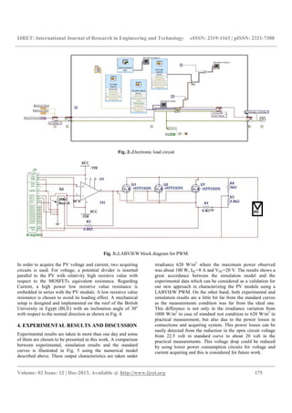
modulation (PWM) process is used to control the gate voltage
as illustrated in Fig. 3. The PWM frequency is set to 1 KHz
and a saw-tooth signal is used to vary the pulse duration. The
modulation process is developed by connecting the saw-tooth
generator with the duty cycle adjuster of the square wave
generator. The saw-tooth frequency is adjusted to be 1 Hz so
that a complete characterization process occurs in 1 sec with
1000 samples. In order to isolate the DAQ to avoid any
loading problem, a buffer is implemented using LM741 with
an adjustable gain to calibrate the operating point according to
the required gate voltage.](https://image.slidesharecdn.com/noveltechniqueincharactarizingapvmoduleusing-140807014257-phpapp01/85/Novel-technique-in-charactarizing-a-pv-module-using-2-320.jpg)
![IJRET: International Journal of Research in Engineering and Technology eISSN: 2319-1163 | pISSN: 2321-7308
__________________________________________________________________________________________
Volume: 02 Issue: 12 | Dec-2013, Available @ http://www.ijret.org 176
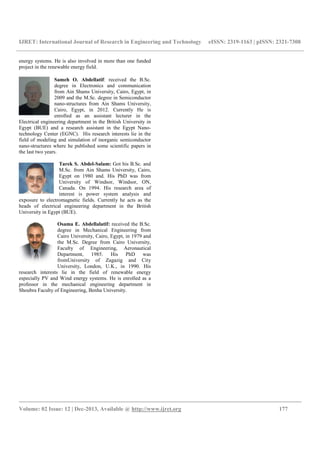
Fig. 4: Experimental setup for a 150 watt PV module.
Fig.5: I-V and P-V curves for a 150 Watt PV module (a)
under standard test conditions (b) Simulation results and (c)
experimental results.
CONCLUSIONS
The work in this paper presents a new approach in
characterizing a 150 Watt PV module using electronic load
circuit driven by pulse width modulator. Experimental results
are taken and compared with a precise developed simulator
based on Comsol Multiphysics. The experimental results
shows high accordance with simulation results. The suggested
systems shows a very high accuracy compared with the
previous published techniques with lower cost and complicity.
ACKNOWLEDGEMENTS
This work is funded by the British University in Egypt (BUE).
The authors acknowledge the valuable support of Prof. Hani
Ghali, the vice-dean of the faculty of Engineering, throughout
the work.
REFERENCES
[1]. VanDyk E.E., Gxasheka A. R., Meyer E.L. Monitoring
Current–Voltage Characteristics and Energy Output of Silicon
Photovoltaic Modules. ELSEVIER, Renewable Energy 30,
2005. p. 399–411,
[2]. Kuai Y., YuvarajanS.,An Electronic Load for Testing
Photovoltaic Panels. ELSEVIER, Journal of Power Sources
154, 2006. P.308–313.
[3]. Atia Y., Zahran M., Al-Hossain A. Solar Cell Emulator
and Solar Cell Characteristics Measurements in Dark and
Illuminated Conditions. Wseas Transactions On Systems And
Control, Issue 4, Volume 6, ISSN: 1991-8763. April 2011.
[4]. A. Sahbal, N.Hassan, M. Abdelhameed, A. Zekry,
Experimental Performance Characterization of Photovoltaic
Modules Using DAQ, TerraGreen 13 International Conference
2013 - Advancements in Renewable Energy and Clean
Environment, Energy Procedia 36 (2013) 323 – 332
[5]. Leite V., Chenlo F.An Improved Electronic Circuit for
Tracing the I-V Characteristics of Photovoltaic Modules and
Strings. In Proc. of the International Conference on
Renewable Energies and Power Quality (ICREPQ'10), March
23-25, 2010.
[6]. Leite V., Batista J., Chenlo F., Afonso J. Low-Cost
Instrument for Tracing Current-Voltage Characteristics of
Photovoltaic Modules. in Proc. of the International Conference
on Renewable Energies and Power Quality (ICREPQ'12),
March 28-30, 2012.
[7]. Comsol, Version 4.2, http://www.comsol.com.
[8]. Reference solar spectral irradiance: Air mass 1.5, National
Renewable Energy Lab.
http://rredc.nrel.gov/solar/spectra/am1.5/. Accessed 29
March2011.
[9]. Abdellatif, S., Kirah, K. ’’Nanowire photovoltaic
efficiency enhancement using plasmonic coupled nano-fractal
antennas ’ Optics Letters, Vol. 38, Issue 18, pp. 3680-3683,
2013.
[10]. Abdellatif, S, Kirah, K., Ghalli, H, .and Anis, W.’’
Spectral and Spatial Distributed Nanowire Array Enhanced by
Nanoring Optical Antenna ’’ Optical Materials Express, Vol. 2
Issue 10, pp.1432-1436 (2012)
[11]. ISTARSOLAR, http://www.istarsolar.com.
[12]. Hambley A. R. Electronics. 2nd edition. Prentice Hall.
Upper Saddle River. New Jersey 07458. 2000.
BIOGRAPHIES
IbrahemM. Mahmoud: received the B.Sc.
degree in Electrical Power and Machines
from Helwan University, Cairo, Egypt, in
2008 and a M.Sc. Student in Renewable
Energy at British University in Egypt, Cairo,
Egypt, Currently. Currently He is enrolled as
a demonstrator in the Electrical engineering department in the
British University in Egypt (BUE). His research interests lie
in the field of renewable energy especially PV and Wind
0 5 10 15 20 25
0
5
10
PV Voltage (volt)
PVCurrent(A)
0 5 10 15 20 25
0
100
200
PV Voltage (volt)
PVPower(Watt)
Simulation Results
Experimental Measurements
Standard Curve](https://image.slidesharecdn.com/noveltechniqueincharactarizingapvmoduleusing-140807014257-phpapp01/85/Novel-technique-in-charactarizing-a-pv-module-using-4-320.jpg)

This paper presents a novel technique for characterizing photovoltaic (PV) modules using an electronic load circuit driven by pulse width modulation (PWM) through LabVIEW. The proposed method achieves high accuracy and lower complexity compared to previous techniques, validated by experimental results matching simulation outputs from COMSOL Multiphysics and MATLAB. The approach addresses the limitations of standard testing conditions, providing a practical solution for real-world performance assessment of PV modules.