Downloaded 224 times


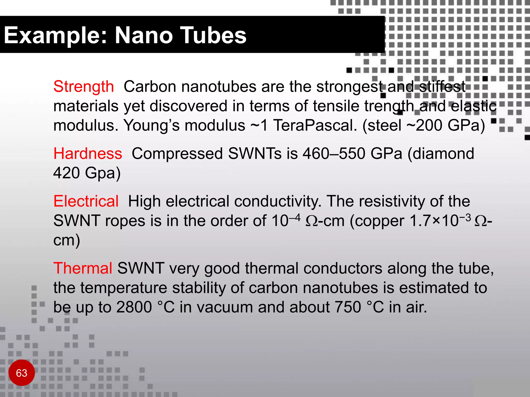
![Environment: Nano Solar Cells
Nano solar cells mixed in plastic could be
painted on buses, roofs, clothing
– Solar becomes a cheap energy alternative!
Source: http://www.berkeley.edu/news/media/releases/2002/03/28_solar.html
Nano solar cell: Inorganic nanorods embedded in semiconducting
polymer, sandwiched between two electrodes
] 200 nm
69](https://image.slidesharecdn.com/nanotechnologyintroduction-161003184634/75/Nanotechnology-introduction-69-2048.jpg)

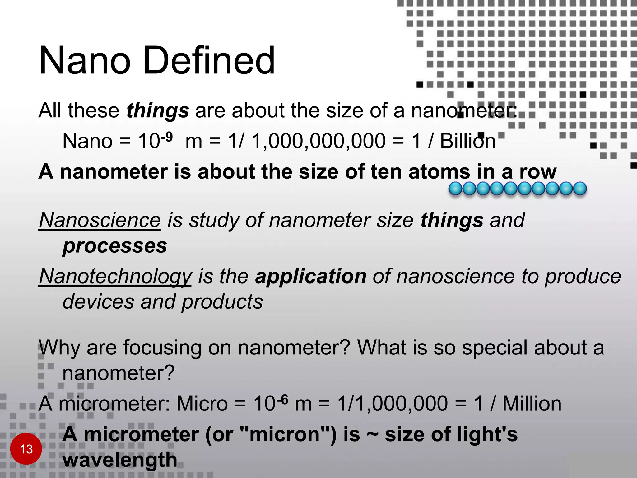
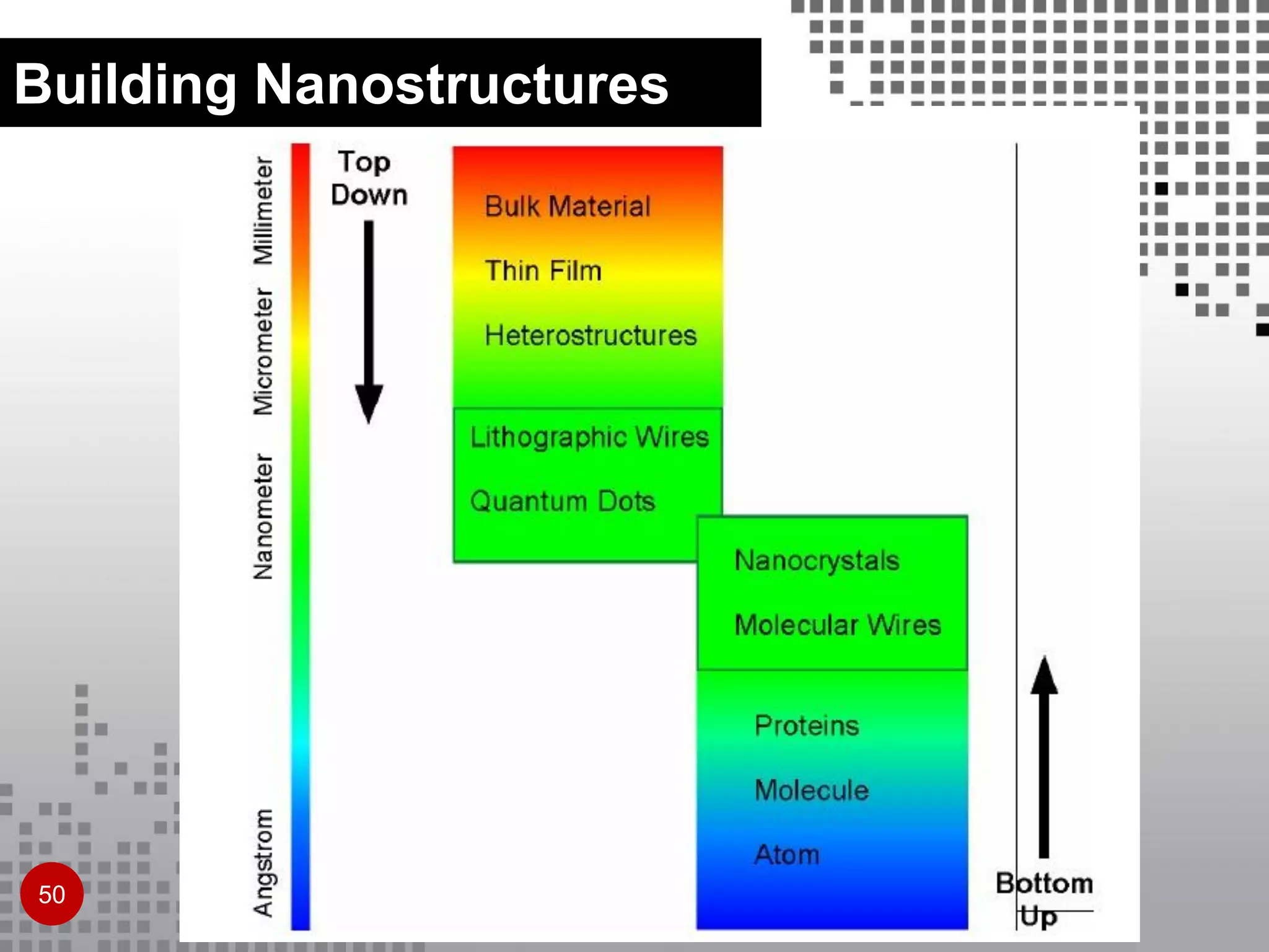
This document provides an introduction to nanotechnology. It begins with definitions of nanoscience and nanotechnology as the study and application of structures and processes at the nanometer scale, around 1 to 100 nanometers. Next, it discusses the tools that enabled nanoscience like the scanning electron microscope and scanning tunneling microscope which allow observation and manipulation of structures at the nanoscale. The document then outlines various nanostructures that exist in nature like biological machines and viruses, as well as man-made nanostructures like carbon nanotubes and buckyballs. It concludes with an overview of methods for building nanostructures including atom-by-atom assembly using scanning probe microscopes, sculpting materials away, and designing for self assembly.


