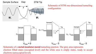
1. Schematic of STM one-dimensional tunneling
configuration.
Schematic of a metal-insulator-metal tunneling junction. The grey area represents
electron filled states (occupied level) and the white area is empty states, ready to accept
electrons (unoccupied level).
2. Schematic of a metal-insulator-semiconductor tunneling junction
3. An actual I-V curve of a
HOPG sample
Scanning tunneling spectroscopy (STS): extension of scanning tunneling microscopy (STM):
provides information on the density of electrons in a sample as a function of their energy.
The electron density is a function of both position and energy: described as the local density of electron states,
abbreviated as local density of states (LDOS), which is a function of energy.
Scanning tunneling spectroscopy (STS): measures the number of electrons (the LDOS) as a function of electron
energy. The electron energy is set by the electrical potential difference (voltage) between the sample and the
tip. The location is set by the position of the tip.
4. corresponding normalized differential tunneling
conductance. Metal – Insulator- Semiconductor
junction
the slope of the I-V curve at each voltage:
dI/dV-curve. :
more fundamental because dI/dV
corresponds to the electron density of
states at the local position of the tip, the
LDOS.
While STS can provide spectroscopic information with amazing spatial resolution, limitations
exist for chemical sensitivity since Tip-Sample bias range is limited to barrier height (𝜙)
STM and STS both deal with sample valence electron states. Element-specific information is
impossible since the chemical bond formation greatly perturbs the valence states.
5. the slope of the I-V curve at each voltage (dI/dV - curve) : dI/dV corresponds to the electron
density of states at the local position of the tip, the LDOS.
Differential conductance ((dI/dV)/(I/V) = d(ln(I))/d(ln(V)) as a function of voltage.
un
un
un
un
6. Interpretation of HOPG’s three-fold-hexagon pattern of STM images
(2.46 A0)
(1.4 nm x 1.4 nm)
1.42 A0