VIP Kolkata Call Girl Howrah 👉 8250192130 Available With Room
1 c -users_haider_app_data_local_temp_npse36c
1. Schottky diode operation
1 Ideal junction characteristics
The shottky-barrier diode is formed by a metal contact (anode) to a semiconductor
(the cathode), instead of the more common junction between P- and N-type
semiconductors. Shottky diodes differ from PN-junction devices in that rectification
occurs because of differ in work function between the metal contact and the
semiconductor, rather a nonuniform doping profile. Conduction is not controlled by
minority carrier recombination in the semiconductor, but by thermionic emission of
majority carriers over the barrier created by the unequal work functions. The Schottky
diode is, therefore, a majority carrier device whose switching speed is not limited by
minority carrier effects.
Many metals can create a Shottky barrier on either silicon or GaAs
semiconductors. For GaAs the most common are platinum, titanium and gold.
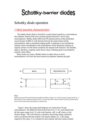
Fig.1
Band structure of the metal and semiconductor before contact. E0 is the free-space energy level, EC is
the bottom of the conduction band, and Ev is on the top of the valence band. Efm and Efs are the Fermi
levels in the metal and semiconductor, respectively.
Figure 1 shows the energy band diagrams of a metal and an N-type
semiconductors. The difference between the Fermi level Ef for each material and
the free-space energy level E0 is the work function , qφm or qφs ,where q is the
electron charge . The work function is, therefore, the average energy required to
remove an electron from the material .The electron affinity, qX , is the energy
required to free space. X is a constant for each material, and must remain constant
2. throughout it. However, the Fermi level of the semiconductor, and hence its work
function, can be expected to vary with doping density.
When the metal and semiconductor are in equilibrium and are not in contact, the
energy levels are constant throughout the materials .The Fermi levels are generally
unequal, indicating that the electrons in one material (in this case the metal) have less
energy, on the average, than these in the semiconductor. Therefore, when the
materials are joined, some of the electrons in the semiconductor move spontaneously
into the metal and collect on the surface. These leave behind ionized donor locations,
which are positively charged, and create a negative surface charge where they collect
on the surface of the metal. An electric field is set up between these positive charges
and the electrons that eventually inhibits further electron flow into the metal. The
positively charged region is called a depletion region, since it is almost completely
depleted of mobile electrons.
The shape of the energy diagram of the metal-semiconductor junction is governed
by three rules:
1. In equilibrium, the Fermi levels for the semiconductor and metal must be constant
throughout the system;
2. The electron affinity must be constant;
3. The free-space energy level must be continuous.
Fig.2
(a)Band structure of the Shottky junction; (b) charge densities at the junction (the negative component
is the surface electron concentration on the metal); (c) electric field in the depletion region.
Figure 2a shows the resulting band structure when the metal and semiconductor
are joined. In order to satisfy all three rules simultaneously, the valence and
3. conduction bands of the semiconductor are forced to bend at the junction; the upward
bend of the conduction band of the N-type semiconductor indicates depletion region.
The resulting potential difference across this region, as shown in the figure, is simply
the difference between the work function, φbi = φm - φs. This is called the built-in
potential of the junction.
The positively charge depletion region in the semiconductor, can be considered to
be an area of stored charge. Indeed charge has been moved onto the metal contact,
one "plate " of the capacitor, and off the semiconductor, the other "plate ", by the
application of the built-in potential difference. Before it is possible to determine the
capacitance, it is necessary to find the quality of charge that has been moved, which is
equal to the depletion zone charge. The depletion zone charge density to known:
because the depletion zone charge is due to donor atoms, all of which are ionized, it is
equal to the doping density. The junction area is, of course, known, but the width of
depletion zone still must be found be found in order to determine the total charge.
The electric field in the depletion zone is found by applying the Gauss law to the
region. It should be obvious that the electric field is in the negative x direction (fig2),
and that it is maximum at the junction. It must also be zero at the edge of the
depletion region, because E=-dφ/dx=0, as evidenced by the flat band at this point.
Secondly, the voltage across the junction, found by integrating the electric field, must
equal φbi. Applying the Gauss law in one dimension,
(1) dE(x) / dx = ρ(x) / εs = qNd / εs
(2) E(x) = Emax(1-x/d)
where
(3) F=-qNdd/εs
Emax - maximum electric field
d- depletion width
Nd- doping density (assumed uniform)
εs -dielectric permittivity of the semiconductor
εs -=13.1∗ ε0 for GaAs
εs -=11.9∗ ε0 for silicon
ε0 =8.854∗ 10 F cm-1
-14
An assumption used in deriving (1) to (3) is that the edge of the depletion region is
abrupt; i.e., there is no gradual variation in charge density between the depletion
region and undepleted semiconductor. This assumption is called the depletion
approximation. In fact, a narrow transition region does exist, but it effect is negligible
for most purposes.
Since E (x) is a simple triangle function, it is easily integrated to give
(4) φbi = Emax d/2 = qd2 Nd / 2εs
The resulting depletion width d, is
(5) d= 2 φbi εs / q Nd
4. The charge contained in the depletion region is found from the donor density and the
dimensions of the region, which are known. The depletion charge, QJ , is
(6) QJ = qWd Nd = W 2q φbi es Nd
where W is the area of junction. This relates directly to the junction capacitance.
2 Ideal I/V characteristic and junction capacitance
Fig.3
Fig.3 biased Schottky junction: (a) forward bias; (b) reverse bias. The Fermi levels are offset by an
amount to the applied voltage.
Figure 3 shows a biased Schottky junction. Since biased is applied, the junction
is no longer in equilibrium, and the requirement that the Fermi levels be constant
throughout the diode no longer applies. Instead, the Fermi levels (which should
rightly be called quasi-Fermi levels for the nonequilibrium case), move with applied
voltage. The offset from their equilibrium position is simply equal to qV, where V is
the applied voltage. The voltage across the junction then is φbi -V, where V is defined
as positive with polarity that forward-biased the junction. The expression for electric
field E (x), maximum electric field Emax , depletion region d, and charge QJ are still
valid for the biased diode as long as the potential φbi -V. the resulting expressions for
charge and depletion width are as follows:
(7) QJ = W 2q es Nd(φbi -V)
(8) d= 2 es (φbi -V) / q Nd
5. The capacitance of charge with junction voltage. Taking this derivative, the junction
capacitance is found:
(9) d QJ /dV = C(V) = W q es Nd /2(φbi -V) = Wes/d
This can be put into the form
(10) C(V) = CJ0/(1-Vφbi)1/2
which is most useful for circuit analysis. CJ0 is the junction capacitance at zero bias
voltage.
The exponent 1/2 in the denominator of (10) comes from the assumption that the
doping density Nd is constant throughout the semiconductor. In practice, Nd may not
be uniform, thus changing the exponent .One of the most dramatic examples of this is
the Mott diode, the capacitance of which has relatively weak dependence on voltage.
The junction can be found by several methods, which give the same general
voltage dependence. The following derivation is simple and intuitively satisfying.
Electron conduction occurs primarily by thermionic emission over the barrier.
This emission occurs equally in the both directions in equilibrium, at zero bias, giving
no net current. When forward bias is applied, electron energy is increased relative to
the barrier height, allowing increased electron emission from the semiconductor into
the metal. The current component in the opposite direction stays constant.
The electron density at junction, n1 , can be found from the Maxwell-Boltzmann
distribution. It is given by
(11) n1 = Nd exp(-qφbi /KT)
under zero bias conditions. The current in each direction is equal, and must be
proportional to this electron density. Under bias, the potential barrier becomes φbi-V,
and therefore the density of forward-conducted electrons is
(12) n2 = Nd exp[-q(φbi-V )/KT]
where K is Boltzmann's constant (1.37∗ 10-23 J/K) and T is absolute temperature. The
current is proportional to the difference between these densities,
(13) I(V)= I0 [exp(qV/KT) -1]
Equation (13) is called the ideal diode equation. In order to compensate for nonideal
behavior, it is usually modified to form
(14) I(V)= I0 [exp(qV/nKT) -1]
Where n is a number close to 1.0, usually between 1.05 and 1.25, called the slope
parameter or ideality factor.
Calculation of the current parameter I0 is much more complicated task, and probably
futile , since I0 can be dominated by second-order effects such as leakage charge
generation , and tunneling. Nevertheless, an ideal expression for I0 can be found by
assuming that all current conduction is by thermionic emission. It is given by
6. (15) I0 = A ** T2 Wexp(-qφbi /KT)
where A ** is the modified Richardson constant, W is the junction area, and φbi is the
barrier height (difference between the Fermi level and the peak of the conduction
band). A ** is approximately 96 A cm-2 K -2 for silicon 4.4 A cm-2 K -2 for GaAs. The
low value of thee Richardson constant for GaAs implies that the knee of the I/V
characteristic occurs at higher applied voltages for GaAs diodes.
3 Deviations from the Ideal Case
Real Schottky diodes do not always follow the expressions derived before.
Deviations from ideal behavior arise from imperfections in fabrication or factors,
which are not included in this relatively simple theory. A few of the major limitations
are given below.
1.Schottky Barrier Lowering
It was assumed that the Schottky barrier height remained constant under all
conditions of applied voltage. In fact, the barrier height varies with applied voltage
because conduction electrons experience a force from their image charges in the
metal. This force attracts the electrons toward the metal surface, effectively lowering
the barrier, and allowing voltage-dependent deviations from ideal behavior. In theory,
this "image force" should give the reverse current a fourth-power dependence of bias
upon voltage, rather than the constant value implied by (14).
This effect is usually not observed, because carrier generation in the depletion
region at high reverse bias and tunneling effects dominate reverse leakage.
At forward biases above approximately 0.1 V, the effect is to cause the
ideality factor n to deviate slightly from unity. For a diode that is ideal expect for
barrier lowering, the ideality factor is
(16) n = 1/(1-dφbi /dV)
where dφbi /dV is the variation in barrier height with applied voltage. The relation for
this quantity is.
(17)
dφb 1 q 3 Nd φbi - V- φfc - KT -3/4
dV 4 8π2 εs3 q
where φfc is the potential difference between the Fermi level and bottom of the
conduction band. As for the reverse case, this quantity rarely dominates the ideality
factor; for Nd = 1017 cm-3 , n is only 1.02.
2. Surface Imperfections
7. The semiconductor surface must be extremely clean in order to realize I/V
characteristics approximately the ideal. However, in spite of scrupulous care in
fabrication, the junction experiences at least a small amount of contamination due to
impurities. The deposition of the junction metal may also damage the crystal structure
of the surface, especially if sputtering techniques are used. Formation of undesired
chemical compounds between the junction metal and the semiconductors may also
occur, especially if the diode is subjected to high temperatures. Although diodes are
rarely exposed to high temperatures in use, they are frequently exposed to high
temperatures as part of the fabrication process, such as annealing to repair sputtering
damage, attaching to a circuit, or as innocent bystanders when other components
soldered into the mixer. The effect is to increase both the ideality factor and, in some
cases, reverse conduction. Surface imperfections are probably the major cause of
nonideal behavior in Schottky diodes.
3.Tunneling
Thermal emission is not only mechanism by which electrons can cross the
potential barrier at the junction. Quantum mechanical tunneling through the barrier is
also possible, and may have a significant effect on I/V characteristic at low
temperatures and high doping densities. Tunneling is often responsible for "soft" I/V
characteristics (i.e., high n) at low currents. It is of particular significance in devices
designed for cryogenic operation because, as temperatures are lowered, the current
component due to tunneling does not decrease as rapidly as the thermionic
component. Tunneling also increases the noise temperature of the diode.
4.Series Resistance
Schottky junctions generally require lightly doped semiconductors with
relatively high bulk resistivities. A lightly doped substrate would not be practical for
diode fabrication because it would result in high series resistance and poor ohmic
cathode contacts. Practical diodes are, therefore fabricated on a lightly doped, thin
epitaxial layer that is grown on a heavily doped, low resistance substrate. This
structure allows the lightly doped region to be used for the junction and the heavily
doped region to minimize series resistance. A high-quality ohmic contact can be made
to this heavily doped substrate.
The undepleted epitaxial layer may still contribute to series resistance (Rs)
because the epitaxial layer must be made thick enough to contain the depletion region,
even at high reverse bias. For example, for a diode with an epitaxial doping density of
2X10¹⁷ , the depletion depth at zero applied voltage is approximately 750 angstroms.
This requires an epitaxial thickness of 1000-2000 angstroms to contain the depletion
layer at 5-6 V reverse bias. At forward bias, however, there may be 500-1500
angstroms of undepleted, high-resistance expitaxial material under the junction.
The remaining bulk resistance of the substrate and its ohmic contact, as well as the
undepleted epitaxial area, may leave several ohms of resistance in series with the
junction. The resistance creates power losses, which are often substantial, especially
in millimeter-wave mixers, where the junction area is very small. Series resistance
often creates a lower limit to the diode size, which can be used; sub-micron diameter
diodes can be fabricated with present technology, but series resistance usually limits
practical sizes to 1.5-2.0µm.
8. It is difficult to describe a general procedure for estimating series resistance,
because it is strongly dependent on diode structure. Estimation is further complicated
by the fact that the skin effect causes the diode current to exist in the surface of the
substrate, rather than in its bulk, at frequencies, above approximately 50 GHz.
Similarly, at high frequencies, the whisker or other connecting wire may have several
ohms of series resistance due to the skin effect.
For example, the series resistance of a dot-matrix diode at high frequencies is
estimated by first determining the current path in the chip. The current path is shown
in figure (4). The current flows from the anode through the expitaxial layer, and
spreads out because of the skin effect along the top surface of the chip to its edge.
Because the substrate resistivity is much lower then that of the epitaxial layer, the
current exists primarily in the substrate. It then flows down the sides of the chip to the
mounting surface.
Fig.4
Current distribution in the dot-matrix diode.
Therefore, the series resistance consists of three components: the undepleted
epitaxial layer under the junction, the spreading resistance of the top side of the diode
between the anode and the sides of the chip, and the resistance of the edges. Because
it is thin compared to the diode diameter, there is little current spreading in the
epitaxial layer. The resistance of the epitaxial layer is that of a cylinder of material:
(18) R d1 = (t - d)/qNd µa 2
where t is the epitaxial layer thickness, d is the depletion width, and µ is the electron
mobility. The spreading resistance component is found by first approximating the chip
as a cylinder with the anode in the center, and is approximately
(19) R d2 = ln(b/a)/2πδqNd µ
where a is the anode diameter, b is the diameter of the chip ( which can be
approximated as a side length for the more common square chip ), and δ is the skin
depth in the substrate material. The sidewall resistance is given by
9. (20) R d3 = h/4πbδqNd
where h is the chip height and w is the side width. This estimate for R d3 may be low
because mechanical damage or roughness of the side of the chip increases R d3 .
The high-frequency series resistance is the sum of the three components:
( 21) R s = R d1 + R d2 + R d3
Of course, the series resistance measured at do includes only R d1 ; without skin effect,
R d2 and R d3 are the bulk do resistance of the substrate, which is negligible compared
to R d1 . Diode series resistance specified by manufacturers invariably the do value.
5.Edge Effects
The expressions in section 2 all assume that the electric field is perpendicular to
the junction over its entire area. However, practical diodes are formed with a small
anode on a large semiconductor surface, so the fringing electric field near the edge of
the metal anode is greater then that in the center. The current density is, therefore,
greatest at the edge of the junction, and may be relatively low at the center. As a
periphery than its area. For this reason, small diodes are sometimes fabricated with
metal geometries, such as a cross shape, which increase the periphery to reduce series
resistance, and to reduce the area in order to minimize capacitance.