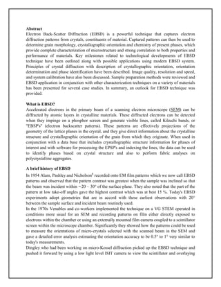
SlideShare a Scribd company logo
1 of 9
Download to read offline
Assignment No.1
Electron Backscatter Diffraction (EBSD)
Subject: Material Science
Assigned date: Dec. 20, 2015
Submission date: Jan. 10, 2016
Submitted to: Dr. Salamat Ali
Submitted by: Imtiaz Ali
Abstract
Electron Back-Scatter Diffraction (EBSD) is a powerful technique that captures electron
diffraction patterns from crystals, constituents of material. Captured patterns can then be used to
determine grain morphology, crystallographic orientation and chemistry of present phases, which
provide complete characterization of microstructure and strong correlation to both properties and
performance of materials. Key milestones related to technological developments of EBSD
technique have been outlined along with possible applications using modern EBSD system.
Principles of crystal diffraction with description of crystallographic orientation, orientation
determination and phase identification have been described. Image quality, resolution and speed,
and system calibration have also been discussed. Sample preparation methods were reviewed and
EBSD application in conjunction with other characterization techniques on a variety of materials
has been presented for several case studies. In summary, an outlook for EBSD technique was
provided.
What is EBSD?
Accelerated electrons in the primary beam of a scanning electron microscope (SEM) can be
diffracted by atomic layers in crystalline materials. These diffracted electrons can be detected
when they impinge on a phosphor screen and generate visible lines, called Kikuchi bands, or
"EBSP's" (electron backscatter patterns). These patterns are effectively projections of the
geometry of the lattice planes in the crystal, and they give direct information about the crystalline
structure and crystallographic orientation of the grain from which they originate. When used in
conjunction with a data base that includes crystallographic structure information for phases of
interest and with software for processing the EPSP's and indexing the lines, the data can be used
to identify phases based on crystal structure and also to perform fabric analyses on
polycrystalline aggregates.
A brief history of EBSD
In 1954 Alam, Pashley and Nicholson6
recorded onto EM film patterns which we now call EBSD
patterns and observed that the pattern contrast was greatest when the sample was inclined so that
the beam was incident within ∼20 – 30° of the surface plane. They also noted that the part of the
pattern at low take-off angles gave the highest contrast which was at best 15 %. Today's EBSD
experiments adopt geometries that are in accord with these earliest observations with 20°
between the sample surface and incident beam routinely used.
In the 1970s Venables and co-workers implemented the technique on a VG STEM operated in
conditions more usual for an SEM and recording patterns on film either directly exposed to
electrons within the chamber or using an externally mounted film camera coupled to a scintillator
screen within the microscope chamber. Significantly they showed how the patterns could be used
to measure the orientations of micro-crystals selected with the scanned beam in the SEM and
gave a detailed error analysis estimating the orientation accuracy to be 0.5° to 1° very similar to
today's measurements.
Dingley who had been working on micro-Kossel diffraction picked up the EBSD technique and
pushed it forward by using a low light level ISIT camera to view the scintillator and overlaying
the video output from this with graphics from a BBC micro-computer allowing a significant
increase in the rate of pattern indexing and orientation measurements. This is one of the very
earliest attempts at integrating capture of video information at a microscope to enable
quantitative on-line analysis. Pattern indexing methods were improved so that minimal user input
of only 3 zone axes positions were required to index and calculate orientations for patterns from
cubic crystals, non-cubic crystals and full automation of the analysis set as a clear goal very early
on. The main materials science challenge EBSD was aimed at in these early days was in grain
boundary characterization, a theme that continues to this day, and in particular identifying any
significant special properties associated with low CSL boundaries, e.g. other topics that were
explored were possibilities for phase identification including combining EBSD with local
chemistry from EDX. A further notable study by Baba-Kishi and Dingley attempted to
distinguish between different space and point groups from symmetry elements and systematic
reflections in EBSD, again a topic that has been returned to more recently with much greater
image analysis and computing power available now.
The next big advance in the method came with automation of the band detection step which
finally allowed the whole process of pattern collection and indexing to be undertaken without
user intervention. By adding in computer control of the SEM beam position it was then a
relatively simple task to implement EBSD orientation mapping. The Yale group of Adams,
Wright, and Dingley (on sabbatical from Bristol) first implemented a Burns algorithm for band
detection but moved to the modified Hough transform which the Risø group (Krieger Lassen,
Juul Jensen and Conradsen) had shown to be successful. Both groups had successfully
implemented automated EBSD mapping by the early 1990s.
Goehner and Micheal showed that phase discrimination is possible by comparing measured
interplanar angles to those expected from the known crystallography for each of a wide range of
possible phases held in a database. The problem to be overcome here is in reducing the number
of possible phases to a manageable level either through knowledge of local chemistry or by the
primitive lattice volume.
FIGURE 2.1. Seishi Kikuchi (standing). Thanks to Professor Shun Karato, Yale University,
Geology Department. Originally published in Scientific American. Photo credit Nishina
Memorial Foundation, courtesy of Hiroshi Ezawa.
FIGURE 2.2. Kikuchi P-pattern from calcite cleavage.
FIGURE 2.3. Kikuchi P-pattern from mica.
FIGURE 2.4. Boersch 1937 Iron Kikuchi patterns.
How does EBSD work?
The polished sample is placed in the SEM and inclined approximately 70o
relative to normal
incidence of the electron beam. The detector is actually a camera equipped with a phosphor
screen integrated with a digital frame grabber. The camera resides on a horizontally mounted
motorized carriage. It is inserted to within several mm of the surface of the inclined sample. The
optimal arrangement results when the camera is as close to the sample as possible while avoiding
the possibility of collision between the sample surface and the delicate phosphor screen. The
pattern of Kikuchi lines on the phosphor screen is electronically digitized and processed to
recognize the individual Kikuchi lines. These data are used to identify the phase, to index the
pattern, and to determine the orientation of the crystal from which the pattern was generated.
[Insert ebsp_index.jpg here - improve this later with a picture of a crystal showing orientation
below the indexed pattern] Individual mineral grains can be selected for identification and
determination of crystal orientation, or data may be acquired on a grid over a selected area of the
surface of the sample to determine the identity, orientations, and spatial relations between a large
number of grains.
These data can be used to make statistical studies of the micro-fabric of the sample, to reveal
systematic textural relations between individual grains or phases, and even to determine relative
abundances of phases in a poly-phase sample.
Application areas
EBSD has now been used for many aspects of materials characterization including
characterization of grain boundary types, establishing epitaxial relationships between layers on
substrates in metal, semiconductor and superconductor systems, characterizing texture and its
changes during deformation and annealing in metal alloys and geological samples, establishing
links between grain size and texture components during deformation and annealing, contributing
to determination of grain boundary energy through thermal grooving, and ex situ and in
situ experiments on grain boundary mobility.
Over the last two decades an ample of research has been conducted using EBSD technique on
various materials, initially carried at universities and research centers and lately in industry as
well. Today, besides continuous increase in research activity by employing EBSD worldwide,
the technique is also finding its way to complement other techniques and contributes to more
detailed microstructure characterization and better understanding of material properties. Several
such examples are presented below.
 EBSD and nano-indentation
 EBSD and energy dispersive spectroscopy
 EBSD and atomic force microscopy
Strengths
EBSD is unquestionably the fastest and most reliable way in which to acquire data for crystalline
structure and orientation in a solid crystalline phase. Unlike optical techniques, it is possible to
acquire data for phases of all symmetries (even isotropic phases) and for opaque phases. The data
give true 3-dimensional orientations for individual crystals, which is superior to optical pole
figures which give 2-dimensional orientations. The spatial resolution can be on the order of
several microns, which is much superior to resolution attainable using selected area channeling
(SAC) techniques. EBSD data acquired using either a scanned electron beam, or (better) an
automated stage and a stationary electron beam can include analyses of thousands of individual
grains in a run accomplished in hours; acquisition of data for 10's of thousands of individual
spots in a single one-day run is routine in most laboratories. TEM can yield excellent diffraction
data with exceptionally high spatial resolution for individual crystals, but sample preparation is
considerably more involved than it is for EBSD studies, and most TEM mounts can only be
examined over an area that is relatively small compared with areas accessible using EBSD.
Limitations
 Specialized Sample Preparation Requirements: EBSP's are generated at very
shallow depths within the sample, so appropriate samples must be free of damage
to the crystal lattices at the surface of the sample. Mechanical grinding and
polishing in routine preparation of polished samples (such as microprobe samples)
results in significant damage to crystal lattices near the surface of most materials.
Therefore, it is necessary to perform additional chemical polishing on samples
after they have been polished using abrasives. This is a labor-intensive and time-
consuming process that requires experience with the materials of interest for
optimal results.
 Problems with Application of Conductive Coatings: Since EBSP's are generated
very near the surface of the sample, the application of a conductive coating to
electrically insulating materials is highly undesirable. SEMs capable of operation
in a low-vacuum mode can be used to examine electrically insulating materials
without application of a conductive coating and this capability is highly desirable
in EBSD work on many materials, including oxides and silicates of interest in most
geological applications.
 Data are best acquired with a stationary beam, or with the beam scanning over a
small area of the sample (high magnification). At lower magnifications, the angle
of incidence of the beam on the periphery of the area of interest creates artifacts in
the EBSP and the data become difficult to index accurately. The best solution is to
use a stationary beam (scanning mode off) and acquire data over the area of
interest by moving the sample. The procedure requires an automated specimen
stage, and data acquisition is considerably slower than acquisition using beam
scanning.
Conclusions
The use of the EBSD detector as an imaging device allows for a great amount of flexibility in
image formation. Through extreme binning of the EBSD CCD camera it is possible to collect
images at a rate comparable to slow scan imaging in the SEM. VFSD data can also be collected
concurrently with the usual orientation data during an EBSD scan. If patterns are recorded,
VFSD images can be formed with even more flexibility during post-processing.
By forming composite images of the simultaneously collected images it is possible to suppress or
isolate the contrast of interest. Determining the best recipe for highlighting a particular micro-
structural feature is not always obvious and changes with different samples, SEM/EBSD
geometry and SEM/EBSD operating conditions. Nonetheless, having the flexibility of utilizing
VFSD images provides a myriad of combinations for characterizing different aspects of
microstructure.
It should be emphasized that the EBSD patterns need not be of sufficient quality for indexing.
Images can be formed from surfaces too rough to produce index-able patterns. Thus, like SEI
and BEI, the VFSD images provide only visualizations of the microstructure—they do not
contain the quantitative data intrinsic to conventional OIM maps. However, VFSD images can be
combined with conventional EBSD and XEDS mapping and correlative imaging between all of
these techniques can be realized.
It is beyond the scope of this work to explore in detail all of the aspects of this imaging
technique. We have begun investigating the potential of using VFSD in phase differentiation,
automated directed scanning, and measuring crystallographic texture; however, these new areas
are just being explored and we expect other application areas, more detailed analysis of the
physical phenomena and more quantitative data processing approaches to emerge.
References
1. S. Kikuchi, ―Diffraction of cathode rays by mica‖,
Jpn. J. Phys., 5 (1928) 83–96.
2. S.I. Wright, Ph.D. Thesis, Yale University, USA
1992.
3. S. Nishikawa, S. Kikuchi, ―The diffraction of cathode
rays by calcite‖, Proc. Imperial Acad. Jpn., 4 (1928)
475–477.
4. R. von Meibom, E. Rupp, ―Wide angle electron diffraction‖,
Z. Physik, 82 (1933) 690–696.
5. H. Boersch, ―About bands in electron diffraction‖,
Physikalische Zeitschrift, 38 (1937) 1000–1004.
6. K. Artmann, ―On the theory of Kikuchi bands‖, Z.
Physik, 125 (1948) 225–249.
7. M.N. Alam, M. Blackman, D.W. Pashley, ―High-angle
Kikuchi patterns‖, Proc. Royal Society of London,
A221 (1954) 224–242.
8. J.A. Venables, C.J. Harland, ―Electron back-scattering
patterns – A new technique for obtaining crystallographic
information in the scanning electron microscope‖,
Philoso. Mag., 2 (1973) 1193–1200.

More Related Content

What's hot (20)

WDS
WDSWDS
WDS
 
Sintering
SinteringSintering
Sintering
 
Sintering
SinteringSintering
Sintering
 
Ti alloys
Ti alloysTi alloys
Ti alloys
 
Superalloys
SuperalloysSuperalloys
Superalloys
 
Characterization techniques
Characterization techniquesCharacterization techniques
Characterization techniques
 
01 fundamentals of metalworking
01 fundamentals of metalworking01 fundamentals of metalworking
01 fundamentals of metalworking
 
Super alloy
Super alloySuper alloy
Super alloy
 
Residual stress measurement techniques
Residual stress measurement techniquesResidual stress measurement techniques
Residual stress measurement techniques
 
Metallography and microscopy
Metallography and microscopyMetallography and microscopy
Metallography and microscopy
 
Thin film fabrication using thermal evaporation
Thin film fabrication using thermal evaporationThin film fabrication using thermal evaporation
Thin film fabrication using thermal evaporation
 
Metallurgical microscope / OPTICAL (METALLOGRAHY)
Metallurgical microscope / OPTICAL (METALLOGRAHY)Metallurgical microscope / OPTICAL (METALLOGRAHY)
Metallurgical microscope / OPTICAL (METALLOGRAHY)
 
Introduction to Mechanical Metallurgy (Our course project)
Introduction to Mechanical Metallurgy (Our course project)Introduction to Mechanical Metallurgy (Our course project)
Introduction to Mechanical Metallurgy (Our course project)
 
Sintering
SinteringSintering
Sintering
 
BULK METALLIC GLASS
BULK METALLIC GLASSBULK METALLIC GLASS
BULK METALLIC GLASS
 
INTERMETALLICS
INTERMETALLICSINTERMETALLICS
INTERMETALLICS
 
Dr.R.Narayanasamy - Super Plasticity
Dr.R.Narayanasamy - Super PlasticityDr.R.Narayanasamy - Super Plasticity
Dr.R.Narayanasamy - Super Plasticity
 
Metallography material engineering
Metallography material engineeringMetallography material engineering
Metallography material engineering
 
Mg alloys
Mg alloysMg alloys
Mg alloys
 
Micromolding - in depth insights
Micromolding - in depth insightsMicromolding - in depth insights
Micromolding - in depth insights
 

Similar to EBSD Technique Explained: Principles, Applications and Case Studies of Electron Backscatter Diffraction

Electron backscatter diffraction (EBSD).pptx
Electron backscatter diffraction (EBSD).pptxElectron backscatter diffraction (EBSD).pptx
Electron backscatter diffraction (EBSD).pptxKalpajyoti Mazumdar
 
3D EBSD Overview - Metallurgical Mater Trans A Vol 39 A (2008) 374
3D EBSD Overview - Metallurgical Mater Trans  A Vol 39 A (2008) 3743D EBSD Overview - Metallurgical Mater Trans  A Vol 39 A (2008) 374
3D EBSD Overview - Metallurgical Mater Trans A Vol 39 A (2008) 374Dierk Raabe
 
Probing electrical energy storage chemistry and physics over broad time and ...
Probing electrical energy storage chemistry and physics over broad time  and ...Probing electrical energy storage chemistry and physics over broad time  and ...
Probing electrical energy storage chemistry and physics over broad time and ...Andrew Gelston
 
120_SEM_Special_Topics.ppt
120_SEM_Special_Topics.ppt120_SEM_Special_Topics.ppt
120_SEM_Special_Topics.pptzaki194502
 
Electron Diffraction Using Transmission Electron Microscopy
Electron Diffraction Using Transmission Electron MicroscopyElectron Diffraction Using Transmission Electron Microscopy
Electron Diffraction Using Transmission Electron MicroscopyLe Scienze Web News
 
Biophys j savin05
Biophys j savin05Biophys j savin05
Biophys j savin05crazyduddy
 
PNAS-2013-Man-15886-91
PNAS-2013-Man-15886-91PNAS-2013-Man-15886-91
PNAS-2013-Man-15886-91Devin Liner
 
Matteo Correnti: Constraining Globular Clusters Properties Using IR Photometr...
Matteo Correnti: Constraining Globular Clusters Properties Using IR Photometr...Matteo Correnti: Constraining Globular Clusters Properties Using IR Photometr...
Matteo Correnti: Constraining Globular Clusters Properties Using IR Photometr...JeremyHeyl
 
THREE DIMENSIONAL ELECTRON MICROSCOPY AND IN SILICO
THREE DIMENSIONAL ELECTRON MICROSCOPY AND IN SILICOTHREE DIMENSIONAL ELECTRON MICROSCOPY AND IN SILICO
THREE DIMENSIONAL ELECTRON MICROSCOPY AND IN SILICOChetan Meena
 
Artificial periodic substrates
Artificial periodic substratesArtificial periodic substrates
Artificial periodic substratesRajeev Kumar
 
Zach & Matt PosterV2
Zach & Matt PosterV2Zach & Matt PosterV2
Zach & Matt PosterV2Zach Diener
 
Intro to Soft x ray vector ptycho tomography.pptx
Intro to Soft x ray vector ptycho tomography.pptxIntro to Soft x ray vector ptycho tomography.pptx
Intro to Soft x ray vector ptycho tomography.pptxstarbowtw
 
DOUBLE-TIP ARTEFACT REMOVAL FROM ATOMIC FORCE MICROSCOPY IMAGES
DOUBLE-TIP ARTEFACT REMOVAL FROM ATOMIC FORCE  MICROSCOPY IMAGESDOUBLE-TIP ARTEFACT REMOVAL FROM ATOMIC FORCE  MICROSCOPY IMAGES
DOUBLE-TIP ARTEFACT REMOVAL FROM ATOMIC FORCE MICROSCOPY IMAGESNexgen Technology
 
Methods of investigation of structure
Methods of investigation of structureMethods of investigation of structure
Methods of investigation of structureSCE.Surat
 
Fractal characterization of dynamic systems sectional images
Fractal characterization of dynamic systems sectional imagesFractal characterization of dynamic systems sectional images
Fractal characterization of dynamic systems sectional imagesAlexander Decker
 

Similar to EBSD Technique Explained: Principles, Applications and Case Studies of Electron Backscatter Diffraction (20)

Electron backscatter diffraction (EBSD).pptx
Electron backscatter diffraction (EBSD).pptxElectron backscatter diffraction (EBSD).pptx
Electron backscatter diffraction (EBSD).pptx
 
3D EBSD Overview - Metallurgical Mater Trans A Vol 39 A (2008) 374
3D EBSD Overview - Metallurgical Mater Trans  A Vol 39 A (2008) 3743D EBSD Overview - Metallurgical Mater Trans  A Vol 39 A (2008) 374
3D EBSD Overview - Metallurgical Mater Trans A Vol 39 A (2008) 374
 
Probing electrical energy storage chemistry and physics over broad time and ...
Probing electrical energy storage chemistry and physics over broad time  and ...Probing electrical energy storage chemistry and physics over broad time  and ...
Probing electrical energy storage chemistry and physics over broad time and ...
 
Connecting theory with experiment: A survey to understand the behaviour of mu...
Connecting theory with experiment: A survey to understand the behaviour of mu...Connecting theory with experiment: A survey to understand the behaviour of mu...
Connecting theory with experiment: A survey to understand the behaviour of mu...
 
2010_JAS_Database
2010_JAS_Database2010_JAS_Database
2010_JAS_Database
 
Fisica digital de Rocas
Fisica digital de RocasFisica digital de Rocas
Fisica digital de Rocas
 
120_SEM_Special_Topics.ppt
120_SEM_Special_Topics.ppt120_SEM_Special_Topics.ppt
120_SEM_Special_Topics.ppt
 
Electron Diffraction Using Transmission Electron Microscopy
Electron Diffraction Using Transmission Electron MicroscopyElectron Diffraction Using Transmission Electron Microscopy
Electron Diffraction Using Transmission Electron Microscopy
 
Biophys j savin05
Biophys j savin05Biophys j savin05
Biophys j savin05
 
POSTER_RONAK
POSTER_RONAKPOSTER_RONAK
POSTER_RONAK
 
PNAS-2013-Man-15886-91
PNAS-2013-Man-15886-91PNAS-2013-Man-15886-91
PNAS-2013-Man-15886-91
 
Matteo Correnti: Constraining Globular Clusters Properties Using IR Photometr...
Matteo Correnti: Constraining Globular Clusters Properties Using IR Photometr...Matteo Correnti: Constraining Globular Clusters Properties Using IR Photometr...
Matteo Correnti: Constraining Globular Clusters Properties Using IR Photometr...
 
laser conoscopy
laser conoscopylaser conoscopy
laser conoscopy
 
THREE DIMENSIONAL ELECTRON MICROSCOPY AND IN SILICO
THREE DIMENSIONAL ELECTRON MICROSCOPY AND IN SILICOTHREE DIMENSIONAL ELECTRON MICROSCOPY AND IN SILICO
THREE DIMENSIONAL ELECTRON MICROSCOPY AND IN SILICO
 
Artificial periodic substrates
Artificial periodic substratesArtificial periodic substrates
Artificial periodic substrates
 
Zach & Matt PosterV2
Zach & Matt PosterV2Zach & Matt PosterV2
Zach & Matt PosterV2
 
Intro to Soft x ray vector ptycho tomography.pptx
Intro to Soft x ray vector ptycho tomography.pptxIntro to Soft x ray vector ptycho tomography.pptx
Intro to Soft x ray vector ptycho tomography.pptx
 
DOUBLE-TIP ARTEFACT REMOVAL FROM ATOMIC FORCE MICROSCOPY IMAGES
DOUBLE-TIP ARTEFACT REMOVAL FROM ATOMIC FORCE  MICROSCOPY IMAGESDOUBLE-TIP ARTEFACT REMOVAL FROM ATOMIC FORCE  MICROSCOPY IMAGES
DOUBLE-TIP ARTEFACT REMOVAL FROM ATOMIC FORCE MICROSCOPY IMAGES
 
Methods of investigation of structure
Methods of investigation of structureMethods of investigation of structure
Methods of investigation of structure
 
Fractal characterization of dynamic systems sectional images
Fractal characterization of dynamic systems sectional imagesFractal characterization of dynamic systems sectional images
Fractal characterization of dynamic systems sectional images
 

Recently uploaded

Formation of low mass protostars and their circumstellar disks
Formation of low mass protostars and their circumstellar disksFormation of low mass protostars and their circumstellar disks
Formation of low mass protostars and their circumstellar disksSérgio Sacani
 
VIRUSES structure and classification ppt by Dr.Prince C P
VIRUSES structure and classification ppt by Dr.Prince C PVIRUSES structure and classification ppt by Dr.Prince C P
VIRUSES structure and classification ppt by Dr.Prince C PPRINCE C P
 
Nightside clouds and disequilibrium chemistry on the hot Jupiter WASP-43b
Nightside clouds and disequilibrium chemistry on the hot Jupiter WASP-43bNightside clouds and disequilibrium chemistry on the hot Jupiter WASP-43b
Nightside clouds and disequilibrium chemistry on the hot Jupiter WASP-43bSérgio Sacani
 
Nanoparticles synthesis and characterization​ ​
Nanoparticles synthesis and characterization​  ​Nanoparticles synthesis and characterization​  ​
Nanoparticles synthesis and characterization​ ​kaibalyasahoo82800
 
Animal Communication- Auditory and Visual.pptx
Animal Communication- Auditory and Visual.pptxAnimal Communication- Auditory and Visual.pptx
Animal Communication- Auditory and Visual.pptxUmerFayaz5
 
Orientation, design and principles of polyhouse
Orientation, design and principles of polyhouseOrientation, design and principles of polyhouse
Orientation, design and principles of polyhousejana861314
 
Spermiogenesis or Spermateleosis or metamorphosis of spermatid
Spermiogenesis or Spermateleosis or metamorphosis of spermatidSpermiogenesis or Spermateleosis or metamorphosis of spermatid
Spermiogenesis or Spermateleosis or metamorphosis of spermatidSarthak Sekhar Mondal
 
Disentangling the origin of chemical differences using GHOST
Disentangling the origin of chemical differences using GHOSTDisentangling the origin of chemical differences using GHOST
Disentangling the origin of chemical differences using GHOSTSérgio Sacani
 
GFP in rDNA Technology (Biotechnology).pptx
GFP in rDNA Technology (Biotechnology).pptxGFP in rDNA Technology (Biotechnology).pptx
GFP in rDNA Technology (Biotechnology).pptxAleenaTreesaSaji
 
9654467111 Call Girls In Raj Nagar Delhi Short 1500 Night 6000
9654467111 Call Girls In Raj Nagar Delhi Short 1500 Night 60009654467111 Call Girls In Raj Nagar Delhi Short 1500 Night 6000
9654467111 Call Girls In Raj Nagar Delhi Short 1500 Night 6000Sapana Sha
 
Hire 💕 9907093804 Hooghly Call Girls Service Call Girls Agency
Hire 💕 9907093804 Hooghly Call Girls Service Call Girls AgencyHire 💕 9907093804 Hooghly Call Girls Service Call Girls Agency
Hire 💕 9907093804 Hooghly Call Girls Service Call Girls AgencySheetal Arora
 
Unlocking the Potential: Deep dive into ocean of Ceramic Magnets.pptx
Unlocking  the Potential: Deep dive into ocean of Ceramic Magnets.pptxUnlocking  the Potential: Deep dive into ocean of Ceramic Magnets.pptx
Unlocking the Potential: Deep dive into ocean of Ceramic Magnets.pptxanandsmhk
 
All-domain Anomaly Resolution Office U.S. Department of Defense (U) Case: “Eg...
All-domain Anomaly Resolution Office U.S. Department of Defense (U) Case: “Eg...All-domain Anomaly Resolution Office U.S. Department of Defense (U) Case: “Eg...
All-domain Anomaly Resolution Office U.S. Department of Defense (U) Case: “Eg...Sérgio Sacani
 
Pests of cotton_Borer_Pests_Binomics_Dr.UPR.pdf
Pests of cotton_Borer_Pests_Binomics_Dr.UPR.pdfPests of cotton_Borer_Pests_Binomics_Dr.UPR.pdf
Pests of cotton_Borer_Pests_Binomics_Dr.UPR.pdfPirithiRaju
 
Botany krishna series 2nd semester Only Mcq type questions
Botany krishna series 2nd semester Only Mcq type questionsBotany krishna series 2nd semester Only Mcq type questions
Botany krishna series 2nd semester Only Mcq type questionsSumit Kumar yadav
 
Zoology 4th semester series (krishna).pdf
Zoology 4th semester series (krishna).pdfZoology 4th semester series (krishna).pdf
Zoology 4th semester series (krishna).pdfSumit Kumar yadav
 
PossibleEoarcheanRecordsoftheGeomagneticFieldPreservedintheIsuaSupracrustalBe...
PossibleEoarcheanRecordsoftheGeomagneticFieldPreservedintheIsuaSupracrustalBe...PossibleEoarcheanRecordsoftheGeomagneticFieldPreservedintheIsuaSupracrustalBe...
PossibleEoarcheanRecordsoftheGeomagneticFieldPreservedintheIsuaSupracrustalBe...Sérgio Sacani
 
Botany 4th semester series (krishna).pdf
Botany 4th semester series (krishna).pdfBotany 4th semester series (krishna).pdf
Botany 4th semester series (krishna).pdfSumit Kumar yadav
 

Recently uploaded (20)

Formation of low mass protostars and their circumstellar disks
Formation of low mass protostars and their circumstellar disksFormation of low mass protostars and their circumstellar disks
Formation of low mass protostars and their circumstellar disks
 
VIRUSES structure and classification ppt by Dr.Prince C P
VIRUSES structure and classification ppt by Dr.Prince C PVIRUSES structure and classification ppt by Dr.Prince C P
VIRUSES structure and classification ppt by Dr.Prince C P
 
Nightside clouds and disequilibrium chemistry on the hot Jupiter WASP-43b
Nightside clouds and disequilibrium chemistry on the hot Jupiter WASP-43bNightside clouds and disequilibrium chemistry on the hot Jupiter WASP-43b
Nightside clouds and disequilibrium chemistry on the hot Jupiter WASP-43b
 
Nanoparticles synthesis and characterization​ ​
Nanoparticles synthesis and characterization​  ​Nanoparticles synthesis and characterization​  ​
Nanoparticles synthesis and characterization​ ​
 
Animal Communication- Auditory and Visual.pptx
Animal Communication- Auditory and Visual.pptxAnimal Communication- Auditory and Visual.pptx
Animal Communication- Auditory and Visual.pptx
 
Orientation, design and principles of polyhouse
Orientation, design and principles of polyhouseOrientation, design and principles of polyhouse
Orientation, design and principles of polyhouse
 
Spermiogenesis or Spermateleosis or metamorphosis of spermatid
Spermiogenesis or Spermateleosis or metamorphosis of spermatidSpermiogenesis or Spermateleosis or metamorphosis of spermatid
Spermiogenesis or Spermateleosis or metamorphosis of spermatid
 
Disentangling the origin of chemical differences using GHOST
Disentangling the origin of chemical differences using GHOSTDisentangling the origin of chemical differences using GHOST
Disentangling the origin of chemical differences using GHOST
 
GFP in rDNA Technology (Biotechnology).pptx
GFP in rDNA Technology (Biotechnology).pptxGFP in rDNA Technology (Biotechnology).pptx
GFP in rDNA Technology (Biotechnology).pptx
 
9654467111 Call Girls In Raj Nagar Delhi Short 1500 Night 6000
9654467111 Call Girls In Raj Nagar Delhi Short 1500 Night 60009654467111 Call Girls In Raj Nagar Delhi Short 1500 Night 6000
9654467111 Call Girls In Raj Nagar Delhi Short 1500 Night 6000
 
Hire 💕 9907093804 Hooghly Call Girls Service Call Girls Agency
Hire 💕 9907093804 Hooghly Call Girls Service Call Girls AgencyHire 💕 9907093804 Hooghly Call Girls Service Call Girls Agency
Hire 💕 9907093804 Hooghly Call Girls Service Call Girls Agency
 
Unlocking the Potential: Deep dive into ocean of Ceramic Magnets.pptx
Unlocking  the Potential: Deep dive into ocean of Ceramic Magnets.pptxUnlocking  the Potential: Deep dive into ocean of Ceramic Magnets.pptx
Unlocking the Potential: Deep dive into ocean of Ceramic Magnets.pptx
 
Engler and Prantl system of classification in plant taxonomy
Engler and Prantl system of classification in plant taxonomyEngler and Prantl system of classification in plant taxonomy
Engler and Prantl system of classification in plant taxonomy
 
All-domain Anomaly Resolution Office U.S. Department of Defense (U) Case: “Eg...
All-domain Anomaly Resolution Office U.S. Department of Defense (U) Case: “Eg...All-domain Anomaly Resolution Office U.S. Department of Defense (U) Case: “Eg...
All-domain Anomaly Resolution Office U.S. Department of Defense (U) Case: “Eg...
 
Pests of cotton_Borer_Pests_Binomics_Dr.UPR.pdf
Pests of cotton_Borer_Pests_Binomics_Dr.UPR.pdfPests of cotton_Borer_Pests_Binomics_Dr.UPR.pdf
Pests of cotton_Borer_Pests_Binomics_Dr.UPR.pdf
 
CELL -Structural and Functional unit of life.pdf
CELL -Structural and Functional unit of life.pdfCELL -Structural and Functional unit of life.pdf
CELL -Structural and Functional unit of life.pdf
 
Botany krishna series 2nd semester Only Mcq type questions
Botany krishna series 2nd semester Only Mcq type questionsBotany krishna series 2nd semester Only Mcq type questions
Botany krishna series 2nd semester Only Mcq type questions
 
Zoology 4th semester series (krishna).pdf
Zoology 4th semester series (krishna).pdfZoology 4th semester series (krishna).pdf
Zoology 4th semester series (krishna).pdf
 
PossibleEoarcheanRecordsoftheGeomagneticFieldPreservedintheIsuaSupracrustalBe...
PossibleEoarcheanRecordsoftheGeomagneticFieldPreservedintheIsuaSupracrustalBe...PossibleEoarcheanRecordsoftheGeomagneticFieldPreservedintheIsuaSupracrustalBe...
PossibleEoarcheanRecordsoftheGeomagneticFieldPreservedintheIsuaSupracrustalBe...
 
Botany 4th semester series (krishna).pdf
Botany 4th semester series (krishna).pdfBotany 4th semester series (krishna).pdf
Botany 4th semester series (krishna).pdf
 

EBSD Technique Explained: Principles, Applications and Case Studies of Electron Backscatter Diffraction

  • 1. Assignment No.1 Electron Backscatter Diffraction (EBSD) Subject: Material Science Assigned date: Dec. 20, 2015 Submission date: Jan. 10, 2016 Submitted to: Dr. Salamat Ali Submitted by: Imtiaz Ali
  • 2. Abstract Electron Back-Scatter Diffraction (EBSD) is a powerful technique that captures electron diffraction patterns from crystals, constituents of material. Captured patterns can then be used to determine grain morphology, crystallographic orientation and chemistry of present phases, which provide complete characterization of microstructure and strong correlation to both properties and performance of materials. Key milestones related to technological developments of EBSD technique have been outlined along with possible applications using modern EBSD system. Principles of crystal diffraction with description of crystallographic orientation, orientation determination and phase identification have been described. Image quality, resolution and speed, and system calibration have also been discussed. Sample preparation methods were reviewed and EBSD application in conjunction with other characterization techniques on a variety of materials has been presented for several case studies. In summary, an outlook for EBSD technique was provided. What is EBSD? Accelerated electrons in the primary beam of a scanning electron microscope (SEM) can be diffracted by atomic layers in crystalline materials. These diffracted electrons can be detected when they impinge on a phosphor screen and generate visible lines, called Kikuchi bands, or "EBSP's" (electron backscatter patterns). These patterns are effectively projections of the geometry of the lattice planes in the crystal, and they give direct information about the crystalline structure and crystallographic orientation of the grain from which they originate. When used in conjunction with a data base that includes crystallographic structure information for phases of interest and with software for processing the EPSP's and indexing the lines, the data can be used to identify phases based on crystal structure and also to perform fabric analyses on polycrystalline aggregates. A brief history of EBSD In 1954 Alam, Pashley and Nicholson6 recorded onto EM film patterns which we now call EBSD patterns and observed that the pattern contrast was greatest when the sample was inclined so that the beam was incident within ∼20 – 30° of the surface plane. They also noted that the part of the pattern at low take-off angles gave the highest contrast which was at best 15 %. Today's EBSD experiments adopt geometries that are in accord with these earliest observations with 20° between the sample surface and incident beam routinely used. In the 1970s Venables and co-workers implemented the technique on a VG STEM operated in conditions more usual for an SEM and recording patterns on film either directly exposed to electrons within the chamber or using an externally mounted film camera coupled to a scintillator screen within the microscope chamber. Significantly they showed how the patterns could be used to measure the orientations of micro-crystals selected with the scanned beam in the SEM and gave a detailed error analysis estimating the orientation accuracy to be 0.5° to 1° very similar to today's measurements. Dingley who had been working on micro-Kossel diffraction picked up the EBSD technique and pushed it forward by using a low light level ISIT camera to view the scintillator and overlaying
  • 3. the video output from this with graphics from a BBC micro-computer allowing a significant increase in the rate of pattern indexing and orientation measurements. This is one of the very earliest attempts at integrating capture of video information at a microscope to enable quantitative on-line analysis. Pattern indexing methods were improved so that minimal user input of only 3 zone axes positions were required to index and calculate orientations for patterns from cubic crystals, non-cubic crystals and full automation of the analysis set as a clear goal very early on. The main materials science challenge EBSD was aimed at in these early days was in grain boundary characterization, a theme that continues to this day, and in particular identifying any significant special properties associated with low CSL boundaries, e.g. other topics that were explored were possibilities for phase identification including combining EBSD with local chemistry from EDX. A further notable study by Baba-Kishi and Dingley attempted to distinguish between different space and point groups from symmetry elements and systematic reflections in EBSD, again a topic that has been returned to more recently with much greater image analysis and computing power available now. The next big advance in the method came with automation of the band detection step which finally allowed the whole process of pattern collection and indexing to be undertaken without user intervention. By adding in computer control of the SEM beam position it was then a relatively simple task to implement EBSD orientation mapping. The Yale group of Adams, Wright, and Dingley (on sabbatical from Bristol) first implemented a Burns algorithm for band detection but moved to the modified Hough transform which the Risø group (Krieger Lassen, Juul Jensen and Conradsen) had shown to be successful. Both groups had successfully implemented automated EBSD mapping by the early 1990s. Goehner and Micheal showed that phase discrimination is possible by comparing measured interplanar angles to those expected from the known crystallography for each of a wide range of possible phases held in a database. The problem to be overcome here is in reducing the number of possible phases to a manageable level either through knowledge of local chemistry or by the primitive lattice volume.
  • 4. FIGURE 2.1. Seishi Kikuchi (standing). Thanks to Professor Shun Karato, Yale University, Geology Department. Originally published in Scientific American. Photo credit Nishina Memorial Foundation, courtesy of Hiroshi Ezawa. FIGURE 2.2. Kikuchi P-pattern from calcite cleavage.
  • 5. FIGURE 2.3. Kikuchi P-pattern from mica. FIGURE 2.4. Boersch 1937 Iron Kikuchi patterns.
  • 6. How does EBSD work? The polished sample is placed in the SEM and inclined approximately 70o relative to normal incidence of the electron beam. The detector is actually a camera equipped with a phosphor screen integrated with a digital frame grabber. The camera resides on a horizontally mounted motorized carriage. It is inserted to within several mm of the surface of the inclined sample. The optimal arrangement results when the camera is as close to the sample as possible while avoiding the possibility of collision between the sample surface and the delicate phosphor screen. The pattern of Kikuchi lines on the phosphor screen is electronically digitized and processed to recognize the individual Kikuchi lines. These data are used to identify the phase, to index the pattern, and to determine the orientation of the crystal from which the pattern was generated. [Insert ebsp_index.jpg here - improve this later with a picture of a crystal showing orientation below the indexed pattern] Individual mineral grains can be selected for identification and determination of crystal orientation, or data may be acquired on a grid over a selected area of the surface of the sample to determine the identity, orientations, and spatial relations between a large number of grains.
  • 7. These data can be used to make statistical studies of the micro-fabric of the sample, to reveal systematic textural relations between individual grains or phases, and even to determine relative abundances of phases in a poly-phase sample. Application areas EBSD has now been used for many aspects of materials characterization including characterization of grain boundary types, establishing epitaxial relationships between layers on substrates in metal, semiconductor and superconductor systems, characterizing texture and its changes during deformation and annealing in metal alloys and geological samples, establishing links between grain size and texture components during deformation and annealing, contributing to determination of grain boundary energy through thermal grooving, and ex situ and in situ experiments on grain boundary mobility. Over the last two decades an ample of research has been conducted using EBSD technique on various materials, initially carried at universities and research centers and lately in industry as well. Today, besides continuous increase in research activity by employing EBSD worldwide, the technique is also finding its way to complement other techniques and contributes to more detailed microstructure characterization and better understanding of material properties. Several such examples are presented below.  EBSD and nano-indentation  EBSD and energy dispersive spectroscopy  EBSD and atomic force microscopy Strengths EBSD is unquestionably the fastest and most reliable way in which to acquire data for crystalline structure and orientation in a solid crystalline phase. Unlike optical techniques, it is possible to acquire data for phases of all symmetries (even isotropic phases) and for opaque phases. The data give true 3-dimensional orientations for individual crystals, which is superior to optical pole figures which give 2-dimensional orientations. The spatial resolution can be on the order of several microns, which is much superior to resolution attainable using selected area channeling (SAC) techniques. EBSD data acquired using either a scanned electron beam, or (better) an automated stage and a stationary electron beam can include analyses of thousands of individual grains in a run accomplished in hours; acquisition of data for 10's of thousands of individual spots in a single one-day run is routine in most laboratories. TEM can yield excellent diffraction
  • 8. data with exceptionally high spatial resolution for individual crystals, but sample preparation is considerably more involved than it is for EBSD studies, and most TEM mounts can only be examined over an area that is relatively small compared with areas accessible using EBSD. Limitations  Specialized Sample Preparation Requirements: EBSP's are generated at very shallow depths within the sample, so appropriate samples must be free of damage to the crystal lattices at the surface of the sample. Mechanical grinding and polishing in routine preparation of polished samples (such as microprobe samples) results in significant damage to crystal lattices near the surface of most materials. Therefore, it is necessary to perform additional chemical polishing on samples after they have been polished using abrasives. This is a labor-intensive and time- consuming process that requires experience with the materials of interest for optimal results.  Problems with Application of Conductive Coatings: Since EBSP's are generated very near the surface of the sample, the application of a conductive coating to electrically insulating materials is highly undesirable. SEMs capable of operation in a low-vacuum mode can be used to examine electrically insulating materials without application of a conductive coating and this capability is highly desirable in EBSD work on many materials, including oxides and silicates of interest in most geological applications.  Data are best acquired with a stationary beam, or with the beam scanning over a small area of the sample (high magnification). At lower magnifications, the angle of incidence of the beam on the periphery of the area of interest creates artifacts in the EBSP and the data become difficult to index accurately. The best solution is to use a stationary beam (scanning mode off) and acquire data over the area of interest by moving the sample. The procedure requires an automated specimen stage, and data acquisition is considerably slower than acquisition using beam scanning. Conclusions The use of the EBSD detector as an imaging device allows for a great amount of flexibility in image formation. Through extreme binning of the EBSD CCD camera it is possible to collect images at a rate comparable to slow scan imaging in the SEM. VFSD data can also be collected concurrently with the usual orientation data during an EBSD scan. If patterns are recorded, VFSD images can be formed with even more flexibility during post-processing. By forming composite images of the simultaneously collected images it is possible to suppress or isolate the contrast of interest. Determining the best recipe for highlighting a particular micro- structural feature is not always obvious and changes with different samples, SEM/EBSD geometry and SEM/EBSD operating conditions. Nonetheless, having the flexibility of utilizing
  • 9. VFSD images provides a myriad of combinations for characterizing different aspects of microstructure. It should be emphasized that the EBSD patterns need not be of sufficient quality for indexing. Images can be formed from surfaces too rough to produce index-able patterns. Thus, like SEI and BEI, the VFSD images provide only visualizations of the microstructure—they do not contain the quantitative data intrinsic to conventional OIM maps. However, VFSD images can be combined with conventional EBSD and XEDS mapping and correlative imaging between all of these techniques can be realized. It is beyond the scope of this work to explore in detail all of the aspects of this imaging technique. We have begun investigating the potential of using VFSD in phase differentiation, automated directed scanning, and measuring crystallographic texture; however, these new areas are just being explored and we expect other application areas, more detailed analysis of the physical phenomena and more quantitative data processing approaches to emerge. References 1. S. Kikuchi, ―Diffraction of cathode rays by mica‖, Jpn. J. Phys., 5 (1928) 83–96. 2. S.I. Wright, Ph.D. Thesis, Yale University, USA 1992. 3. S. Nishikawa, S. Kikuchi, ―The diffraction of cathode rays by calcite‖, Proc. Imperial Acad. Jpn., 4 (1928) 475–477. 4. R. von Meibom, E. Rupp, ―Wide angle electron diffraction‖, Z. Physik, 82 (1933) 690–696. 5. H. Boersch, ―About bands in electron diffraction‖, Physikalische Zeitschrift, 38 (1937) 1000–1004. 6. K. Artmann, ―On the theory of Kikuchi bands‖, Z. Physik, 125 (1948) 225–249. 7. M.N. Alam, M. Blackman, D.W. Pashley, ―High-angle Kikuchi patterns‖, Proc. Royal Society of London, A221 (1954) 224–242. 8. J.A. Venables, C.J. Harland, ―Electron back-scattering patterns – A new technique for obtaining crystallographic information in the scanning electron microscope‖, Philoso. Mag., 2 (1973) 1193–1200.