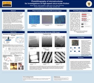
SlideShare a Scribd company logo
Abstract
Apparatus
Photolithography Process
Summary
What determines the friction and wear between two objects in
sliding contact? Although Da Vinci, Amontons and Coulomb
discovered the classical laws of friction centuries ago, this
question remains a puzzle for researchers seeking to
understand friction at the atomic level. Rapid progress has been
made over the last thirty years with the arrival of experimental
techniques capable of probing surface forces on ever smaller
length scales. These advances promise to help solve the
technical challenges currently plaguing the development of
microscopic machines. The devices, known as
microelectromechanical systems (MEMS), may serve as the
mechanical counterpart to integrated circuits, but progress
remains slow as structural materials and lubricant strategies
continue to be developed.
We discuss experiments in which a microscale probe and a
resonating disk of single-crystal quartz are put into contact to
replicate the sliding conditions found inside micromachines,
with rough contacts, high shear speeds, and lubricant films only
one molecule thick. This semester, we learned and implemented
a method for fabricating microscale structures with ultraviolet
photolithography. Characterization of the structures using
optical and electron microscopies played a key role in
optimizing our procedures. The fabricated features will serve
both as test sites for friction studies and as location markers to
enable post-test, ex-situ wear analysis..
Photolithography of microstructures
for investigations of high-speed micro-scale friction
Kieran Berton, Kali Gustafson, Halle Hund, Prof. Brian Borovsky
Physics Department, St. Olaf College, Northfield, MN
Acknowledgements
We gratefully acknowledge Jay Demas and his DUR group, Eric Cole, Elliot Schmidt, and Greg Cibuzar
and Jim Marti from the Minnesota Nano Center for helpful discussions, assistance, and technical
expertise.
References1. Brian Borovsky, Adam Booth, and Erin Manlove, Applied Physics Letters 91, 114101 (2007).
2. B. Borovsky, J. Krim, S. A. Syed Asif, and K. J. Wahl, Journal of Applied Physics 90, 6391 (2001).
3. B. Borovsky, B. Mason, and J. Krim, Journal of Applied Physics 88, 4017 (2000).
4. Top Image Courtesy of Nanorian Technologies: http://www.nanoriantech.com/photolitography/.
Bottom Image Courtesy of MNX: MEMS and Nanotechnology Exchange: https://www.mems-
exchange.org/MEMS/processes/lithography.html.
5 µm
Phase Contrast and Dissecting Microscope Images
Scanning Electron Microscope (SEM) Images
Future Work
Nanoindenter and Quartz Crystal Microbalance1,2
(NI-QCM)
Replicating contacts in
microdevices:
• Small contact radii: ~1 µm
• Fast sliding speeds: ~1 m/s
• Randomly rough surfaces
• Relevant materials and
lubricants
0 Tim
e
~30 min
Amplitude
0
50 nm
Amplitude at resonance is
ramped while normal load is
held fixed
Quartz resonance
curves
Far Right:
NI-QCM apparatus
and scanner base.
Near Right:
Close-up of
microsphere tip
with reflection on
electrode surface.
~0.02”
Measurement technique: Changes in the resonant frequency and
quality factor of the quartz disk (upon contact with the tip) are
determined as functions of oscillation amplitude, at a fixed normal
load.
fres

Change in resonant frequency upon contact with
the tip
Change in half bandwidth upon contact with the tip
1
2
resQ f
  
  
 
Change in inverse quality factor (dissipation)
0 1.4( / ) peakU pm V Q V  
Transverse oscillation amplitude of the
quartz surface is determined from the peak
drive voltage Vpeak.3
50 µm diameter
Gold electrode, with
organic monolayer
(octadecanethiol)
Aluminum oxide probe
30 second UV-light
exposure
(phase contrast)
33 second UV-light exposure
(dissecting)
34 second UV-light exposure
(phase contrast)
Topographic Mode
30 second UV-light
exposure
32 second UV-light
exposure
33 second UV-light
exposure
Full Mode
30 second UV-light
exposure
32 second UV-light
exposure
33 second UV-light
exposure
Scanning electron microscope (SEM) images were taken using the two modes shown above. An electron beam
interacts with atoms in the sample, producing various signals that contain information about the sample’s
surface topography and composition. In topographic mode, one electron beam is directed at the sample to
produce information about the sample’s surface topography. In full mode, two electron beams allow us to
characterize the sample’s composition.
We prepared the crystal by
cleaning it with isopropyl in a
10 minute ultrasonic bath. The
quartz crystal was then dried
with nitrogen and spin coated
with the photoresist for 30
seconds at 3000 RPM. The
prebake consists of a 1
minute, 105°C hardening of
the substrate. We then placed
our photomask over the
sample and exposed both to
UV-light at various time
increments. To develop, we
agitated the exposed crystal in
the microposit for 50 seconds
and then quenched the
developing process by setting
the crystal in DI water for 2
minutes. To set the
microstructures the we “hard-
baked” the crystal for 20
minutes at 120°C.
We used S1805 Photoresist and Microposit
351, which were both obtained from the
Minnesota Nano Center.
Now that we have refined the
fabrication process to
produce micro structures with
straight edges, we look ahead
to make structures which will
be more suited to our friction
testing goals. 2x2 micron
squares with a 20 micron
pitch will allow us to reliably
use the nanoindenter to
scrape both a structure and
the bare crystal with every
friction test. We hope to use
these structures in order to
know where we have
performed a friction test. In
future research, we also plan
to coat the crystal in a various
thin films to characterize how
the films affect friction
testing.
Preparation process4
Our goal this semester was to optimize the photolithographic
fabrication process to successfully create micro structures with
straight edges atop our gold-film quartz crystals. We varied
parameters such as UV-light exposure, microposit development,
and photoresist coating. Through experimentation, we
determined that a UV-light exposure time of 33 seconds, a
microposit development of 50 seconds, and a photoresist
coating of 30 seconds at 3000 RPM optimized the structures.
Informed by what we learned, we hope to perform friction tests
on our microstructures and continue to refine our
photolithographic development process.

More Related Content

What's hot

Nano 101: A Review of the Art and Science of Nanotechnology
Nano 101: A Review of the Art and Science of NanotechnologyNano 101: A Review of the Art and Science of Nanotechnology
Nano 101: A Review of the Art and Science of Nanotechnology
Triumvirate Environmental
 
Nano kolkata
Nano kolkataNano kolkata
Nano kolkata
Rakesh Khandal
 
Nanotechnology20120918 19-26 lecture 4-5-6 - Nanomaterials
Nanotechnology20120918  19-26 lecture 4-5-6 - NanomaterialsNanotechnology20120918  19-26 lecture 4-5-6 - Nanomaterials
Nanotechnology20120918 19-26 lecture 4-5-6 - Nanomaterials
Chin Yung Jyi
 
Characterization of nanopartical
Characterization of nanoparticalCharacterization of nanopartical
Characterization of nanopartical
Amany EL-Hallaq
 
SYNTHESIS AND CHARACTERIZATION OF ZNO NANO STRUCTURES BY MICROWAVE-ASSISTED T...
SYNTHESIS AND CHARACTERIZATION OF ZNO NANO STRUCTURES BY MICROWAVE-ASSISTED T...SYNTHESIS AND CHARACTERIZATION OF ZNO NANO STRUCTURES BY MICROWAVE-ASSISTED T...
SYNTHESIS AND CHARACTERIZATION OF ZNO NANO STRUCTURES BY MICROWAVE-ASSISTED T...
Mathankumar S
 
Nano Tech Lecture1 Dr. A.Waheed Anwar
Nano Tech Lecture1 Dr. A.Waheed AnwarNano Tech Lecture1 Dr. A.Waheed Anwar
Nano Tech Lecture1 Dr. A.Waheed Anwar
Engr Mansoor Mirza
 
Study of magnetic and structural and optical properties of Zn doped Fe3O4 nan...
Study of magnetic and structural and optical properties of Zn doped Fe3O4 nan...Study of magnetic and structural and optical properties of Zn doped Fe3O4 nan...
Study of magnetic and structural and optical properties of Zn doped Fe3O4 nan...
Nanomedicine Journal (NMJ)
 
Nanoscience MPhys Final Year Research Project Poster Presentation
Nanoscience MPhys Final Year Research Project Poster PresentationNanoscience MPhys Final Year Research Project Poster Presentation
Nanoscience MPhys Final Year Research Project Poster Presentation
Jakub Lewandowski
 
Nano materials
Nano materialsNano materials
Nano materials
Sahil Anande
 
Nanotechnology
NanotechnologyNanotechnology
Nanotechnology
Andrew
 
nanomaterial and dimensional effect
nanomaterial and dimensional effect nanomaterial and dimensional effect
nanomaterial and dimensional effect
sameerr98
 
INTRODUCTION TO NANOMATERIALS - by A. Alagarasi
INTRODUCTION TO NANOMATERIALS - by A. AlagarasiINTRODUCTION TO NANOMATERIALS - by A. Alagarasi
INTRODUCTION TO NANOMATERIALS - by A. Alagarasi
Chand Sukumar
 
Nanomaterials dr.surendran prambadath
Nanomaterials dr.surendran prambadathNanomaterials dr.surendran prambadath
Nanomaterials dr.surendran prambadath
Surendran Parambadath
 
Nanotechnology overview final
Nanotechnology overview finalNanotechnology overview final
Nanotechnology overview final
Manoranjan Ghosh
 
Seminar ppt
Seminar pptSeminar ppt
Unique Properties At The Nanoscale
Unique Properties At The NanoscaleUnique Properties At The Nanoscale
Unique Properties At The Nanoscale
Lionel Wolberger
 
Properties of Nano-materials
Properties of Nano-materialsProperties of Nano-materials
Properties of Nano-materials
Partha P. Mishra
 
Doping the quantum dots
Doping the quantum dotsDoping the quantum dots
Doping the quantum dots
Ahmad Aly
 
MAster's Thesis presentation
MAster's Thesis presentationMAster's Thesis presentation
MAster's Thesis presentation
Nazanin Karimi
 

What's hot (19)

Nano 101: A Review of the Art and Science of Nanotechnology
Nano 101: A Review of the Art and Science of NanotechnologyNano 101: A Review of the Art and Science of Nanotechnology
Nano 101: A Review of the Art and Science of Nanotechnology
 
Nano kolkata
Nano kolkataNano kolkata
Nano kolkata
 
Nanotechnology20120918 19-26 lecture 4-5-6 - Nanomaterials
Nanotechnology20120918  19-26 lecture 4-5-6 - NanomaterialsNanotechnology20120918  19-26 lecture 4-5-6 - Nanomaterials
Nanotechnology20120918 19-26 lecture 4-5-6 - Nanomaterials
 
Characterization of nanopartical
Characterization of nanoparticalCharacterization of nanopartical
Characterization of nanopartical
 
SYNTHESIS AND CHARACTERIZATION OF ZNO NANO STRUCTURES BY MICROWAVE-ASSISTED T...
SYNTHESIS AND CHARACTERIZATION OF ZNO NANO STRUCTURES BY MICROWAVE-ASSISTED T...SYNTHESIS AND CHARACTERIZATION OF ZNO NANO STRUCTURES BY MICROWAVE-ASSISTED T...
SYNTHESIS AND CHARACTERIZATION OF ZNO NANO STRUCTURES BY MICROWAVE-ASSISTED T...
 
Nano Tech Lecture1 Dr. A.Waheed Anwar
Nano Tech Lecture1 Dr. A.Waheed AnwarNano Tech Lecture1 Dr. A.Waheed Anwar
Nano Tech Lecture1 Dr. A.Waheed Anwar
 
Study of magnetic and structural and optical properties of Zn doped Fe3O4 nan...
Study of magnetic and structural and optical properties of Zn doped Fe3O4 nan...Study of magnetic and structural and optical properties of Zn doped Fe3O4 nan...
Study of magnetic and structural and optical properties of Zn doped Fe3O4 nan...
 
Nanoscience MPhys Final Year Research Project Poster Presentation
Nanoscience MPhys Final Year Research Project Poster PresentationNanoscience MPhys Final Year Research Project Poster Presentation
Nanoscience MPhys Final Year Research Project Poster Presentation
 
Nano materials
Nano materialsNano materials
Nano materials
 
Nanotechnology
NanotechnologyNanotechnology
Nanotechnology
 
nanomaterial and dimensional effect
nanomaterial and dimensional effect nanomaterial and dimensional effect
nanomaterial and dimensional effect
 
INTRODUCTION TO NANOMATERIALS - by A. Alagarasi
INTRODUCTION TO NANOMATERIALS - by A. AlagarasiINTRODUCTION TO NANOMATERIALS - by A. Alagarasi
INTRODUCTION TO NANOMATERIALS - by A. Alagarasi
 
Nanomaterials dr.surendran prambadath
Nanomaterials dr.surendran prambadathNanomaterials dr.surendran prambadath
Nanomaterials dr.surendran prambadath
 
Nanotechnology overview final
Nanotechnology overview finalNanotechnology overview final
Nanotechnology overview final
 
Seminar ppt
Seminar pptSeminar ppt
Seminar ppt
 
Unique Properties At The Nanoscale
Unique Properties At The NanoscaleUnique Properties At The Nanoscale
Unique Properties At The Nanoscale
 
Properties of Nano-materials
Properties of Nano-materialsProperties of Nano-materials
Properties of Nano-materials
 
Doping the quantum dots
Doping the quantum dotsDoping the quantum dots
Doping the quantum dots
 
MAster's Thesis presentation
MAster's Thesis presentationMAster's Thesis presentation
MAster's Thesis presentation
 

Similar to Final Poster

Traineeship Melbourne University - Michael Beljaars
Traineeship Melbourne University - Michael BeljaarsTraineeship Melbourne University - Michael Beljaars
Traineeship Melbourne University - Michael Beljaars
Michael Beljaars
 
Analysis Of Carbon Nanotubes And Quantum Dots In A Photovoltaic Device
Analysis Of Carbon Nanotubes And Quantum Dots In A Photovoltaic DeviceAnalysis Of Carbon Nanotubes And Quantum Dots In A Photovoltaic Device
Analysis Of Carbon Nanotubes And Quantum Dots In A Photovoltaic Device
M. Faisal Halim
 
A Systematic Review on MEMS Gyroscope
A Systematic Review on MEMS GyroscopeA Systematic Review on MEMS Gyroscope
A Systematic Review on MEMS Gyroscope
ArjunKapoor65
 
A Systematic Review on MEMS Gyroscope.docx
A Systematic Review on MEMS Gyroscope.docxA Systematic Review on MEMS Gyroscope.docx
A Systematic Review on MEMS Gyroscope.docx
ArjunKapoor64
 
W03301330140
W03301330140W03301330140
W03301330140
ijceronline
 
Ultra smooth and lattice relaxed zn o thin films [eid]
Ultra smooth and lattice relaxed zn o thin films [eid]Ultra smooth and lattice relaxed zn o thin films [eid]
Ultra smooth and lattice relaxed zn o thin films [eid]
Eid Elsayed
 
OpticsExpress_Afshin
OpticsExpress_AfshinOpticsExpress_Afshin
OpticsExpress_Afshin
Afshin Ghaffari
 
scanning electron microscope
scanning electron microscopescanning electron microscope
scanning electron microscope
DrAkhilaCNV
 
Electron Microscopy Principle and Application
Electron Microscopy Principle and ApplicationElectron Microscopy Principle and Application
Electron Microscopy Principle and Application
KARTHIK REDDY C A
 
Surface patterns of inorganic nanoparticles characterized with atomic force m...
Surface patterns of inorganic nanoparticles characterized with atomic force m...Surface patterns of inorganic nanoparticles characterized with atomic force m...
Surface patterns of inorganic nanoparticles characterized with atomic force m...
Denzel Alexander
 
PolyMEMS INAOE, a Surface Micromachining Fabrication Module and the Developm...
PolyMEMS INAOE, a Surface Micromachining Fabrication Module  and the Developm...PolyMEMS INAOE, a Surface Micromachining Fabrication Module  and the Developm...
PolyMEMS INAOE, a Surface Micromachining Fabrication Module and the Developm...
José Andrés Alanís Navarro
 
Nanotechnology and display applications.pdf
Nanotechnology and display applications.pdfNanotechnology and display applications.pdf
Nanotechnology and display applications.pdf
NirmalM15
 
3 d molding and casting4
3 d molding and casting43 d molding and casting4
3 d molding and casting4
Fab Lab LIMA
 
Photonic Materials
Photonic MaterialsPhotonic Materials
Photonic Materials
Gaurav Singh Chandel
 
Viii. molecular electronics and nanoscience
Viii. molecular electronics and nanoscienceViii. molecular electronics and nanoscience
Viii. molecular electronics and nanoscience
AllenHermann
 
Transmission Electron Microscope
Transmission Electron MicroscopeTransmission Electron Microscope
Transmission Electron Microscope
20was
 
Lab module sem
Lab module semLab module sem
Lab module sem
Banjuraizah Johar
 
Nanomedicine 2005
Nanomedicine 2005Nanomedicine 2005
Nanomedicine 2005
Dr. Mashiur Rahman
 
Mems technology
Mems technologyMems technology
Mems technology
amit parcha
 
Skt mems
Skt memsSkt mems
Skt mems
Sama Khan
 

Similar to Final Poster (20)

Traineeship Melbourne University - Michael Beljaars
Traineeship Melbourne University - Michael BeljaarsTraineeship Melbourne University - Michael Beljaars
Traineeship Melbourne University - Michael Beljaars
 
Analysis Of Carbon Nanotubes And Quantum Dots In A Photovoltaic Device
Analysis Of Carbon Nanotubes And Quantum Dots In A Photovoltaic DeviceAnalysis Of Carbon Nanotubes And Quantum Dots In A Photovoltaic Device
Analysis Of Carbon Nanotubes And Quantum Dots In A Photovoltaic Device
 
A Systematic Review on MEMS Gyroscope
A Systematic Review on MEMS GyroscopeA Systematic Review on MEMS Gyroscope
A Systematic Review on MEMS Gyroscope
 
A Systematic Review on MEMS Gyroscope.docx
A Systematic Review on MEMS Gyroscope.docxA Systematic Review on MEMS Gyroscope.docx
A Systematic Review on MEMS Gyroscope.docx
 
W03301330140
W03301330140W03301330140
W03301330140
 
Ultra smooth and lattice relaxed zn o thin films [eid]
Ultra smooth and lattice relaxed zn o thin films [eid]Ultra smooth and lattice relaxed zn o thin films [eid]
Ultra smooth and lattice relaxed zn o thin films [eid]
 
OpticsExpress_Afshin
OpticsExpress_AfshinOpticsExpress_Afshin
OpticsExpress_Afshin
 
scanning electron microscope
scanning electron microscopescanning electron microscope
scanning electron microscope
 
Electron Microscopy Principle and Application
Electron Microscopy Principle and ApplicationElectron Microscopy Principle and Application
Electron Microscopy Principle and Application
 
Surface patterns of inorganic nanoparticles characterized with atomic force m...
Surface patterns of inorganic nanoparticles characterized with atomic force m...Surface patterns of inorganic nanoparticles characterized with atomic force m...
Surface patterns of inorganic nanoparticles characterized with atomic force m...
 
PolyMEMS INAOE, a Surface Micromachining Fabrication Module and the Developm...
PolyMEMS INAOE, a Surface Micromachining Fabrication Module  and the Developm...PolyMEMS INAOE, a Surface Micromachining Fabrication Module  and the Developm...
PolyMEMS INAOE, a Surface Micromachining Fabrication Module and the Developm...
 
Nanotechnology and display applications.pdf
Nanotechnology and display applications.pdfNanotechnology and display applications.pdf
Nanotechnology and display applications.pdf
 
3 d molding and casting4
3 d molding and casting43 d molding and casting4
3 d molding and casting4
 
Photonic Materials
Photonic MaterialsPhotonic Materials
Photonic Materials
 
Viii. molecular electronics and nanoscience
Viii. molecular electronics and nanoscienceViii. molecular electronics and nanoscience
Viii. molecular electronics and nanoscience
 
Transmission Electron Microscope
Transmission Electron MicroscopeTransmission Electron Microscope
Transmission Electron Microscope
 
Lab module sem
Lab module semLab module sem
Lab module sem
 
Nanomedicine 2005
Nanomedicine 2005Nanomedicine 2005
Nanomedicine 2005
 
Mems technology
Mems technologyMems technology
Mems technology
 
Skt mems
Skt memsSkt mems
Skt mems
 

Final Poster

  • 1. Abstract Apparatus Photolithography Process Summary What determines the friction and wear between two objects in sliding contact? Although Da Vinci, Amontons and Coulomb discovered the classical laws of friction centuries ago, this question remains a puzzle for researchers seeking to understand friction at the atomic level. Rapid progress has been made over the last thirty years with the arrival of experimental techniques capable of probing surface forces on ever smaller length scales. These advances promise to help solve the technical challenges currently plaguing the development of microscopic machines. The devices, known as microelectromechanical systems (MEMS), may serve as the mechanical counterpart to integrated circuits, but progress remains slow as structural materials and lubricant strategies continue to be developed. We discuss experiments in which a microscale probe and a resonating disk of single-crystal quartz are put into contact to replicate the sliding conditions found inside micromachines, with rough contacts, high shear speeds, and lubricant films only one molecule thick. This semester, we learned and implemented a method for fabricating microscale structures with ultraviolet photolithography. Characterization of the structures using optical and electron microscopies played a key role in optimizing our procedures. The fabricated features will serve both as test sites for friction studies and as location markers to enable post-test, ex-situ wear analysis.. Photolithography of microstructures for investigations of high-speed micro-scale friction Kieran Berton, Kali Gustafson, Halle Hund, Prof. Brian Borovsky Physics Department, St. Olaf College, Northfield, MN Acknowledgements We gratefully acknowledge Jay Demas and his DUR group, Eric Cole, Elliot Schmidt, and Greg Cibuzar and Jim Marti from the Minnesota Nano Center for helpful discussions, assistance, and technical expertise. References1. Brian Borovsky, Adam Booth, and Erin Manlove, Applied Physics Letters 91, 114101 (2007). 2. B. Borovsky, J. Krim, S. A. Syed Asif, and K. J. Wahl, Journal of Applied Physics 90, 6391 (2001). 3. B. Borovsky, B. Mason, and J. Krim, Journal of Applied Physics 88, 4017 (2000). 4. Top Image Courtesy of Nanorian Technologies: http://www.nanoriantech.com/photolitography/. Bottom Image Courtesy of MNX: MEMS and Nanotechnology Exchange: https://www.mems- exchange.org/MEMS/processes/lithography.html. 5 µm Phase Contrast and Dissecting Microscope Images Scanning Electron Microscope (SEM) Images Future Work Nanoindenter and Quartz Crystal Microbalance1,2 (NI-QCM) Replicating contacts in microdevices: • Small contact radii: ~1 µm • Fast sliding speeds: ~1 m/s • Randomly rough surfaces • Relevant materials and lubricants 0 Tim e ~30 min Amplitude 0 50 nm Amplitude at resonance is ramped while normal load is held fixed Quartz resonance curves Far Right: NI-QCM apparatus and scanner base. Near Right: Close-up of microsphere tip with reflection on electrode surface. ~0.02” Measurement technique: Changes in the resonant frequency and quality factor of the quartz disk (upon contact with the tip) are determined as functions of oscillation amplitude, at a fixed normal load. fres  Change in resonant frequency upon contact with the tip Change in half bandwidth upon contact with the tip 1 2 resQ f         Change in inverse quality factor (dissipation) 0 1.4( / ) peakU pm V Q V   Transverse oscillation amplitude of the quartz surface is determined from the peak drive voltage Vpeak.3 50 µm diameter Gold electrode, with organic monolayer (octadecanethiol) Aluminum oxide probe 30 second UV-light exposure (phase contrast) 33 second UV-light exposure (dissecting) 34 second UV-light exposure (phase contrast) Topographic Mode 30 second UV-light exposure 32 second UV-light exposure 33 second UV-light exposure Full Mode 30 second UV-light exposure 32 second UV-light exposure 33 second UV-light exposure Scanning electron microscope (SEM) images were taken using the two modes shown above. An electron beam interacts with atoms in the sample, producing various signals that contain information about the sample’s surface topography and composition. In topographic mode, one electron beam is directed at the sample to produce information about the sample’s surface topography. In full mode, two electron beams allow us to characterize the sample’s composition. We prepared the crystal by cleaning it with isopropyl in a 10 minute ultrasonic bath. The quartz crystal was then dried with nitrogen and spin coated with the photoresist for 30 seconds at 3000 RPM. The prebake consists of a 1 minute, 105°C hardening of the substrate. We then placed our photomask over the sample and exposed both to UV-light at various time increments. To develop, we agitated the exposed crystal in the microposit for 50 seconds and then quenched the developing process by setting the crystal in DI water for 2 minutes. To set the microstructures the we “hard- baked” the crystal for 20 minutes at 120°C. We used S1805 Photoresist and Microposit 351, which were both obtained from the Minnesota Nano Center. Now that we have refined the fabrication process to produce micro structures with straight edges, we look ahead to make structures which will be more suited to our friction testing goals. 2x2 micron squares with a 20 micron pitch will allow us to reliably use the nanoindenter to scrape both a structure and the bare crystal with every friction test. We hope to use these structures in order to know where we have performed a friction test. In future research, we also plan to coat the crystal in a various thin films to characterize how the films affect friction testing. Preparation process4 Our goal this semester was to optimize the photolithographic fabrication process to successfully create micro structures with straight edges atop our gold-film quartz crystals. We varied parameters such as UV-light exposure, microposit development, and photoresist coating. Through experimentation, we determined that a UV-light exposure time of 33 seconds, a microposit development of 50 seconds, and a photoresist coating of 30 seconds at 3000 RPM optimized the structures. Informed by what we learned, we hope to perform friction tests on our microstructures and continue to refine our photolithographic development process.