
Recommended
More Related Content
What's hot
What's hot (18)
Similar to Architecture of 8085
Similar to Architecture of 8085 (20)
More from HarshitParkar6677
More from HarshitParkar6677 (20)
Recently uploaded
Recently uploaded (20)
Architecture of 8085
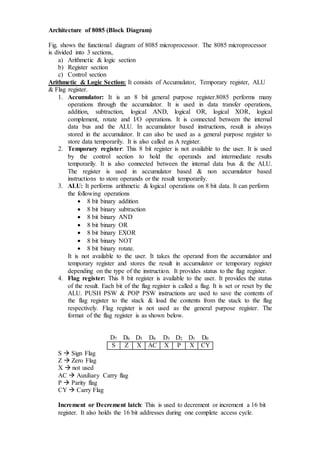
- 1. Architecture of 8085 (Block Diagram) Fig. shows the functional diagram of 8085 microprocessor. The 8085 microprocessor is divided into 3 sections, a) Arithmetic & logic section b) Register section c) Control section Arithmetic & Logic Section: It consists of Accumulator, Temporary register, ALU & Flag register. 1. Accumulator: It is an 8 bit general purpose register.8085 performs many operations through the accumulator. It is used in data transfer operations, addition, subtraction, logical AND, logical OR, logical XOR, logical complement, rotate and I/O operations. It is connected between the internal data bus and the ALU. In accumulator based instructions, result is always stored in the accumulator. It can also be used as a general purpose register to store data temporarily. It is also called as A register. 2. Temporary register: This 8 bit register is not available to the user. It is used by the control section to hold the operands and intermediate results temporarily. It is also connected between the internal data bus & the ALU. The register is used in accumulator based & non accumulator based instructions to store operands or the result temporarily. 3. ALU: It performs arithmetic & logical operations on 8 bit data. It can perform the following operations 8 bit binary addition 8 bit binary subtraction 8 bit binary AND 8 bit binary OR 8 bit binary EXOR 8 bit binary NOT 8 bit binary rotate. It is not available to the user. It takes the operand from the accumulator and temporary register and stores the result in accumulator or temporary register depending on the type of the instruction. It provides status to the flag register. 4. Flag register: This 8 bit register is available to the user. It provides the status of the result. Each bit of the flag register is called a flag. It is set or reset by the ALU. PUSH PSW & POP PSW instructions are used to save the contents of the flag register to the stack & load the contents from the stack to the flag respectively. Flag register is not used as the general purpose register. The format of the flag register is as shown below. D7 D6 D5 D4 D3 D2 D1 D0 S Z X AC X P X CY S Sign Flag Z Zero Flag X not used AC Auxiliary Carry flag P Parity flag CY Carry Flag Increment or Decrement latch: This is used to decrement or increment a 16 bit register. It also holds the 16 bit addresses during one complete access cycle.
- 2. Address buffer: It is used to drive the higher order unidirectional address bus (A8 – A15). It is a tristate 8 bit buffer. Data/Address buffer: It consists of 2 channel 8 bit multiplexers and buffers. It multiplexes internal data bus (D0 – D7) with low order address bus (A0 – A7). Control Section: It performs data transfer and decision making operations. It consists of an instruction register, instruction decoder, timing & control circuit, clock generator, interrupt controller and a serial I/O controller. 1. Instruction register: It is an 8 bit register used to hold an opcode (operation code or hex code) of the current instruction. During instruction fetch operations, 8085 fetches the first byte of the opcode into the instruction register. This is not available to the user. 2. Instruction decoder: This decodes the contents of the instruction register. It can recognize only 74 instructions. It also determines the number of fetch cycles required to fetch the current instruction by decoding the opcode. It also sends the encoded information to the timing and control logic circuit. 3. Timing & Control logic: It is a synchronous sequential circuit. It controls all the internal (ALU, flag register etc.) and external (memory, I/O) units. It performs all the micro operations required to fetch and execute the current instruction. 4. Clock generator: It consists of an amplifier or a buffer. It generates 50% duty cycle, with a 2 phase TTL clock. It requires external clock generator (crystal oscillator, RC or LC circuit), and it also synchronizes RESET & READY signals. 5. Interrupt control: It controls all operations of five interrupts TRAP, RST7.5, RST6.5, RST5.5 and INTR. It also generates signal. It also maintains priority among all interrupts. It consists of flip-flops and logic gates. INTR is an active high, level triggered general purpose hardware interrupt. When INTR occurs, the microprocessor generates INTA. TRAP is an active high, edge and level triggered non-maskable (NMI) highest priority hardware interrupt. When TRAP occurs, the microprocessor starts execution from 0024H automatically. Restart Interrupt RST7.5 is a level trggered , RST 6.5, RST5.5 are edge triggered interrupt, which are active high, maskable interrupt. When these are invoked, the microprocessor transfers the program control to vector address 003CH, 0034H and 002CH respectively. 6. Serial I/O control: It consists of serial input and serial output ports. It transmits or receives data. The pins SID and SOD are used for serial input and output operations respectively. Registerorganization: It consists of 3 types of registers 1. Temporary registers 2. General purpose register 3. Special purpose register 1. Temporary registers: 8085 microprocessor provides two 8 bit temporary registers W & Z. These registers are not available to the user. They are used by the control sections to hold the address of the program memory, data memory and intermediate data temporarily. INTA
- 3. 2. General Purpose registers: 8085 microprocessor provides only 6 eight bit general purpose register, B, C, D, E, H and L. These registers are available for the user. These are used to hold 8 bit operands in 8 bit operations. A pair of two 8 bit registers such as BC, DE, and HL can be used with 16 bit operations. 3. Special purpose registers: 8085 provides two 16 bit special purpose registers, Program Counter & Stack Pointer a. Program Counter (PC): It is a 16 bit register used to hold the address of the next instruction to be executed by the processor. It is automatically incremented by the control section during the instruction fetch operations. After fetching all bytes of the current instruction, the control section stops incrementing the program Counter & waits for the execution. The contents of the PC can be changed with branch instruction & few special instructions. The RESET signal clears the PC. b. Stack pointer (SP): It is a 16 bit register. It is used to access Stack memory in LIFO mode. The 8085 microprocessor always stores bytes on the stack from the highest address (top) to lowest address i.e., the stack is grown from top. It is always used to point to the stack memory locations. It is never used to point to Data or Program memory locations. During stack write operations, the control section decrements the SP by 1 and then stores one byte at a new stack location. During stack read operation, the control section reads a byte from the top of the stack and then increments the SP to point to the next lower stack location. Hence SP must be initialized with the highest address of the stack memory. Limitations of 8 bit microprocessors: The word length is 8 bit, hence the processing speed is low Most of the 8 bit microprocessors are non-pipelined (reads one instruction at at a time), hence poor performance. The instruction set is limited (74), hence processing power is less. Due to 16bits address lines, only 64Kbytes can be accessed. Hence IBM PC cannot make use of 8085 (requires minimum 640KB) Since multiplexed address and data bus is used, extra hardware required to separate the signals. Provides very few addressing modes, hence the instruction set is not flexible. It is very difficult to design a compiler for an 8 bit microprocessor. Limited number of flags (5). Limited number of Interrupts. (5) It cannot be used in scientific calculations. It does not handle real numbers. It cannot be used in multiprocessor systems. Number of input/output devices possible to connect are only 256 (Since 8bit I/O address)