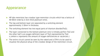
Mersistor
Sandeep Ratakonda
Yamini Krishna Kunduru
Index
 Manufacturing
 Working
 Operation
 Transistor vs Memristor
 Applications
 Challenges
Manufacturing
 Fabricators could use same chip fabrication plats that are used to fabricate
CMOS chips.
 There is no need to take up expensive retooling or new construction.
 Titanium dioxide can be manufactured in any semiconductor fab currently in
use.
Schematic of fabrication approach.
Manufacturing(cont.)
 Crossbar architecture is the widely used architecture for the fabrication of a
memristor.
 The main advantages of the cross bar architecture is that it is well ordered,
periodic and simple structure.
 But the problem is that designing the crossbar architecture in nanoscale
resolutions, the standard lithography techniques are insufficient.
 HP while manufacturing the memristor used the nanoimprint lithography which
uses a stamp like structure with nanometer resolution.
 Nanoscale fabrication approaches can include self-assembly techniques in which
polymers or other materials can form periodic structures on a surface based
process of energy minimalization.
 The self assembly techniques can be used to form a periodic mask structure over a
metal film.
Images of 1 X 21 array of memristors
A. Optical microscope image.
B. Scanning Electron Microscope image of the junction area.
C. Atomic Force Microscope image of part of the array.
Appearance
 HP labs memristor has crossbar type memristor circuits which has a lattice of
40-50nm wide by 2-3nm thick platinum wires.
 The top and bottom layer are separated by a switching element
approximately 3-30nm in thickness.
 The switching element has two equal parts of titanium dioxide(Tio2).
 The layer connected to the bottom platinum wire is initially perfect Tio2 and
the other half is an oxygen deficient layer of Tio2 represented by Tio2-
x.(where x represents the amount of oxygen deficiencies or vacancies.)
 The entire circuit cannot be seen by the naked and a STM is to be used to
visualize the physical setup of the crossbar design of the memristor circuit.
Crossbar architecture and magnified
Memristive switch
Operation of Memristor
 Memristors operation can be explained in three steps
 1. application of power or more importantly current to the memristor.
 2. amount of time the current flows across the crossbar gap and how the
titanium dioxide cube converts to a conductor from a semiconductor.
 3. Actual memory of the cube that can be read as data.
Step 1
 In the Memristor circuit, two wires are selected to apply power either in a
positive or negative direction.
 if connected in positive direction will attempt to close the switch and if the
connection is in negative direction will attempt to an open switch.
 Apllying of power will be able to completely open the circuit between the
wires but it is not able to completely close the circuit since the material is
still semi-conductor by nature.
 Power can be placed on certain wires to open and close the switches in the
memristor.
Step 2
 In the second step it involves the atomic process that the gap material, made from
Tio2,that opens and closes the switch
 At this initial state of gap is neutral meaning that it consists of one half of pure
Tio2 and other half consists of Tio2 with oxygen deficiencies(Tio2-x).
 Where thave value of x is 0.05 initially, when the positive charge is applied to the
Tio2-x, the deficiencies were poshed towards the Tio2
 This makes the resistance in the gap to drop, and the memristor becomes more
conductive and there is a rise in the current.
 And if an inverse current is applied the deficiencies are withdrawn into the Tio2-x
region and this increases the gap and there is a rise in the resistance.
 When there is a rise in the current the switch is considered as HIgh and data
purpose as binary 1
 And when the current is dropped the switch is LOW and it is considered as binary 0
Diffusing of Oxygen
A) Tio2-x layer having oxygen deficiencies over insulating Tio2 layer
B) Positive voltage applied to top layer repels oxygen deficiencies in to the insulating Tio2 layer below
C) Negative voltage on the switch attracts the positively charged oxygen bubbles pulling them out of the
Tio2.
Step 3
 When power is no longer applied to the switch the oxygen vacancies remain in
the same position before the power was shutdown .
 This means that the value of the resistance of the material gap will remain
indefinitely till the power is applied back .
 This means that the memristor circuits are infact storing data physically .
 If we want the positive voltage to turn the memristor off Tio2-x layer should
be on the top .
 If we want the positive voltage to turn on the memristor then Tio2 layer
should be on the top .
 In the initial stage memristor has only open switches and no information is
stored, when you start closing switches we can store vast amounts of data
compactly and efficiently
Transistor vs Memristor
Transistor Memristor
1. Three terminal device
2. Stores data by electron charge
3. Requires a power source to retain a
data state
4. Capable of performing analog or
digital functions depending on
applied biased voltages
1. Two terminal device
2. Stores data by resistance state
3. Does not require a power source to
retain a data state
4. Capable of performing analog or
digital functions depending on a
particular material used for
memristor
Applications
 Non volatile memory
 Logic or computatuion
 Neuromorphic electronics
 Arithematic processing
 Pattern comparision etc.,
Materials used
 Although different memristor materials have their merits and demerits in
terms of the underlying physics, each material share the same resistance
switching .
 Variety of binary oxides such as WO3, Ir2O3,MoO3,RhO2 adjusted to have
memristive properties .
 A variety of other memristor variations based on TiO,CuO,NiO, and HfO
materials are under experimental investigationfor the past several years
Challenges
 Though hundreds of thousands of memristors have already been built , there
is still much to be perfected
 The memristor major challenges are it’s relatively low speeds and the need
for designers to learn how to build the circuits with new element.
 Dissipates heat when data being written or read
 No design standards
 Needs more defect engineering
References
 IEEE Spectrum: The Mysterious Memristor By Sally Adee
http://www.spectrum.ieee.org/may08/6207
 “How We Found the Missing Memristor” By R. Stanley Williams, December
2008 • IEEE Spectrum, www.spectrum.ieee.org
 http://newsvote.bbc.co.uk/mpapps/pagetools/email/news.bbc.co.uk/2/hi/t
echnology/7 377063.stm
 A hybrid nanomemristor/transistor logic circuit capable of self-programming
Julien Borghetti, Zhiyong Li, Joseph Straznicky, Xuema Li, Douglas A. A.
Ohlberg, Wei Wu, Duncan R. Stewart,and R. Stanley
Thank you.

Memristor 2

  • 1.
  • 2.
    Index  Manufacturing  Working Operation  Transistor vs Memristor  Applications  Challenges
  • 3.
    Manufacturing  Fabricators coulduse same chip fabrication plats that are used to fabricate CMOS chips.  There is no need to take up expensive retooling or new construction.  Titanium dioxide can be manufactured in any semiconductor fab currently in use. Schematic of fabrication approach.
  • 4.
    Manufacturing(cont.)  Crossbar architectureis the widely used architecture for the fabrication of a memristor.  The main advantages of the cross bar architecture is that it is well ordered, periodic and simple structure.  But the problem is that designing the crossbar architecture in nanoscale resolutions, the standard lithography techniques are insufficient.  HP while manufacturing the memristor used the nanoimprint lithography which uses a stamp like structure with nanometer resolution.  Nanoscale fabrication approaches can include self-assembly techniques in which polymers or other materials can form periodic structures on a surface based process of energy minimalization.  The self assembly techniques can be used to form a periodic mask structure over a metal film.
  • 5.
    Images of 1X 21 array of memristors A. Optical microscope image. B. Scanning Electron Microscope image of the junction area. C. Atomic Force Microscope image of part of the array.
  • 6.
    Appearance  HP labsmemristor has crossbar type memristor circuits which has a lattice of 40-50nm wide by 2-3nm thick platinum wires.  The top and bottom layer are separated by a switching element approximately 3-30nm in thickness.  The switching element has two equal parts of titanium dioxide(Tio2).  The layer connected to the bottom platinum wire is initially perfect Tio2 and the other half is an oxygen deficient layer of Tio2 represented by Tio2- x.(where x represents the amount of oxygen deficiencies or vacancies.)  The entire circuit cannot be seen by the naked and a STM is to be used to visualize the physical setup of the crossbar design of the memristor circuit.
  • 7.
    Crossbar architecture andmagnified Memristive switch
  • 8.
    Operation of Memristor Memristors operation can be explained in three steps  1. application of power or more importantly current to the memristor.  2. amount of time the current flows across the crossbar gap and how the titanium dioxide cube converts to a conductor from a semiconductor.  3. Actual memory of the cube that can be read as data.
  • 9.
    Step 1  Inthe Memristor circuit, two wires are selected to apply power either in a positive or negative direction.  if connected in positive direction will attempt to close the switch and if the connection is in negative direction will attempt to an open switch.  Apllying of power will be able to completely open the circuit between the wires but it is not able to completely close the circuit since the material is still semi-conductor by nature.  Power can be placed on certain wires to open and close the switches in the memristor.
  • 10.
    Step 2  Inthe second step it involves the atomic process that the gap material, made from Tio2,that opens and closes the switch  At this initial state of gap is neutral meaning that it consists of one half of pure Tio2 and other half consists of Tio2 with oxygen deficiencies(Tio2-x).  Where thave value of x is 0.05 initially, when the positive charge is applied to the Tio2-x, the deficiencies were poshed towards the Tio2  This makes the resistance in the gap to drop, and the memristor becomes more conductive and there is a rise in the current.  And if an inverse current is applied the deficiencies are withdrawn into the Tio2-x region and this increases the gap and there is a rise in the resistance.  When there is a rise in the current the switch is considered as HIgh and data purpose as binary 1  And when the current is dropped the switch is LOW and it is considered as binary 0
  • 11.
    Diffusing of Oxygen A)Tio2-x layer having oxygen deficiencies over insulating Tio2 layer B) Positive voltage applied to top layer repels oxygen deficiencies in to the insulating Tio2 layer below C) Negative voltage on the switch attracts the positively charged oxygen bubbles pulling them out of the Tio2.
  • 12.
    Step 3  Whenpower is no longer applied to the switch the oxygen vacancies remain in the same position before the power was shutdown .  This means that the value of the resistance of the material gap will remain indefinitely till the power is applied back .  This means that the memristor circuits are infact storing data physically .  If we want the positive voltage to turn the memristor off Tio2-x layer should be on the top .  If we want the positive voltage to turn on the memristor then Tio2 layer should be on the top .  In the initial stage memristor has only open switches and no information is stored, when you start closing switches we can store vast amounts of data compactly and efficiently
  • 13.
    Transistor vs Memristor TransistorMemristor 1. Three terminal device 2. Stores data by electron charge 3. Requires a power source to retain a data state 4. Capable of performing analog or digital functions depending on applied biased voltages 1. Two terminal device 2. Stores data by resistance state 3. Does not require a power source to retain a data state 4. Capable of performing analog or digital functions depending on a particular material used for memristor
  • 14.
    Applications  Non volatilememory  Logic or computatuion  Neuromorphic electronics  Arithematic processing  Pattern comparision etc.,
  • 15.
    Materials used  Althoughdifferent memristor materials have their merits and demerits in terms of the underlying physics, each material share the same resistance switching .  Variety of binary oxides such as WO3, Ir2O3,MoO3,RhO2 adjusted to have memristive properties .  A variety of other memristor variations based on TiO,CuO,NiO, and HfO materials are under experimental investigationfor the past several years
  • 16.
    Challenges  Though hundredsof thousands of memristors have already been built , there is still much to be perfected  The memristor major challenges are it’s relatively low speeds and the need for designers to learn how to build the circuits with new element.  Dissipates heat when data being written or read  No design standards  Needs more defect engineering
  • 17.
    References  IEEE Spectrum:The Mysterious Memristor By Sally Adee http://www.spectrum.ieee.org/may08/6207  “How We Found the Missing Memristor” By R. Stanley Williams, December 2008 • IEEE Spectrum, www.spectrum.ieee.org  http://newsvote.bbc.co.uk/mpapps/pagetools/email/news.bbc.co.uk/2/hi/t echnology/7 377063.stm  A hybrid nanomemristor/transistor logic circuit capable of self-programming Julien Borghetti, Zhiyong Li, Joseph Straznicky, Xuema Li, Douglas A. A. Ohlberg, Wei Wu, Duncan R. Stewart,and R. Stanley
  • 18.