SlideShare a Scribd company logo
General Description
The MAX6603 dual-channel, platinum RTD-to-voltage
signal conditioner excites and amplifies the signal from
two external 200Ω platinum-resistive temperature devices
(Pt RTD) to achieve high-voltage, level-filtered signals for
temperature measurements. The MAX6603 provides a
direct ratiometric output voltage to simplify the interface to
microcontrollers with integrated analog-to-digital convert-
ers (ADCs). External precision resistors and calibration
processes are not needed. The MAX6603 provides the
necessary signal-conditioning functions, including ratio-
metric excitation current, amplification, buffered voltage
outputs, diagnostic fault detections, and input protection.
The MAX6603 amplifies signals from two RTDs operat-
ing over the -40°C to +1000°C temperature range and
provides the temperature information as two independent
analog voltages. The MAX6603 features a ±6°C (max)
accuracy over the +400°C to +600°C temperature range.
The MAX6603 has overvoltage protection up to +16V on
RTD inputs, and ±5kV electrostatic discharge (ESD) pro-
tection at RTD input pins for reliable operation where RTD
temperature-sensing probes are used. The MAX6603
monitors the RTD for faults and asserts the respective DG
output low for fault conditions. The analog voltage outputs
can be readily connected to a variety of microcontrollers.
The MAX6603 is available in a small, 10-pin TDFN-EP
package and operates over the -40°C to +125°C automo-
tive temperature range from a single +3V to +5.5V power
supply.
Applications
●● Engine Control Management to Meet EURO IV
	Regulations
●● Braking Systems
●● Industrial Temperature Sensors
●● Food Transportation Monitoring Systems
●● Industrial Process Measurements
Features
●● Amplifies Pt RTD Temperature Signals
●● ±5kV ESD Protection on RTD Inputs
●● +16V Overvoltage Fault Protection on RTD Inputs
●● Low RTD Excitation Current Minimizes Self-Heating
Errors
●● Small, 10-Pin TDFN Package
●● Fully Ratiometric Operation
●● No Calibration Required for Standard RTDs
●● RTD Diagnostic Check
●● High Accuracy: ±6°C (max) from +400°C to +600°C
19-3975; Rev 1; 4/14
Note: Device is specified over the -40°C to +125°C tempera-
ture range.
*EP = Exposed pad.
+Denotes a lead(Pb)-free/RoHS-compliant package.
**Other base resistance values can be accommodated.
Contact the factory for more information.
PART PIN-PACKAGE RTD
PKG
CODE
MAX6603ATB+ 10 TDFN-EP* 200Ω** T1033-1
1
3
4
10+
8
7
OUT1
VCC
RS2+
RS1+
MAX6603
2 9 OUT2RS2-
5 6 GNDRS1-
TDFN
3mm x 3mm x 0.8mm
TOP VIEW
DG2
DG1
MAX6603 Dual-Channel, Platinum RTD-to-Voltage
Signal Conditioner
Pin Configuration
Ordering Information
EVALUATION KIT AVAILABLE
(All voltages referenced to GND, unless otherwise noted.)
VCC........................................................................-0.3V to +6.0V
RS1+, RS1-, RS2+, RS2-....................................-0.3V to +18.0V
OUT1, OUT2, DG1, DG2.......................... -0.3V to (VCC + 0.3V)
Continuous Power Dissipation (TA = +70°C)
10-Pin TDFN Single-Layer Board
(derate 18.5 mW/°C above +70°C).........................1481.5mW
10-Pin TDFN Multilayer Board
(derate 24.4 mW/°C above +70°C).........................1951.2mW
ESD Protection (OUT1, OUT2, DG1, DG2,
Human Body Model).......................................................>±2kV
ESD Protection (RS1+, RS2+, RS1-, RS2-,
VCC, GND, Human Body Model)...................................>±5kV
Operating Temperature Range.......................... -40°C to +125°C
Junction Temperature.......................................................+150°C
Storage Temperature Range............................. -65°C to +150°C
Lead Temperature (soldering, 10s)..................................+300°C
(VCC = 3.0V to 5.5V, resistor connected between RS1+ and RS1- = 560Ω, resistor connected between RS2+ and RS2- = 560Ω,
TA = -40°C to +125°C, unless otherwise noted. Typical values are at VCC = 5.0V, RL = 47kΩ between OUT_ and GND, TA = +25°C.)
(Note 1)
PARAMETER SYMBOL CONDITIONS MIN TYP MAX UNITS
Supply Voltage VCC 3.0 5.5 V
Input Over Voltage VRS RS1+, RS1-, RS2+, RS2- 16 V
Supply Current ICC
3.9 5.5
mASink current during overvoltage fault
VRS1+ = VRS1 - = VRS2+ = VRS2- = +16V
36.2 47.1
CURRENT SOURCES
Excitation Current IEXC (Note 2) 0.58 1.0 1.12 mA
Excitation-Current Temperature
Coefficient
TCIEXC (Note 2) -7 ppm/°C
Minimum RS_- Voltage VRS_- 3.4 V
Maximum RS_+ Voltage VRS_+ 4.0 V
Supply Ratiometric IRATIO VCC = +3V to +5.5V 0.2 mA/V
MAXIMUM TEMPERATURE ERROR (Note 3)
RTD
+400°C to +600°C, VCC = 5.0V ±6
°C
-40°C to +400°C, VCC = 5.0V ±8
+600°C to +1000°C, VCC = 5.0V ±12
+400°C to +600°C, VCC = 3.0V ±10
-40°C to +400°C, VCC = 3.0V ±13.3
+600°C to +1000°C, VCC = 3.0V ±20
MAX6603 Dual-Channel, Platinum RTD-to-Voltage
Signal Conditioner
www.maximintegrated.com Maxim Integrated │  2
Absolute Maximum Ratings
Stresses beyond those listed under “Absolute Maximum Ratings” may cause permanent damage to the device. These are stress ratings only, and functional operation of the device at these
or any other conditions beyond those indicated in the operational sections of the specifications is not implied. Exposure to absolute maximum rating conditions for extended periods may affect
device reliability.
Electrical Characteristics
(VCC = 3.0V to 5.5V, resistor connected between RS1+ and RS1- = 560Ω, resistor connected between RS2+ and RS2- = 560Ω,
TA = -40°C to +125°C, unless otherwise noted. Typical values are at VCC = 5.0V, RL = 47kΩ between OUT_ and GND, TA = +25°C.)
(Note 1)
Note 1:	 All parameters are tested at TA = +25°C. Specifications over temperature are guaranteed by design.
Note 2:	 RTD resistance range is 150Ω to 900Ω for constant excitation current.
Note 3:	 A typical 200Ω RTD: R(T) = RO[1 + AT + BT2] is referenced for probe temperature-probe resistance relation. The param-
eters in this section are not tested and are for reference only.
Note 4:	 RTD resistance is tested only at RRTD = 200Ω, 560Ω, 845Ω. The range is guaranteed by design.
Note 5:	 Parameters are tested in special test mode.
PARAMETER SYMBOL CONDITIONS MIN TYP MAX UNITS
MAXIMUM INPUT RESISTANCE-TO-OUTPUT VOLTAGE ERROR
RTD (Note 4)
494Ω to 627Ω, VCC = 5.0V 19
mV
200Ω to 494Ω, VCC = 5.0V 27
627Ω to 866Ω, VCC = 5.0V 33
494Ω to 627Ω, VCC = 3.0V 19
200Ω to 494Ω, VCC = 3.0V 27
627Ω to 866Ω, VCC = 3.0V 33
ANALOG OUTPUTS (OUT1, OUT2)
Output-Voltage Low (Max) VOL
RL = 47kΩ between OUT_ and VCC
(Note 5)
0.1 V
Output-Voltage High (Min) VOH
RL = 47kΩ between OUT_ and GND
(Note 5)
VCC -
0.1
V
Short-Circuit Current ISC
VOUT = VCC 22 mA
VOUT = GND 12 mA
Maximum Capacitive Load CL 500 pF
Minimum Resistive Load RL Between OUT_ and GND 20 kΩ
DIAGNOSTIC OUTPUTS (DG1, DG2)
Output-Voltage Low VOL ISOURCE = 1mA 0.2 V
Output-Voltage High VOH ISINK = 1mA
VCC -
0.2
V
Minimum Resistance for RS+,
RS - Open
RRS - OPEN 8000 Ω
Maximum Resistance for RS+,
RS - Short
RRS - SHORT 60 Ω
MAX6603 Dual-Channel, Platinum RTD-to-Voltage
Signal Conditioner
www.maximintegrated.com Maxim Integrated │  3
Electrical Characteristics (continued)
(VCC = 5.0V, TA = +25°C, unless otherwise noted.)
-20
10
0
-10
20
-40 -10 20 50 80 110
OUTPUT-VOLTAGE DRIFT
vs. TEMPERATURE
MAX6603toc02
TEMPERATURE (°C)
OUTPUT-VOLTAGEDRIFT(mV)
POWER-SUPPLY REJECTION RATIO
vs. FREQUENCY
MAX6603toc03
FREQUENCY (kHz)
PSRR(dB)
100.0010.001.000.10
-90
-80
-70
-60
-50
-40
-30
-20
-10
0
-100
0.01 1000.00
0
1
3
2
4
5
OUTPUT VOLTAGE
vs. RTD RESISTANCE
MAX6603toc04
RTD RESISTANCE (Ω)
OUTPUTVOLTAGE(V)
100 500300 700 900
TA = 25°C
2.0
2.6
2.3
3.2
2.9
3.5
3.8
3.0 5.5
SUPPLY CURRENT
vs. SUPPLY VOLTAGE
MAX6603toc01
SUPPLY VOLTAGE (V)
SUPPLYCURRENT(mA)
4.03.5 4.5 5.0
TA = -40°C
TA = 0°C
TA = +125°C
TA = +85°C
TA = +25°C
MAX6603 Dual-Channel, Platinum RTD-to-Voltage
Signal Conditioner
Maxim Integrated │  4www.maximintegrated.com
Typical Operating Characteristics
Detailed Description
The MAX6603 converts a Deutsche Institute for Normung
(DIN) standard 200Ω Pt RTD to a high-level analog volt-
age without the need for external trims or precise discrete
components. The Pt RTD resistance conveys tempera-
ture information approximated by the Callendar-Van
Dusen equation and is represented in Figure 1:
R(T) = RO[1 + AT + BT2+ CT3]
where:	 R(T) = Resistance of Pt RTD at temperature (T)
	 R0 = Base resistance in ohms at 0°C
	 T = Temperature in °C
	 A = 3.9083 E-3 °C-1 (alpha coefficient 1)
	 B = -5.7750 E-7 °C-2 (alpha coefficient 2)
	 C = 0 (approximation for temperatures > 0°C)
	 (Alpha coefficients can vary depending on
	standards.)
The MAX6603 applies a constant excitation current of
1mA (typ) through the Pt RTD, generating a voltage drop
that is amplified and results in a high-level output voltage.
The excitation current (IEXC) typically varies ratiometrically
by 0.2mA/V (typ) with respect to VCC, and therefore, the
amplified signal is ratiometric to the power supply. The
voltage amplification from input to output is 5 (typ). The
output voltage is applied to a ratiometric ADC to produce a
digital value independent of supply voltage. For ADCs that
use VCC as their reference voltage, sudden changes in the
supply voltage do not affect the microcontroller’s reading
of the temperature. Ratiometricity simplifies the connec-
tion to most microcontrollers that incorporate an ADC and
PIN NAME FUNCTION
1 VCC Power-Supply Input. Bypass to GND with a 0.1µF capacitor as close to VCC as possible.
2 RS2- Sense Resistor 2 Negative Input
3 RS2+ Sense Resistor 2 Positive Input
4 RS1+ Sense Resistor 1 Positive Input
5 RS1- Sense Resistor 1 Negative Input
6 GND Ground
7 DG1 Diagnostic Output Signal 1. DG1 asserts low upon fault detection.
8 OUT1 Output Analog Voltage 1. OUT1 is high impedance upon DG1 assertion.
9 OUT2 Output Analog Voltage 2. OUT2 is high impedance upon DG2 assertion.
10 DG2 Diagnostic Output Signal 2. DG2 asserts low upon fault detection.
— EP Exposed Pad. Connect to GND.
MAX6603
RS1+
RS1-
OUT1AMP
FAULT
DETECT
DG1
HI-V
DETECT
IEXCESD
CLAMP
ESD
CLAMP
VCC
RSRC
RS2+
RS2-
OUT2AMP
FAULT
DETECT
DG2
HI-V
DETECT
IEXCESD
CLAMP
ESD
CLAMP
VCC
RSRC
VCC
GND
MAX6603 Dual-Channel, Platinum RTD-to-Voltage
Signal Conditioner
www.maximintegrated.com Maxim Integrated │  5
Pin Description
Functional Block Diagram
enables a low-cost, low-complexity solution. Ratiometricity
is an important consideration for battery-operated
instruments and some industrial applications.
Temperature Information
The MAX6603 measures the resistance between the RTD
and translates that into a high-level output voltage. The
resistance range of the MAX6603 is between 150Ω and
900W, covering a -40°C to +1000°C temperature range.
When R(T) goes too low or too high, a fault condition is
asserted and the respective DG_ goes low.
Output Voltage
The following equation describes the output voltage:
CC
OUT
V R(T)
V
1000
×
=
where:
	VCC = supply voltage
	 R(T) = RTD resistance given by Callendar-
	 Van Dusen equation.
Using Other Pt RTDs
The MAX6603 is designed for a 200Ω Pt RTD, but the
device can work with any RTD as long as the resistance
is in the 150Ω to 900Ω range. A 500Ω Pt RTD can be used
for temperatures up to +208°C because that temperature
results in R(T) = 900Ω.
Input Overvoltage Protection to +16V
The input pins RS1+, RS1-, RS2+, and RS2- protect the
MAX6603 from overvoltage conditions up to +16V without
damaging the device.
Diagnostic Outputs (DG1, DG2)
The MAX6603 continuously monitors the excitation cur-
rent to the RTD, the resultant voltage drop, and voltage
levels of the inputs to detect fault conditions. Any fault
condition causes the respective DG output to assert
low. Fault conditions occur for RTD open circuits; RTD
short circuits; and RS1+, RS1-, RS2+, and RS2- short
to ground or supply. If any fault is detected, the respec-
tive DG output asserts low. OUT1 and OUT2 are high
impedance on assertion of DG1 and DG2, respectively.
An example circuit showing potential fault conditions is
shown in Figure 2.
Applications Information
Ratiometric Output Coupled to a
Microcontroller
The circuit of Figure 3 shows the MAX6603 connected to
the microcontroller using VCC as the ADC reference volt-
age. The output is ratiometric to VCC, and temperature
measurements are independent of the supply voltage.
Chip Information
PROCESS: BiCMOS
Figure 1. Typical 200Ω Pt RTD Representation by the
Simplified Callender-Van Dusen Equation
0
300
200
100
400
500
600
700
800
900
1000
0 400200 600 800 1000
200Ω Pt RTD
TEMPERATURE (°C)
RESISTANCE(Ω)
MAX6603 Dual-Channel, Platinum RTD-to-Voltage
Signal Conditioner
www.maximintegrated.com Maxim Integrated │  6
Figure 2. The various fault conditions that cause the diagnostic output to assert low are shown for a single channel.
MAX6603
RS1+
RS1-
OUT1
AMP
FAULT
DETECT
DG1
HI-V
DETECT
IEXCESD
CLAMP
ESD
CLAMP
VCC
RSRC
RS2+
RS2-
OUT2
AMP
FAULT
DETECT
DG2
HI-V
DETECT
IEXCESD
CLAMP
ESD
CLAMP
VCC
RSRC
VCC
GND
0.1µF 0.1µF
OUT1
ADC2
INPUT2
ADC1
INPUT1
+5V
VCCADC-REF
5kV ESD
SHORT TOGETHEROPEN
OPEN
SHORT TO BAT
(16V)
SHORT TO BAT
(16V)
SHORT TO GND
SHORT TO GND
RTD SENSOR
CHASSIS GND
MICROCONTROLLER
MAX6603 Dual-Channel, Platinum RTD-to-Voltage
Signal Conditioner
www.maximintegrated.com Maxim Integrated │  7
Figure 3. A Typical Application Circuit with Ratiometric Output Coupled to Ratiometric Microcontroller ADC
PACKAGE
TYPE
PACKAGE
CODE
OUTLINE
NO.
LAND
PATTERN NO.
10 TDFN T1033+1 21-0137 90-0003
MAX6603
RS1+
RS1-
RS2+
RS2-
OUT1
AMP
FAULT
DETECT
DG1
HI-V
DETECT
IEXCESD
CLAMP
ESD
CLAMP
VCC
RSRC
OUT2
AMP
FAULT
DETECT
DG2
HI-V
DETECT
IEXCESD
CLAMP
ESD
CLAMP
VCC
RSRC
VCC
GND
0.1µF 0.1µF
OUT1
ADC2
INPUT2
ADC1
INPUT1
+5V
ADC-REF
MICROCONTROLLER
Pt RTD PROBE
Pt RTD PROBE
CONNECTOR
CONNECTOR
MAX6603 Dual-Channel, Platinum RTD-to-Voltage
Signal Conditioner
www.maximintegrated.com Maxim Integrated │  8
Package Information
For the latest package outline information and land patterns
(footprints), go to www.maximintegrated.com/packages. Note
that a “+”, “#”, or “-” in the package code indicates RoHS status
only. Package drawings may show a different suffix character, but
the drawing pertains to the package regardless of RoHS status.
REVISION
NUMBER
REVISION
DATE
DESCRIPTION
PAGES
CHANGED
0 4/06 Initial release —
1 4/14 No /V OPNs; removed Automotive reference from Applications section 1
Maxim Integrated cannot assume responsibility for use of any circuitry other than circuitry entirely embodied in a Maxim Integrated product. No circuit patent licenses
are implied. Maxim Integrated reserves the right to change the circuitry and specifications without notice at any time. The parametric values (min and max limits)
shown in the Electrical Characteristics table are guaranteed. Other parametric values quoted in this data sheet are provided for guidance.
Maxim Integrated and the Maxim Integrated logo are trademarks of Maxim Integrated Products, Inc.
MAX6603 Dual-Channel, Platinum RTD-to-Voltage
Signal Conditioner
© 2014 Maxim Integrated Products, Inc. │  9
Revision History
For pricing, delivery, and ordering information, please contact Maxim Direct at 1-888-629-4642, or visit Maxim Integrated’s website at www.maximintegrated.com.

More Related Content

What's hot

K39 Controller
K39 ControllerK39 Controller
K39 Controller
Joseph
 
Datasheet
DatasheetDatasheet
Datasheet
Paulo0415
 
Original Gate Driver IC TD62083APG 62083APG 62083 DIP-18 New Toshiba
Original Gate Driver IC TD62083APG  62083APG 62083 DIP-18 New ToshibaOriginal Gate Driver IC TD62083APG  62083APG 62083 DIP-18 New Toshiba
Original Gate Driver IC TD62083APG 62083APG 62083 DIP-18 New Toshiba
AUTHELECTRONIC
 
K38 Controller
K38 ControllerK38 Controller
K38 Controller
Joseph
 
ANAVIEW's Smallest Class D OEM Amplifier Board
ANAVIEW's Smallest Class D OEM Amplifier BoardANAVIEW's Smallest Class D OEM Amplifier Board
ANAVIEW's Smallest Class D OEM Amplifier Board
HTCS LLC
 
A Data Sheet Spec Sheet example with real Test Data
A Data Sheet Spec Sheet example with real Test DataA Data Sheet Spec Sheet example with real Test Data
A Data Sheet Spec Sheet example with real Test Data
HTCS LLC
 
2 u 650w single power supply
2 u 650w single power supply2 u 650w single power supply
2 u 650w single power supply
kimminsu0216
 
St microelectronics l7815-cv-datasheet
St microelectronics l7815-cv-datasheetSt microelectronics l7815-cv-datasheet
St microelectronics l7815-cv-datasheetcongiodiqua
 
Av02 3563 en-ds_acpl-c87x_04mar2013-2
Av02 3563 en-ds_acpl-c87x_04mar2013-2Av02 3563 en-ds_acpl-c87x_04mar2013-2
Av02 3563 en-ds_acpl-c87x_04mar2013-2
srinivasponnaluri
 
Td1410
Td1410Td1410
Td1410
Hugo Alaniz
 
Tcs230
Tcs230Tcs230
Conversor a d mcp3201
Conversor a d mcp3201Conversor a d mcp3201
Conversor a d mcp3201
Samuel Borges
 
Original Opto PS9151-V-F3-AX 9151 SOP-5 New
Original Opto PS9151-V-F3-AX 9151 SOP-5 NewOriginal Opto PS9151-V-F3-AX 9151 SOP-5 New
Original Opto PS9151-V-F3-AX 9151 SOP-5 New
authelectroniccom
 
Original power Supply IC MIP6S10MTSCF MIP6S10 DIP-7 New PANASONIC
Original power Supply IC MIP6S10MTSCF MIP6S10 DIP-7 New PANASONICOriginal power Supply IC MIP6S10MTSCF MIP6S10 DIP-7 New PANASONIC
Original power Supply IC MIP6S10MTSCF MIP6S10 DIP-7 New PANASONIC
AUTHELECTRONIC
 
LM324 Low Power Quad Op Amps
LM324 Low Power Quad Op AmpsLM324 Low Power Quad Op Amps
LM324 Low Power Quad Op Amps
Yong Heui Cho
 

What's hot (19)

K39 Controller
K39 ControllerK39 Controller
K39 Controller
 
Datasheet
DatasheetDatasheet
Datasheet
 
000912
000912000912
000912
 
Original Gate Driver IC TD62083APG 62083APG 62083 DIP-18 New Toshiba
Original Gate Driver IC TD62083APG  62083APG 62083 DIP-18 New ToshibaOriginal Gate Driver IC TD62083APG  62083APG 62083 DIP-18 New Toshiba
Original Gate Driver IC TD62083APG 62083APG 62083 DIP-18 New Toshiba
 
K38 Controller
K38 ControllerK38 Controller
K38 Controller
 
Lm324
Lm324Lm324
Lm324
 
ANAVIEW's Smallest Class D OEM Amplifier Board
ANAVIEW's Smallest Class D OEM Amplifier BoardANAVIEW's Smallest Class D OEM Amplifier Board
ANAVIEW's Smallest Class D OEM Amplifier Board
 
A Data Sheet Spec Sheet example with real Test Data
A Data Sheet Spec Sheet example with real Test DataA Data Sheet Spec Sheet example with real Test Data
A Data Sheet Spec Sheet example with real Test Data
 
Ua741
Ua741Ua741
Ua741
 
2 u 650w single power supply
2 u 650w single power supply2 u 650w single power supply
2 u 650w single power supply
 
St microelectronics l7815-cv-datasheet
St microelectronics l7815-cv-datasheetSt microelectronics l7815-cv-datasheet
St microelectronics l7815-cv-datasheet
 
Av02 3563 en-ds_acpl-c87x_04mar2013-2
Av02 3563 en-ds_acpl-c87x_04mar2013-2Av02 3563 en-ds_acpl-c87x_04mar2013-2
Av02 3563 en-ds_acpl-c87x_04mar2013-2
 
7818
78187818
7818
 
Td1410
Td1410Td1410
Td1410
 
Tcs230
Tcs230Tcs230
Tcs230
 
Conversor a d mcp3201
Conversor a d mcp3201Conversor a d mcp3201
Conversor a d mcp3201
 
Original Opto PS9151-V-F3-AX 9151 SOP-5 New
Original Opto PS9151-V-F3-AX 9151 SOP-5 NewOriginal Opto PS9151-V-F3-AX 9151 SOP-5 New
Original Opto PS9151-V-F3-AX 9151 SOP-5 New
 
Original power Supply IC MIP6S10MTSCF MIP6S10 DIP-7 New PANASONIC
Original power Supply IC MIP6S10MTSCF MIP6S10 DIP-7 New PANASONICOriginal power Supply IC MIP6S10MTSCF MIP6S10 DIP-7 New PANASONIC
Original power Supply IC MIP6S10MTSCF MIP6S10 DIP-7 New PANASONIC
 
LM324 Low Power Quad Op Amps
LM324 Low Power Quad Op AmpsLM324 Low Power Quad Op Amps
LM324 Low Power Quad Op Amps
 

Viewers also liked

Ct05%20 sensors%20tech
Ct05%20 sensors%20techCt05%20 sensors%20tech
Ct05%20 sensors%20tech
Paulus Sihombing
 
3 05-16
3 05-163 05-16
3 05-16
Guille Ortiz
 
Windows 10
Windows 10Windows 10
Planificacion2
Planificacion2Planificacion2
Planificacion2
Guille Ortiz
 
quantitative methods
quantitative methodsquantitative methods
quantitative methods
sadafebaco
 
Ps1 chapter 1
Ps1 chapter 1Ps1 chapter 1
Ps1 chapter 1
jdrin001
 
9789812872470 c2 (2)
9789812872470 c2 (2)9789812872470 c2 (2)
9789812872470 c2 (2)
sadafebaco
 
quantitative methods (2)
quantitative methods (2)quantitative methods (2)
quantitative methods (2)
sadafebaco
 
Book project management
Book project managementBook project management
Book project management
sadafebaco
 
9789812872470 c2
9789812872470 c29789812872470 c2
9789812872470 c2
sadafebaco
 
Does biomass partitioning differ between plant functional types? Analysis of ...
Does biomass partitioning differ between plant functional types? Analysis of ...Does biomass partitioning differ between plant functional types? Analysis of ...
Does biomass partitioning differ between plant functional types? Analysis of ...
remkoduursma
 
Learning from-sharks(1)
Learning from-sharks(1)Learning from-sharks(1)
Learning from-sharks(1)
xpkq7r
 
Locobase Presentation 201509
Locobase Presentation 201509Locobase Presentation 201509
Locobase Presentation 201509Steven Llanso
 
Mixtures, solutions, elements, compounds
Mixtures, solutions, elements, compoundsMixtures, solutions, elements, compounds
Mixtures, solutions, elements, compounds
jdrin001
 
Chap 2 chem & phy properties
Chap 2 chem & phy propertiesChap 2 chem & phy properties
Chap 2 chem & phy properties
jdrin001
 
Conference presentation. 2010. Expanding herbicide product choices for weed m...
Conference presentation. 2010. Expanding herbicide product choices for weed m...Conference presentation. 2010. Expanding herbicide product choices for weed m...
Conference presentation. 2010. Expanding herbicide product choices for weed m...John Vickery
 
Atomic theory
Atomic theoryAtomic theory
Atomic theory
jdrin001
 
tenders
tenderstenders
tenders
sadafebaco
 

Viewers also liked (20)

Ct05%20 sensors%20tech
Ct05%20 sensors%20techCt05%20 sensors%20tech
Ct05%20 sensors%20tech
 
3 05-16
3 05-163 05-16
3 05-16
 
Windows 10
Windows 10Windows 10
Windows 10
 
Planificacion2
Planificacion2Planificacion2
Planificacion2
 
Jonathan CV_Mar_2016
Jonathan CV_Mar_2016Jonathan CV_Mar_2016
Jonathan CV_Mar_2016
 
quantitative methods
quantitative methodsquantitative methods
quantitative methods
 
Ps1 chapter 1
Ps1 chapter 1Ps1 chapter 1
Ps1 chapter 1
 
9789812872470 c2 (2)
9789812872470 c2 (2)9789812872470 c2 (2)
9789812872470 c2 (2)
 
quantitative methods (2)
quantitative methods (2)quantitative methods (2)
quantitative methods (2)
 
Book project management
Book project managementBook project management
Book project management
 
9789812872470 c2
9789812872470 c29789812872470 c2
9789812872470 c2
 
Does biomass partitioning differ between plant functional types? Analysis of ...
Does biomass partitioning differ between plant functional types? Analysis of ...Does biomass partitioning differ between plant functional types? Analysis of ...
Does biomass partitioning differ between plant functional types? Analysis of ...
 
Learning from-sharks(1)
Learning from-sharks(1)Learning from-sharks(1)
Learning from-sharks(1)
 
Locobase Presentation 201509
Locobase Presentation 201509Locobase Presentation 201509
Locobase Presentation 201509
 
Mixtures, solutions, elements, compounds
Mixtures, solutions, elements, compoundsMixtures, solutions, elements, compounds
Mixtures, solutions, elements, compounds
 
Chap 2 chem & phy properties
Chap 2 chem & phy propertiesChap 2 chem & phy properties
Chap 2 chem & phy properties
 
Conference presentation. 2010. Expanding herbicide product choices for weed m...
Conference presentation. 2010. Expanding herbicide product choices for weed m...Conference presentation. 2010. Expanding herbicide product choices for weed m...
Conference presentation. 2010. Expanding herbicide product choices for weed m...
 
CV summer 2015
CV summer 2015CV summer 2015
CV summer 2015
 
Atomic theory
Atomic theoryAtomic theory
Atomic theory
 
tenders
tenderstenders
tenders
 

Similar to Max6603

Acs712 sensor-arus
Acs712 sensor-arusAcs712 sensor-arus
Acs712 sensor-arus
Yosafat Indra Inasa
 
Ncp1032 d
Ncp1032 dNcp1032 d
Lm3724
Lm3724Lm3724
Lm3724
____
 
Lm3724 (1)
Lm3724 (1)Lm3724 (1)
Lm3724 (1)
____
 
Datos_tecnicos_del_Circuito_integrado_TJA1050_3.pdf
Datos_tecnicos_del_Circuito_integrado_TJA1050_3.pdfDatos_tecnicos_del_Circuito_integrado_TJA1050_3.pdf
Datos_tecnicos_del_Circuito_integrado_TJA1050_3.pdf
EradHernandez
 
Komponen ecu lm393 d
Komponen ecu lm393 dKomponen ecu lm393 d
Komponen ecu lm393 d
Rochimunaja
 
spf-2.5g-bx40d-1550nm-1310nm-40km-bidi-fiber-optical-module-151067.pdf
spf-2.5g-bx40d-1550nm-1310nm-40km-bidi-fiber-optical-module-151067.pdfspf-2.5g-bx40d-1550nm-1310nm-40km-bidi-fiber-optical-module-151067.pdf
spf-2.5g-bx40d-1550nm-1310nm-40km-bidi-fiber-optical-module-151067.pdf
GLsun Mall
 
spf-2.5g-bx40u-1310nm-1550-40km-bidi-fiber-optical-module-151066.pdf
spf-2.5g-bx40u-1310nm-1550-40km-bidi-fiber-optical-module-151066.pdfspf-2.5g-bx40u-1310nm-1550-40km-bidi-fiber-optical-module-151066.pdf
spf-2.5g-bx40u-1310nm-1550-40km-bidi-fiber-optical-module-151066.pdf
GLsun Mall
 
spf-2.5g-bx20d-1550nm-1310nm-20km-bidi-transceiver-module-151065.pdf
spf-2.5g-bx20d-1550nm-1310nm-20km-bidi-transceiver-module-151065.pdfspf-2.5g-bx20d-1550nm-1310nm-20km-bidi-transceiver-module-151065.pdf
spf-2.5g-bx20d-1550nm-1310nm-20km-bidi-transceiver-module-151065.pdf
GLsun Mall
 
Lm7805
Lm7805Lm7805
Lm7805
tyhfre
 
Data Sheet LM7805
Data Sheet LM7805Data Sheet LM7805
Data Sheet LM7805
arwicaksono
 
spf-2.5g-bx20u-1310nm-1550nm-20km-bidi-fiber-optical-module-151064.pdf
spf-2.5g-bx20u-1310nm-1550nm-20km-bidi-fiber-optical-module-151064.pdfspf-2.5g-bx20u-1310nm-1550nm-20km-bidi-fiber-optical-module-151064.pdf
spf-2.5g-bx20u-1310nm-1550nm-20km-bidi-fiber-optical-module-151064.pdf
GLsun Mall
 
Original Opto NEC8701 PS8701 8701 SOP-5 New
Original Opto NEC8701 PS8701 8701 SOP-5 NewOriginal Opto NEC8701 PS8701 8701 SOP-5 New
Original Opto NEC8701 PS8701 8701 SOP-5 New
AUTHELECTRONIC
 
Electronica i prelaboratorio 3
Electronica i prelaboratorio 3Electronica i prelaboratorio 3
Electronica i prelaboratorio 3
Oswaldo Perez
 
AD654 DataSheet - (ic-component.com)
AD654 DataSheet - (ic-component.com)AD654 DataSheet - (ic-component.com)
AD654 DataSheet - (ic-component.com)
JamesLai60
 
Original Opto TLP185GB TLP185G TLP185 P185 185 SOP-4 New
Original Opto TLP185GB TLP185G TLP185 P185 185 SOP-4 NewOriginal Opto TLP185GB TLP185G TLP185 P185 185 SOP-4 New
Original Opto TLP185GB TLP185G TLP185 P185 185 SOP-4 New
AUTHELECTRONIC
 
Tlc5940 ep
Tlc5940 epTlc5940 ep
Tlc5940 ep
____
 

Similar to Max6603 (20)

Acs712 sensor-arus
Acs712 sensor-arusAcs712 sensor-arus
Acs712 sensor-arus
 
3.3 regulator dc dc max1830 max1831
3.3 regulator dc dc max1830 max18313.3 regulator dc dc max1830 max1831
3.3 regulator dc dc max1830 max1831
 
Ncp1032 d
Ncp1032 dNcp1032 d
Ncp1032 d
 
Lm3724
Lm3724Lm3724
Lm3724
 
Lm3724 (1)
Lm3724 (1)Lm3724 (1)
Lm3724 (1)
 
Datos_tecnicos_del_Circuito_integrado_TJA1050_3.pdf
Datos_tecnicos_del_Circuito_integrado_TJA1050_3.pdfDatos_tecnicos_del_Circuito_integrado_TJA1050_3.pdf
Datos_tecnicos_del_Circuito_integrado_TJA1050_3.pdf
 
Komponen ecu lm393 d
Komponen ecu lm393 dKomponen ecu lm393 d
Komponen ecu lm393 d
 
Ds1307 datasheet
Ds1307 datasheetDs1307 datasheet
Ds1307 datasheet
 
Ucc 3895 dw
Ucc 3895 dwUcc 3895 dw
Ucc 3895 dw
 
spf-2.5g-bx40d-1550nm-1310nm-40km-bidi-fiber-optical-module-151067.pdf
spf-2.5g-bx40d-1550nm-1310nm-40km-bidi-fiber-optical-module-151067.pdfspf-2.5g-bx40d-1550nm-1310nm-40km-bidi-fiber-optical-module-151067.pdf
spf-2.5g-bx40d-1550nm-1310nm-40km-bidi-fiber-optical-module-151067.pdf
 
spf-2.5g-bx40u-1310nm-1550-40km-bidi-fiber-optical-module-151066.pdf
spf-2.5g-bx40u-1310nm-1550-40km-bidi-fiber-optical-module-151066.pdfspf-2.5g-bx40u-1310nm-1550-40km-bidi-fiber-optical-module-151066.pdf
spf-2.5g-bx40u-1310nm-1550-40km-bidi-fiber-optical-module-151066.pdf
 
spf-2.5g-bx20d-1550nm-1310nm-20km-bidi-transceiver-module-151065.pdf
spf-2.5g-bx20d-1550nm-1310nm-20km-bidi-transceiver-module-151065.pdfspf-2.5g-bx20d-1550nm-1310nm-20km-bidi-transceiver-module-151065.pdf
spf-2.5g-bx20d-1550nm-1310nm-20km-bidi-transceiver-module-151065.pdf
 
Lm7805
Lm7805Lm7805
Lm7805
 
Data Sheet LM7805
Data Sheet LM7805Data Sheet LM7805
Data Sheet LM7805
 
spf-2.5g-bx20u-1310nm-1550nm-20km-bidi-fiber-optical-module-151064.pdf
spf-2.5g-bx20u-1310nm-1550nm-20km-bidi-fiber-optical-module-151064.pdfspf-2.5g-bx20u-1310nm-1550nm-20km-bidi-fiber-optical-module-151064.pdf
spf-2.5g-bx20u-1310nm-1550nm-20km-bidi-fiber-optical-module-151064.pdf
 
Original Opto NEC8701 PS8701 8701 SOP-5 New
Original Opto NEC8701 PS8701 8701 SOP-5 NewOriginal Opto NEC8701 PS8701 8701 SOP-5 New
Original Opto NEC8701 PS8701 8701 SOP-5 New
 
Electronica i prelaboratorio 3
Electronica i prelaboratorio 3Electronica i prelaboratorio 3
Electronica i prelaboratorio 3
 
AD654 DataSheet - (ic-component.com)
AD654 DataSheet - (ic-component.com)AD654 DataSheet - (ic-component.com)
AD654 DataSheet - (ic-component.com)
 
Original Opto TLP185GB TLP185G TLP185 P185 185 SOP-4 New
Original Opto TLP185GB TLP185G TLP185 P185 185 SOP-4 NewOriginal Opto TLP185GB TLP185G TLP185 P185 185 SOP-4 New
Original Opto TLP185GB TLP185G TLP185 P185 185 SOP-4 New
 
Tlc5940 ep
Tlc5940 epTlc5940 ep
Tlc5940 ep
 

Recently uploaded

Railway Signalling Principles Edition 3.pdf
Railway Signalling Principles Edition 3.pdfRailway Signalling Principles Edition 3.pdf
Railway Signalling Principles Edition 3.pdf
TeeVichai
 
Planning Of Procurement o different goods and services
Planning Of Procurement o different goods and servicesPlanning Of Procurement o different goods and services
Planning Of Procurement o different goods and services
JoytuBarua2
 
在线办理(ANU毕业证书)澳洲国立大学毕业证录取通知书一模一样
在线办理(ANU毕业证书)澳洲国立大学毕业证录取通知书一模一样在线办理(ANU毕业证书)澳洲国立大学毕业证录取通知书一模一样
在线办理(ANU毕业证书)澳洲国立大学毕业证录取通知书一模一样
obonagu
 
ASME IX(9) 2007 Full Version .pdf
ASME IX(9)  2007 Full Version       .pdfASME IX(9)  2007 Full Version       .pdf
ASME IX(9) 2007 Full Version .pdf
AhmedHussein950959
 
Architectural Portfolio Sean Lockwood
Architectural Portfolio Sean LockwoodArchitectural Portfolio Sean Lockwood
Architectural Portfolio Sean Lockwood
seandesed
 
COLLEGE BUS MANAGEMENT SYSTEM PROJECT REPORT.pdf
COLLEGE BUS MANAGEMENT SYSTEM PROJECT REPORT.pdfCOLLEGE BUS MANAGEMENT SYSTEM PROJECT REPORT.pdf
COLLEGE BUS MANAGEMENT SYSTEM PROJECT REPORT.pdf
Kamal Acharya
 
Sachpazis:Terzaghi Bearing Capacity Estimation in simple terms with Calculati...
Sachpazis:Terzaghi Bearing Capacity Estimation in simple terms with Calculati...Sachpazis:Terzaghi Bearing Capacity Estimation in simple terms with Calculati...
Sachpazis:Terzaghi Bearing Capacity Estimation in simple terms with Calculati...
Dr.Costas Sachpazis
 
Halogenation process of chemical process industries
Halogenation process of chemical process industriesHalogenation process of chemical process industries
Halogenation process of chemical process industries
MuhammadTufail242431
 
Top 10 Oil and Gas Projects in Saudi Arabia 2024.pdf
Top 10 Oil and Gas Projects in Saudi Arabia 2024.pdfTop 10 Oil and Gas Projects in Saudi Arabia 2024.pdf
Top 10 Oil and Gas Projects in Saudi Arabia 2024.pdf
Teleport Manpower Consultant
 
AKS UNIVERSITY Satna Final Year Project By OM Hardaha.pdf
AKS UNIVERSITY Satna Final Year Project By OM Hardaha.pdfAKS UNIVERSITY Satna Final Year Project By OM Hardaha.pdf
AKS UNIVERSITY Satna Final Year Project By OM Hardaha.pdf
SamSarthak3
 
HYDROPOWER - Hydroelectric power generation
HYDROPOWER - Hydroelectric power generationHYDROPOWER - Hydroelectric power generation
HYDROPOWER - Hydroelectric power generation
Robbie Edward Sayers
 
Automobile Management System Project Report.pdf
Automobile Management System Project Report.pdfAutomobile Management System Project Report.pdf
Automobile Management System Project Report.pdf
Kamal Acharya
 
Nuclear Power Economics and Structuring 2024
Nuclear Power Economics and Structuring 2024Nuclear Power Economics and Structuring 2024
Nuclear Power Economics and Structuring 2024
Massimo Talia
 
The Benefits and Techniques of Trenchless Pipe Repair.pdf
The Benefits and Techniques of Trenchless Pipe Repair.pdfThe Benefits and Techniques of Trenchless Pipe Repair.pdf
The Benefits and Techniques of Trenchless Pipe Repair.pdf
Pipe Restoration Solutions
 
Final project report on grocery store management system..pdf
Final project report on grocery store management system..pdfFinal project report on grocery store management system..pdf
Final project report on grocery store management system..pdf
Kamal Acharya
 
Vaccine management system project report documentation..pdf
Vaccine management system project report documentation..pdfVaccine management system project report documentation..pdf
Vaccine management system project report documentation..pdf
Kamal Acharya
 
block diagram and signal flow graph representation
block diagram and signal flow graph representationblock diagram and signal flow graph representation
block diagram and signal flow graph representation
Divya Somashekar
 
一比一原版(SFU毕业证)西蒙菲莎大学毕业证成绩单如何办理
一比一原版(SFU毕业证)西蒙菲莎大学毕业证成绩单如何办理一比一原版(SFU毕业证)西蒙菲莎大学毕业证成绩单如何办理
一比一原版(SFU毕业证)西蒙菲莎大学毕业证成绩单如何办理
bakpo1
 
road safety engineering r s e unit 3.pdf
road safety engineering  r s e unit 3.pdfroad safety engineering  r s e unit 3.pdf
road safety engineering r s e unit 3.pdf
VENKATESHvenky89705
 
Democratizing Fuzzing at Scale by Abhishek Arya
Democratizing Fuzzing at Scale by Abhishek AryaDemocratizing Fuzzing at Scale by Abhishek Arya
Democratizing Fuzzing at Scale by Abhishek Arya
abh.arya
 

Recently uploaded (20)

Railway Signalling Principles Edition 3.pdf
Railway Signalling Principles Edition 3.pdfRailway Signalling Principles Edition 3.pdf
Railway Signalling Principles Edition 3.pdf
 
Planning Of Procurement o different goods and services
Planning Of Procurement o different goods and servicesPlanning Of Procurement o different goods and services
Planning Of Procurement o different goods and services
 
在线办理(ANU毕业证书)澳洲国立大学毕业证录取通知书一模一样
在线办理(ANU毕业证书)澳洲国立大学毕业证录取通知书一模一样在线办理(ANU毕业证书)澳洲国立大学毕业证录取通知书一模一样
在线办理(ANU毕业证书)澳洲国立大学毕业证录取通知书一模一样
 
ASME IX(9) 2007 Full Version .pdf
ASME IX(9)  2007 Full Version       .pdfASME IX(9)  2007 Full Version       .pdf
ASME IX(9) 2007 Full Version .pdf
 
Architectural Portfolio Sean Lockwood
Architectural Portfolio Sean LockwoodArchitectural Portfolio Sean Lockwood
Architectural Portfolio Sean Lockwood
 
COLLEGE BUS MANAGEMENT SYSTEM PROJECT REPORT.pdf
COLLEGE BUS MANAGEMENT SYSTEM PROJECT REPORT.pdfCOLLEGE BUS MANAGEMENT SYSTEM PROJECT REPORT.pdf
COLLEGE BUS MANAGEMENT SYSTEM PROJECT REPORT.pdf
 
Sachpazis:Terzaghi Bearing Capacity Estimation in simple terms with Calculati...
Sachpazis:Terzaghi Bearing Capacity Estimation in simple terms with Calculati...Sachpazis:Terzaghi Bearing Capacity Estimation in simple terms with Calculati...
Sachpazis:Terzaghi Bearing Capacity Estimation in simple terms with Calculati...
 
Halogenation process of chemical process industries
Halogenation process of chemical process industriesHalogenation process of chemical process industries
Halogenation process of chemical process industries
 
Top 10 Oil and Gas Projects in Saudi Arabia 2024.pdf
Top 10 Oil and Gas Projects in Saudi Arabia 2024.pdfTop 10 Oil and Gas Projects in Saudi Arabia 2024.pdf
Top 10 Oil and Gas Projects in Saudi Arabia 2024.pdf
 
AKS UNIVERSITY Satna Final Year Project By OM Hardaha.pdf
AKS UNIVERSITY Satna Final Year Project By OM Hardaha.pdfAKS UNIVERSITY Satna Final Year Project By OM Hardaha.pdf
AKS UNIVERSITY Satna Final Year Project By OM Hardaha.pdf
 
HYDROPOWER - Hydroelectric power generation
HYDROPOWER - Hydroelectric power generationHYDROPOWER - Hydroelectric power generation
HYDROPOWER - Hydroelectric power generation
 
Automobile Management System Project Report.pdf
Automobile Management System Project Report.pdfAutomobile Management System Project Report.pdf
Automobile Management System Project Report.pdf
 
Nuclear Power Economics and Structuring 2024
Nuclear Power Economics and Structuring 2024Nuclear Power Economics and Structuring 2024
Nuclear Power Economics and Structuring 2024
 
The Benefits and Techniques of Trenchless Pipe Repair.pdf
The Benefits and Techniques of Trenchless Pipe Repair.pdfThe Benefits and Techniques of Trenchless Pipe Repair.pdf
The Benefits and Techniques of Trenchless Pipe Repair.pdf
 
Final project report on grocery store management system..pdf
Final project report on grocery store management system..pdfFinal project report on grocery store management system..pdf
Final project report on grocery store management system..pdf
 
Vaccine management system project report documentation..pdf
Vaccine management system project report documentation..pdfVaccine management system project report documentation..pdf
Vaccine management system project report documentation..pdf
 
block diagram and signal flow graph representation
block diagram and signal flow graph representationblock diagram and signal flow graph representation
block diagram and signal flow graph representation
 
一比一原版(SFU毕业证)西蒙菲莎大学毕业证成绩单如何办理
一比一原版(SFU毕业证)西蒙菲莎大学毕业证成绩单如何办理一比一原版(SFU毕业证)西蒙菲莎大学毕业证成绩单如何办理
一比一原版(SFU毕业证)西蒙菲莎大学毕业证成绩单如何办理
 
road safety engineering r s e unit 3.pdf
road safety engineering  r s e unit 3.pdfroad safety engineering  r s e unit 3.pdf
road safety engineering r s e unit 3.pdf
 
Democratizing Fuzzing at Scale by Abhishek Arya
Democratizing Fuzzing at Scale by Abhishek AryaDemocratizing Fuzzing at Scale by Abhishek Arya
Democratizing Fuzzing at Scale by Abhishek Arya
 

Max6603

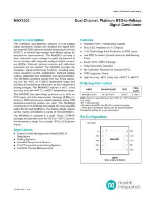
  • 1. General Description The MAX6603 dual-channel, platinum RTD-to-voltage signal conditioner excites and amplifies the signal from two external 200Ω platinum-resistive temperature devices (Pt RTD) to achieve high-voltage, level-filtered signals for temperature measurements. The MAX6603 provides a direct ratiometric output voltage to simplify the interface to microcontrollers with integrated analog-to-digital convert- ers (ADCs). External precision resistors and calibration processes are not needed. The MAX6603 provides the necessary signal-conditioning functions, including ratio- metric excitation current, amplification, buffered voltage outputs, diagnostic fault detections, and input protection. The MAX6603 amplifies signals from two RTDs operat- ing over the -40°C to +1000°C temperature range and provides the temperature information as two independent analog voltages. The MAX6603 features a ±6°C (max) accuracy over the +400°C to +600°C temperature range. The MAX6603 has overvoltage protection up to +16V on RTD inputs, and ±5kV electrostatic discharge (ESD) pro- tection at RTD input pins for reliable operation where RTD temperature-sensing probes are used. The MAX6603 monitors the RTD for faults and asserts the respective DG output low for fault conditions. The analog voltage outputs can be readily connected to a variety of microcontrollers. The MAX6603 is available in a small, 10-pin TDFN-EP package and operates over the -40°C to +125°C automo- tive temperature range from a single +3V to +5.5V power supply. Applications ●● Engine Control Management to Meet EURO IV Regulations ●● Braking Systems ●● Industrial Temperature Sensors ●● Food Transportation Monitoring Systems ●● Industrial Process Measurements Features ●● Amplifies Pt RTD Temperature Signals ●● ±5kV ESD Protection on RTD Inputs ●● +16V Overvoltage Fault Protection on RTD Inputs ●● Low RTD Excitation Current Minimizes Self-Heating Errors ●● Small, 10-Pin TDFN Package ●● Fully Ratiometric Operation ●● No Calibration Required for Standard RTDs ●● RTD Diagnostic Check ●● High Accuracy: ±6°C (max) from +400°C to +600°C 19-3975; Rev 1; 4/14 Note: Device is specified over the -40°C to +125°C tempera- ture range. *EP = Exposed pad. +Denotes a lead(Pb)-free/RoHS-compliant package. **Other base resistance values can be accommodated. Contact the factory for more information. PART PIN-PACKAGE RTD PKG CODE MAX6603ATB+ 10 TDFN-EP* 200Ω** T1033-1 1 3 4 10+ 8 7 OUT1 VCC RS2+ RS1+ MAX6603 2 9 OUT2RS2- 5 6 GNDRS1- TDFN 3mm x 3mm x 0.8mm TOP VIEW DG2 DG1 MAX6603 Dual-Channel, Platinum RTD-to-Voltage Signal Conditioner Pin Configuration Ordering Information EVALUATION KIT AVAILABLE
  • 2. (All voltages referenced to GND, unless otherwise noted.) VCC........................................................................-0.3V to +6.0V RS1+, RS1-, RS2+, RS2-....................................-0.3V to +18.0V OUT1, OUT2, DG1, DG2.......................... -0.3V to (VCC + 0.3V) Continuous Power Dissipation (TA = +70°C) 10-Pin TDFN Single-Layer Board (derate 18.5 mW/°C above +70°C).........................1481.5mW 10-Pin TDFN Multilayer Board (derate 24.4 mW/°C above +70°C).........................1951.2mW ESD Protection (OUT1, OUT2, DG1, DG2, Human Body Model).......................................................>±2kV ESD Protection (RS1+, RS2+, RS1-, RS2-, VCC, GND, Human Body Model)...................................>±5kV Operating Temperature Range.......................... -40°C to +125°C Junction Temperature.......................................................+150°C Storage Temperature Range............................. -65°C to +150°C Lead Temperature (soldering, 10s)..................................+300°C (VCC = 3.0V to 5.5V, resistor connected between RS1+ and RS1- = 560Ω, resistor connected between RS2+ and RS2- = 560Ω, TA = -40°C to +125°C, unless otherwise noted. Typical values are at VCC = 5.0V, RL = 47kΩ between OUT_ and GND, TA = +25°C.) (Note 1) PARAMETER SYMBOL CONDITIONS MIN TYP MAX UNITS Supply Voltage VCC 3.0 5.5 V Input Over Voltage VRS RS1+, RS1-, RS2+, RS2- 16 V Supply Current ICC 3.9 5.5 mASink current during overvoltage fault VRS1+ = VRS1 - = VRS2+ = VRS2- = +16V 36.2 47.1 CURRENT SOURCES Excitation Current IEXC (Note 2) 0.58 1.0 1.12 mA Excitation-Current Temperature Coefficient TCIEXC (Note 2) -7 ppm/°C Minimum RS_- Voltage VRS_- 3.4 V Maximum RS_+ Voltage VRS_+ 4.0 V Supply Ratiometric IRATIO VCC = +3V to +5.5V 0.2 mA/V MAXIMUM TEMPERATURE ERROR (Note 3) RTD +400°C to +600°C, VCC = 5.0V ±6 °C -40°C to +400°C, VCC = 5.0V ±8 +600°C to +1000°C, VCC = 5.0V ±12 +400°C to +600°C, VCC = 3.0V ±10 -40°C to +400°C, VCC = 3.0V ±13.3 +600°C to +1000°C, VCC = 3.0V ±20 MAX6603 Dual-Channel, Platinum RTD-to-Voltage Signal Conditioner www.maximintegrated.com Maxim Integrated │  2 Absolute Maximum Ratings Stresses beyond those listed under “Absolute Maximum Ratings” may cause permanent damage to the device. These are stress ratings only, and functional operation of the device at these or any other conditions beyond those indicated in the operational sections of the specifications is not implied. Exposure to absolute maximum rating conditions for extended periods may affect device reliability. Electrical Characteristics
  • 3. (VCC = 3.0V to 5.5V, resistor connected between RS1+ and RS1- = 560Ω, resistor connected between RS2+ and RS2- = 560Ω, TA = -40°C to +125°C, unless otherwise noted. Typical values are at VCC = 5.0V, RL = 47kΩ between OUT_ and GND, TA = +25°C.) (Note 1) Note 1: All parameters are tested at TA = +25°C. Specifications over temperature are guaranteed by design. Note 2: RTD resistance range is 150Ω to 900Ω for constant excitation current. Note 3: A typical 200Ω RTD: R(T) = RO[1 + AT + BT2] is referenced for probe temperature-probe resistance relation. The param- eters in this section are not tested and are for reference only. Note 4: RTD resistance is tested only at RRTD = 200Ω, 560Ω, 845Ω. The range is guaranteed by design. Note 5: Parameters are tested in special test mode. PARAMETER SYMBOL CONDITIONS MIN TYP MAX UNITS MAXIMUM INPUT RESISTANCE-TO-OUTPUT VOLTAGE ERROR RTD (Note 4) 494Ω to 627Ω, VCC = 5.0V 19 mV 200Ω to 494Ω, VCC = 5.0V 27 627Ω to 866Ω, VCC = 5.0V 33 494Ω to 627Ω, VCC = 3.0V 19 200Ω to 494Ω, VCC = 3.0V 27 627Ω to 866Ω, VCC = 3.0V 33 ANALOG OUTPUTS (OUT1, OUT2) Output-Voltage Low (Max) VOL RL = 47kΩ between OUT_ and VCC (Note 5) 0.1 V Output-Voltage High (Min) VOH RL = 47kΩ between OUT_ and GND (Note 5) VCC - 0.1 V Short-Circuit Current ISC VOUT = VCC 22 mA VOUT = GND 12 mA Maximum Capacitive Load CL 500 pF Minimum Resistive Load RL Between OUT_ and GND 20 kΩ DIAGNOSTIC OUTPUTS (DG1, DG2) Output-Voltage Low VOL ISOURCE = 1mA 0.2 V Output-Voltage High VOH ISINK = 1mA VCC - 0.2 V Minimum Resistance for RS+, RS - Open RRS - OPEN 8000 Ω Maximum Resistance for RS+, RS - Short RRS - SHORT 60 Ω MAX6603 Dual-Channel, Platinum RTD-to-Voltage Signal Conditioner www.maximintegrated.com Maxim Integrated │  3 Electrical Characteristics (continued)
  • 4. (VCC = 5.0V, TA = +25°C, unless otherwise noted.) -20 10 0 -10 20 -40 -10 20 50 80 110 OUTPUT-VOLTAGE DRIFT vs. TEMPERATURE MAX6603toc02 TEMPERATURE (°C) OUTPUT-VOLTAGEDRIFT(mV) POWER-SUPPLY REJECTION RATIO vs. FREQUENCY MAX6603toc03 FREQUENCY (kHz) PSRR(dB) 100.0010.001.000.10 -90 -80 -70 -60 -50 -40 -30 -20 -10 0 -100 0.01 1000.00 0 1 3 2 4 5 OUTPUT VOLTAGE vs. RTD RESISTANCE MAX6603toc04 RTD RESISTANCE (Ω) OUTPUTVOLTAGE(V) 100 500300 700 900 TA = 25°C 2.0 2.6 2.3 3.2 2.9 3.5 3.8 3.0 5.5 SUPPLY CURRENT vs. SUPPLY VOLTAGE MAX6603toc01 SUPPLY VOLTAGE (V) SUPPLYCURRENT(mA) 4.03.5 4.5 5.0 TA = -40°C TA = 0°C TA = +125°C TA = +85°C TA = +25°C MAX6603 Dual-Channel, Platinum RTD-to-Voltage Signal Conditioner Maxim Integrated │  4www.maximintegrated.com Typical Operating Characteristics
  • 5. Detailed Description The MAX6603 converts a Deutsche Institute for Normung (DIN) standard 200Ω Pt RTD to a high-level analog volt- age without the need for external trims or precise discrete components. The Pt RTD resistance conveys tempera- ture information approximated by the Callendar-Van Dusen equation and is represented in Figure 1: R(T) = RO[1 + AT + BT2+ CT3] where: R(T) = Resistance of Pt RTD at temperature (T) R0 = Base resistance in ohms at 0°C T = Temperature in °C A = 3.9083 E-3 °C-1 (alpha coefficient 1) B = -5.7750 E-7 °C-2 (alpha coefficient 2) C = 0 (approximation for temperatures > 0°C) (Alpha coefficients can vary depending on standards.) The MAX6603 applies a constant excitation current of 1mA (typ) through the Pt RTD, generating a voltage drop that is amplified and results in a high-level output voltage. The excitation current (IEXC) typically varies ratiometrically by 0.2mA/V (typ) with respect to VCC, and therefore, the amplified signal is ratiometric to the power supply. The voltage amplification from input to output is 5 (typ). The output voltage is applied to a ratiometric ADC to produce a digital value independent of supply voltage. For ADCs that use VCC as their reference voltage, sudden changes in the supply voltage do not affect the microcontroller’s reading of the temperature. Ratiometricity simplifies the connec- tion to most microcontrollers that incorporate an ADC and PIN NAME FUNCTION 1 VCC Power-Supply Input. Bypass to GND with a 0.1µF capacitor as close to VCC as possible. 2 RS2- Sense Resistor 2 Negative Input 3 RS2+ Sense Resistor 2 Positive Input 4 RS1+ Sense Resistor 1 Positive Input 5 RS1- Sense Resistor 1 Negative Input 6 GND Ground 7 DG1 Diagnostic Output Signal 1. DG1 asserts low upon fault detection. 8 OUT1 Output Analog Voltage 1. OUT1 is high impedance upon DG1 assertion. 9 OUT2 Output Analog Voltage 2. OUT2 is high impedance upon DG2 assertion. 10 DG2 Diagnostic Output Signal 2. DG2 asserts low upon fault detection. — EP Exposed Pad. Connect to GND. MAX6603 RS1+ RS1- OUT1AMP FAULT DETECT DG1 HI-V DETECT IEXCESD CLAMP ESD CLAMP VCC RSRC RS2+ RS2- OUT2AMP FAULT DETECT DG2 HI-V DETECT IEXCESD CLAMP ESD CLAMP VCC RSRC VCC GND MAX6603 Dual-Channel, Platinum RTD-to-Voltage Signal Conditioner www.maximintegrated.com Maxim Integrated │  5 Pin Description Functional Block Diagram
  • 6. enables a low-cost, low-complexity solution. Ratiometricity is an important consideration for battery-operated instruments and some industrial applications. Temperature Information The MAX6603 measures the resistance between the RTD and translates that into a high-level output voltage. The resistance range of the MAX6603 is between 150Ω and 900W, covering a -40°C to +1000°C temperature range. When R(T) goes too low or too high, a fault condition is asserted and the respective DG_ goes low. Output Voltage The following equation describes the output voltage: CC OUT V R(T) V 1000 × = where: VCC = supply voltage R(T) = RTD resistance given by Callendar- Van Dusen equation. Using Other Pt RTDs The MAX6603 is designed for a 200Ω Pt RTD, but the device can work with any RTD as long as the resistance is in the 150Ω to 900Ω range. A 500Ω Pt RTD can be used for temperatures up to +208°C because that temperature results in R(T) = 900Ω. Input Overvoltage Protection to +16V The input pins RS1+, RS1-, RS2+, and RS2- protect the MAX6603 from overvoltage conditions up to +16V without damaging the device. Diagnostic Outputs (DG1, DG2) The MAX6603 continuously monitors the excitation cur- rent to the RTD, the resultant voltage drop, and voltage levels of the inputs to detect fault conditions. Any fault condition causes the respective DG output to assert low. Fault conditions occur for RTD open circuits; RTD short circuits; and RS1+, RS1-, RS2+, and RS2- short to ground or supply. If any fault is detected, the respec- tive DG output asserts low. OUT1 and OUT2 are high impedance on assertion of DG1 and DG2, respectively. An example circuit showing potential fault conditions is shown in Figure 2. Applications Information Ratiometric Output Coupled to a Microcontroller The circuit of Figure 3 shows the MAX6603 connected to the microcontroller using VCC as the ADC reference volt- age. The output is ratiometric to VCC, and temperature measurements are independent of the supply voltage. Chip Information PROCESS: BiCMOS Figure 1. Typical 200Ω Pt RTD Representation by the Simplified Callender-Van Dusen Equation 0 300 200 100 400 500 600 700 800 900 1000 0 400200 600 800 1000 200Ω Pt RTD TEMPERATURE (°C) RESISTANCE(Ω) MAX6603 Dual-Channel, Platinum RTD-to-Voltage Signal Conditioner www.maximintegrated.com Maxim Integrated │  6
  • 7. Figure 2. The various fault conditions that cause the diagnostic output to assert low are shown for a single channel. MAX6603 RS1+ RS1- OUT1 AMP FAULT DETECT DG1 HI-V DETECT IEXCESD CLAMP ESD CLAMP VCC RSRC RS2+ RS2- OUT2 AMP FAULT DETECT DG2 HI-V DETECT IEXCESD CLAMP ESD CLAMP VCC RSRC VCC GND 0.1µF 0.1µF OUT1 ADC2 INPUT2 ADC1 INPUT1 +5V VCCADC-REF 5kV ESD SHORT TOGETHEROPEN OPEN SHORT TO BAT (16V) SHORT TO BAT (16V) SHORT TO GND SHORT TO GND RTD SENSOR CHASSIS GND MICROCONTROLLER MAX6603 Dual-Channel, Platinum RTD-to-Voltage Signal Conditioner www.maximintegrated.com Maxim Integrated │  7
  • 8. Figure 3. A Typical Application Circuit with Ratiometric Output Coupled to Ratiometric Microcontroller ADC PACKAGE TYPE PACKAGE CODE OUTLINE NO. LAND PATTERN NO. 10 TDFN T1033+1 21-0137 90-0003 MAX6603 RS1+ RS1- RS2+ RS2- OUT1 AMP FAULT DETECT DG1 HI-V DETECT IEXCESD CLAMP ESD CLAMP VCC RSRC OUT2 AMP FAULT DETECT DG2 HI-V DETECT IEXCESD CLAMP ESD CLAMP VCC RSRC VCC GND 0.1µF 0.1µF OUT1 ADC2 INPUT2 ADC1 INPUT1 +5V ADC-REF MICROCONTROLLER Pt RTD PROBE Pt RTD PROBE CONNECTOR CONNECTOR MAX6603 Dual-Channel, Platinum RTD-to-Voltage Signal Conditioner www.maximintegrated.com Maxim Integrated │  8 Package Information For the latest package outline information and land patterns (footprints), go to www.maximintegrated.com/packages. Note that a “+”, “#”, or “-” in the package code indicates RoHS status only. Package drawings may show a different suffix character, but the drawing pertains to the package regardless of RoHS status.
  • 9. REVISION NUMBER REVISION DATE DESCRIPTION PAGES CHANGED 0 4/06 Initial release — 1 4/14 No /V OPNs; removed Automotive reference from Applications section 1 Maxim Integrated cannot assume responsibility for use of any circuitry other than circuitry entirely embodied in a Maxim Integrated product. No circuit patent licenses are implied. Maxim Integrated reserves the right to change the circuitry and specifications without notice at any time. The parametric values (min and max limits) shown in the Electrical Characteristics table are guaranteed. Other parametric values quoted in this data sheet are provided for guidance. Maxim Integrated and the Maxim Integrated logo are trademarks of Maxim Integrated Products, Inc. MAX6603 Dual-Channel, Platinum RTD-to-Voltage Signal Conditioner © 2014 Maxim Integrated Products, Inc. │  9 Revision History For pricing, delivery, and ordering information, please contact Maxim Direct at 1-888-629-4642, or visit Maxim Integrated’s website at www.maximintegrated.com.