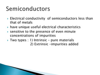
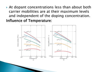
SlideShare a Scribd company logo
MATERIAL SCIENCE ASSIGNMENT
NIT CALICUT
SUBMITTED BY:
T.VINAYASREE
MOOLA NIHARIKA
NAKA PRIYANKA
HARISH.M
MANOJ MADHAV
MOHAMMED ARSHAK
MOHAMED HARSHID
 Ohm’s law relates the current I to the applied voltage V as follows:
where R - resistance of the material.
Units: V : volts (j/c)
I : amperes (c/s)
R : ohms (V/A )
 The resistivity ‘ρ’ is independent of specimen geometry.
where
l : distance between 2 points at which voltage is measured
A : cross sectional area perpendicular to the direction of
the current.
units : ρ ohm meter (Ω-m)
It is defined as the reciprocal of resistivity
 It indicates the case with which a material is capable of conducting
an electric current.
units : σ ( ohm meter (1 ̸Ωm ) )
 ohm’s law can be expressed as
where J – current density [I/A]
E – Electric field density ( v/l )
 solid materials are classified according to ease with whivh they conduct
electric current . They are classified as
1) conductors : conductivity order
2) insulators
3) semi conductors
 An electric current results from the motion of electrically charged
particles in response to forces that act on them from an externally
applied electric field.
 Within most solid materials a current arises from the flow of
electrons, which is termed electronic conduction.
 For ionic materials a net motion of charged ions is possible that
produces a current; such is termed ionic conduction.
 ENERGY BAND STRUCTURES IN SOLIDS:
 In all conductors, semiconductors, and many insulating materials,
only electronic.
 Conduction exists which is strongly dependent on number of
electros available to participate in the conduction process.
 These electrons are related to the arrangement of electron states or
levels.
 For each individual atom there exist discrete energy levels that may
be occupied by electrons, arranged into shells and subshells.
 Shells are designated by integers (1, 2, 3, etc.), and for each
subshells represented by letters (s, p, d, and f ) there exists one,
three, five, seven states respectively.
 Pauli exclusion principle states that the electrons fill in the states
with lower energy with two electrons of opposite spins.
 A solid may be thought of as consisting of a large number of atoms(say
N) that are brought together and bounded to form the ordered atomic
arrangement.
 Each atom has atomic levels that split into a series of closely spaced
electrons in solid to form electron energy band.
 The extent of splitting depends on interatomic separation.
 Within each band, the energy states are discrete, yet the difference
between adjacent states is exceedingly small.
 The number of states within each band will equal the total of all states
contributed by the N atoms.
 each energy state accommodate two electrons, which must have
oppositely directed spins.
 Four different types of band structures are possible at 0 K.
a. In the first one outermost band is only partially filled with
electrons.The energy corresponding to the highest filled state at 0
K is called the Fermi energy Ef.
b. For the second band structure, there is an overlap of an empty
band and a filled band. Eg:Magnesium.
c. The final two band structures are similar; one band (the valence
band) that is completely filled with electrons is separated from an
empty conduction band, and an energy band gap lies between
them.
 For the insulators band gap is relatively wide whereas for
semiconductors it is narrow.
 The energy corresponding to the highest filled state at 0k is
called Fermi energy.
 Electrons with energies greater than the Fermi energy acted on
them can be accelerated in the presence of an electric field.
 The electrons that participate in the conduction process are
known as free electrons.
 Electrical conductivity is a direct function of the numbers of
free electrons and holes.
For an electron to become free, it must be excited or
promoted into one of the empty and available energy
states above Fermi energy.
The energy band gap for metals is almost zero for
metals,so they are very good conductors.
 For insulators and semiconductors, empty states adjacent to the top of the
filled valence band are not available.
 To become free, electrons must be promoted across the energy band gap.
 The number of electrons excited thermally (by heat energy) into the
conduction band depends on the energy band gap width as well as
temperature.
 Larger the band gap, the lower is the electrical conductivity at a given
temperature.
 For insulators the width of the band gap is narrow whereas for insulators, it
is relatively wide.
 Increasing the temperature of either a semiconductor or an insulator results
in an increase in the thermal energy that is available for electron excitation.
So,conductivity increases.
 For electrically insulating materials, interatomic
bonding is ionic or strongly covalent.
 Thus, the valence electrons are tightly bound to or
shared with the individual atoms.
 The bonding in semiconductors is covalent and
relatively weak, which means that the valence
electrons are not as strongly bound to the atoms.
 So, these electrons are more easily removed by
thermal excitation than they are for insulators.
 When an electric field is applied, a force is brought to bear on
the free electrons;so, they all experience an acceleration in a
direction opposite to that of the field, by virtue of their
negative charge.
 All the free electrons accelerate as long as the electric field is
applied, which will give rise to an electric current that
continuously increases with time.
 Current reaches a constant value the instant that a field is
applied, indicating that there exist “frictional forces,” that
counter this acceleration from the external field.
.
 These frictional forces result from the scattering of electrons by
imperfections in the crystal lattice, including impurity atoms vacancies,
interstitial atoms, dislocations, and even the thermal vibrations of the atoms
themselves.
 Each scattering event causes an electron to lose kinetic energy and to
change it direction of motion.
 The drift velocity represents the average electron velocity in
the direction of the force imposed by the applied field. It is
directly proportional to the electric field as
 The constant of proportionality µe is called the electron
mobility, which is an indication of the frequency of scattering
events.
 Units are square meters per volt-second(m2/V-s).
 The conductivity of most materials is
expressed as
 where ,
 n is the number of free or conducting electrons per unit
volume (e.g., per cubic meter), and |e| is the absolute
magnitude of the electrical charge on an electron .
 Thus, the electrical conductivity is proportional to both
the number of free electrons and the electron mobility.
 Most metals are extremely good conductors of electricity.
 Metals have high conductivities because of the large numbers
of free electrons that have been excited into empty states
above the Fermi energy.
 Crystalline defects serve as scattering centers for conduction
electrons in metals, increasing their number raises the
resistivity (or lowers the conductivity).
 The concentration of these imperfections depends on
temperature, composition,and the degree of cold work of a
metal specimen.
 The total resistivity of a metal is the sum of the contributions
from thermal vibrations, Impurities, and plastic deformation.
 Where ρt,ρi,ρd represent the individual thermal, impurity, and
deformation resistivity contributions, respectively.
 The above is sometimes known as Mat-thiessen’s rule.
 For the pure metal and all the copper–nickel alloys, the
resistivity rises linearly with temperature:
 where ρo and a are constants for each particular metal.This
dependence of the thermal resistivity component on
temperature is due to the increase with temperature in thermal
vibrations and other lattice irregularities (e.g., vacancies),
which serve as electron-scattering centers.
 For additions of a single impurity that forms a solid
solution, the impurity resistivity ρi is related to the
impurity concentration ci in terms of the atom fraction
(at%100) as follows:
 ρi =Aci(1-ci)
 A is a composition-independent constant that is a function of
both the impurity and host metals.
 For a two-phase alloy consisting of and phases, a rule-of-
mixtures expression is used to approximate the resistivity as:
 where the V’s and ’s represent volume fractions and individual
resistivities for the respective phases.
..
 Copper render it the most widely used metallic conductor.
 Oxygen-free high-conductivity (OFHC) copper, having
extremely low oxygen and other impurity contents, is
produced for many electrical applications.
 Both solid-solution alloying and cold working improve
strength at the expense of conductivity.
 For some applications, such as furnace heating elements
materials must have not only a high resistivity, but also a
resistance to oxidation at elevated temperatures and,a high
melting temperature.
 Nichrome, a nickel–chromium alloy, is commonly employed
in heating elements
 Electrical conductivity of semiconductors less than
that of metals
 have unique useful electrical characteristics
 sensitive to the presence of even minute
concentrations of impurities
 Two types : 1) Intrinsic – pure materials
2) Extrinsic –impurities added
 band structure
 relatively narrow forbidden band
gap (<2 eV)
 Eg : Si (1.1eV) and Ge(0.7eV)
 Also compounds composed of
Groups IIIA and VA – GaAs, In Sb
Groups IIB and VIA- Cd S, Zn Te
 In above compounds ,
->dissimiar electronegativities
-> atomic bonding becomes more ionic
-> band gap energy increases—more
insulative
 a vacant electron state in the VB created because of
e- from VB excited to CB
 Treating a missing electron from the valence band
as a positively charged particle called
a hole.
 Charge of hole= +1.6x10^-19 C
 In the presence of an electric field, excited
electrons and holes move in opposite directions
 Two types of charge
carrier (free electrons
and holes)
 p is the number of
holes per cubic meter
 µh is the hole mobility
 ni is known as the
intrinsic carrier
concentration
 impurity concentration determines the
electrical behavior of semiconductors
 One atom in 10^12 is sufficient to render
silicon extrinsic at room temperature.
 Types : 1) n-type
2) p-type
 Si has 4 e-s : covalent bonded with other
adjacent atoms
 If we add a Grp VA impurity , 4e-s form
bonds , there will be 1 e- free .
 It is free e- / conducting e-
 For these free e-s , energy state is in
forbidden band gap just below CB
 If energy is given,e- get excited to CB
 Hence this type impurity is termed a ‘donor’
 No hole in VB
 At room temp, we can easily excite
large no. of e-s from donor states
 No.of e-s in CB >>no.of holes in
VB
 This type material is n-type
extrinsic semiconductors
 e- are majority carriers
 Holes are minority charge carriers
 n-type : Fermi level shifted
upward in band gap
 If we add a Group IIIA such as Al, Ga, B three electrons form bonds.
 One covalent bond is deficient in electrons. This is called Hole. It
participates in conduction process.
 Impurity atom introduces energy close to the top of valence band in
band gap.
 No free electrons are created either in valence band or conduction band.
 This type of impurity is called acceptor.
 For p>>n material is called P type(positively charged)
 Holes are majority carries ,electronns are minority.
 For P type, fermi level with bond gap near to the acceptor level.
 Extrinsic semiconductors (both n- and p-type) Controlled
concentrations of specific donors or acceptors are then intentionally
added.
 This alloying process in
 semiconducting materials is termed doping.
 At relatively high room-temperature electrical conductivities are
obtained in extrinsic semiconductors
 Figure,plots the logarithm of the intrinsic carrier
concentration versus temperature
for both silicon and germanium.
 The concentrations of electrons and holes increase
with temperature because, with rising temperature
 At all temperatures, carrier concentration in Ge is
greater than for Si . This effect is due to germanium’s
smaller band gap thus, for Ge, at any given
temperature more electrons will be excited across its
band gap.
 The conductivity (or resistivity) of a semiconducting material, in addition
to being dependent on electron and/or hole concentrations, is also a
function of the charge carriers’ mobilities.
Influence of Dopant Content:
 At dopant concentrations less than about both
carrier mobilities are at their maximum levels
and independent of the doping concentration.
Influence of Temperature:
 The temperature dependences of electron and
hole mobilities for silicon are presented in
above figures.
 These plots, note that, for dopant
concentrations of 10−24
𝑚−3
and below, both
electron and hole mobilities decrease in
magnitude with rising temperature.
Material science  metals, bnads etc.,

More Related Content

What's hot

Chapter 4 Mechanical Engineering Materials 22343
Chapter 4 Mechanical Engineering Materials 22343 Chapter 4 Mechanical Engineering Materials 22343
Chapter 4 Mechanical Engineering Materials 22343
Sandip Polytechnic,Nashik
 
Band alignment JC talk
Band alignment JC talkBand alignment JC talk
Band alignment JC talk
Suzanne Wallace
 
Chapter 9 Electrical Properties
Chapter 9 Electrical PropertiesChapter 9 Electrical Properties
Chapter 9 Electrical Properties
Pem(ເປ່ມ) PHAKVISETH
 
Ferrous and non ferrous alloys by Hari Prasad
Ferrous and non ferrous alloys by Hari PrasadFerrous and non ferrous alloys by Hari Prasad
Ferrous and non ferrous alloys by Hari Prasad
Sachin Hariprasad
 
Ultrasonic machining
Ultrasonic machiningUltrasonic machining
Ultrasonic machining
Parth Date
 
Super lattice and quantum well
Super lattice and quantum wellSuper lattice and quantum well
Super lattice and quantum well
MUHAMMAD AADIL
 
Inclusion control for clean steel
Inclusion control for clean steelInclusion control for clean steel
Inclusion control for clean steelSANTOSH KUMAR
 
magnetic materials (160760109010)
  magnetic materials (160760109010)  magnetic materials (160760109010)
magnetic materials (160760109010)
Ronak Dhola
 
ELECTROCHEMICAL MACHINING - NON TRADITIONAL MACHINING
ELECTROCHEMICAL MACHINING - NON TRADITIONAL MACHININGELECTROCHEMICAL MACHINING - NON TRADITIONAL MACHINING
ELECTROCHEMICAL MACHINING - NON TRADITIONAL MACHINING
Sajal Tiwari
 
SCHOTTKY AND VACANCY DEFECT BY SMITA
SCHOTTKY AND VACANCY DEFECT BY SMITASCHOTTKY AND VACANCY DEFECT BY SMITA
SCHOTTKY AND VACANCY DEFECT BY SMITA
sharmeenkhan15
 
Properties of optical materials
Properties of optical materialsProperties of optical materials
Properties of optical materials
SAAD ARIF
 
Corrosion and degradation of materials
Corrosion and degradation of materialsCorrosion and degradation of materials
Corrosion and degradation of materialsGhassan Alshahiri
 
Semiconductor theory
Semiconductor theorySemiconductor theory
Chapter 2 Mechanical Engineering Materials (22343)
Chapter 2 Mechanical Engineering Materials (22343) Chapter 2 Mechanical Engineering Materials (22343)
Chapter 2 Mechanical Engineering Materials (22343)
Sandip Polytechnic,Nashik
 
Dr.R.Narayanasamy - Super Plasticity
Dr.R.Narayanasamy - Super PlasticityDr.R.Narayanasamy - Super Plasticity
Dr.R.Narayanasamy - Super Plasticity
Dr.Ramaswamy Narayanasamy
 
Transformer Construction And Principle | Electronical Engineering
Transformer Construction And Principle | Electronical EngineeringTransformer Construction And Principle | Electronical Engineering
Transformer Construction And Principle | Electronical Engineering
Transweb Global Inc
 
semiconductor physics
semiconductor physics semiconductor physics
semiconductor physics ruwaghmare
 
Cast iron
Cast ironCast iron

What's hot (20)

Chapter 4 Mechanical Engineering Materials 22343
Chapter 4 Mechanical Engineering Materials 22343 Chapter 4 Mechanical Engineering Materials 22343
Chapter 4 Mechanical Engineering Materials 22343
 
Iron
IronIron
Iron
 
Band alignment JC talk
Band alignment JC talkBand alignment JC talk
Band alignment JC talk
 
Chapter 9 Electrical Properties
Chapter 9 Electrical PropertiesChapter 9 Electrical Properties
Chapter 9 Electrical Properties
 
Ferrous and non ferrous alloys by Hari Prasad
Ferrous and non ferrous alloys by Hari PrasadFerrous and non ferrous alloys by Hari Prasad
Ferrous and non ferrous alloys by Hari Prasad
 
Ultrasonic machining
Ultrasonic machiningUltrasonic machining
Ultrasonic machining
 
Super lattice and quantum well
Super lattice and quantum wellSuper lattice and quantum well
Super lattice and quantum well
 
Inclusion control for clean steel
Inclusion control for clean steelInclusion control for clean steel
Inclusion control for clean steel
 
magnetic materials (160760109010)
  magnetic materials (160760109010)  magnetic materials (160760109010)
magnetic materials (160760109010)
 
ELECTROCHEMICAL MACHINING - NON TRADITIONAL MACHINING
ELECTROCHEMICAL MACHINING - NON TRADITIONAL MACHININGELECTROCHEMICAL MACHINING - NON TRADITIONAL MACHINING
ELECTROCHEMICAL MACHINING - NON TRADITIONAL MACHINING
 
SCHOTTKY AND VACANCY DEFECT BY SMITA
SCHOTTKY AND VACANCY DEFECT BY SMITASCHOTTKY AND VACANCY DEFECT BY SMITA
SCHOTTKY AND VACANCY DEFECT BY SMITA
 
Properties of optical materials
Properties of optical materialsProperties of optical materials
Properties of optical materials
 
Corrosion and degradation of materials
Corrosion and degradation of materialsCorrosion and degradation of materials
Corrosion and degradation of materials
 
Dual phase steels
Dual phase steelsDual phase steels
Dual phase steels
 
Semiconductor theory
Semiconductor theorySemiconductor theory
Semiconductor theory
 
Chapter 2 Mechanical Engineering Materials (22343)
Chapter 2 Mechanical Engineering Materials (22343) Chapter 2 Mechanical Engineering Materials (22343)
Chapter 2 Mechanical Engineering Materials (22343)
 
Dr.R.Narayanasamy - Super Plasticity
Dr.R.Narayanasamy - Super PlasticityDr.R.Narayanasamy - Super Plasticity
Dr.R.Narayanasamy - Super Plasticity
 
Transformer Construction And Principle | Electronical Engineering
Transformer Construction And Principle | Electronical EngineeringTransformer Construction And Principle | Electronical Engineering
Transformer Construction And Principle | Electronical Engineering
 
semiconductor physics
semiconductor physics semiconductor physics
semiconductor physics
 
Cast iron
Cast ironCast iron
Cast iron
 

Viewers also liked

Utm intro to materials science
Utm intro to materials scienceUtm intro to materials science
Utm intro to materials science
mohamednubli
 
Metallic conductor
Metallic conductorMetallic conductor
Metallic conductor
Ahmed_Salih
 
Engineering physics 4(Thermal conductivity)
Engineering physics 4(Thermal conductivity)Engineering physics 4(Thermal conductivity)
Engineering physics 4(Thermal conductivity)
Nexus
 
Superconductivity of Materials (student preso)
Superconductivity of Materials (student preso)Superconductivity of Materials (student preso)
Superconductivity of Materials (student preso)
Roppon Picha
 
Semiconductors
SemiconductorsSemiconductors
Semiconductors
Datha Prasada Rao Vanam
 
4.electrical resistivity of ferromagnetic nickel
4.electrical resistivity of ferromagnetic nickel4.electrical resistivity of ferromagnetic nickel
4.electrical resistivity of ferromagnetic nickel
Narayan Behera
 
Resistivity
ResistivityResistivity
Presentation laser
Presentation  laserPresentation  laser
Presentation laser
Dr. M. K. Deore
 
Solar pumped Laser
Solar pumped LaserSolar pumped Laser
Solar pumped Laser
ajay singh
 
Resistivity
ResistivityResistivity
Ceramic materials 1
Ceramic materials  1Ceramic materials  1
Ceramic materials 1
Dr. M. K. Deore
 
Lecture 1 introduction
Lecture 1 introductionLecture 1 introduction
Lecture 1 introductionAnnalyn Soria
 
Pulsed nd yag laser welding
Pulsed nd yag laser weldingPulsed nd yag laser welding
Pulsed nd yag laser weldingVardaan Sharma
 
project report on REMOTE SENSING THERMOMETER
project report on REMOTE SENSING THERMOMETERproject report on REMOTE SENSING THERMOMETER
project report on REMOTE SENSING THERMOMETER
dreamervikas
 
Fayza ceramics
Fayza ceramicsFayza ceramics
Fayza ceramics
fayza123
 
Material Science and Metallurgy
Material Science and MetallurgyMaterial Science and Metallurgy
Material Science and Metallurgy
taruian
 
Design and development of solar pumped Nd:YAG Laser
Design and development of solar pumped Nd:YAG LaserDesign and development of solar pumped Nd:YAG Laser
Design and development of solar pumped Nd:YAG Laser
ajay singh
 
Insulating materials- electrial
Insulating materials- electrialInsulating materials- electrial
Insulating materials- electrial
SSGMCE SHEGAON
 

Viewers also liked (20)

Utm intro to materials science
Utm intro to materials scienceUtm intro to materials science
Utm intro to materials science
 
Metallic conductor
Metallic conductorMetallic conductor
Metallic conductor
 
Engineering physics 4(Thermal conductivity)
Engineering physics 4(Thermal conductivity)Engineering physics 4(Thermal conductivity)
Engineering physics 4(Thermal conductivity)
 
Superconductivity of Materials (student preso)
Superconductivity of Materials (student preso)Superconductivity of Materials (student preso)
Superconductivity of Materials (student preso)
 
Semiconductors
SemiconductorsSemiconductors
Semiconductors
 
4.electrical resistivity of ferromagnetic nickel
4.electrical resistivity of ferromagnetic nickel4.electrical resistivity of ferromagnetic nickel
4.electrical resistivity of ferromagnetic nickel
 
Lecture 3 oms
Lecture 3 omsLecture 3 oms
Lecture 3 oms
 
Resistivity
ResistivityResistivity
Resistivity
 
Lecture 14
Lecture 14Lecture 14
Lecture 14
 
Presentation laser
Presentation  laserPresentation  laser
Presentation laser
 
Solar pumped Laser
Solar pumped LaserSolar pumped Laser
Solar pumped Laser
 
Resistivity
ResistivityResistivity
Resistivity
 
Ceramic materials 1
Ceramic materials  1Ceramic materials  1
Ceramic materials 1
 
Lecture 1 introduction
Lecture 1 introductionLecture 1 introduction
Lecture 1 introduction
 
Pulsed nd yag laser welding
Pulsed nd yag laser weldingPulsed nd yag laser welding
Pulsed nd yag laser welding
 
project report on REMOTE SENSING THERMOMETER
project report on REMOTE SENSING THERMOMETERproject report on REMOTE SENSING THERMOMETER
project report on REMOTE SENSING THERMOMETER
 
Fayza ceramics
Fayza ceramicsFayza ceramics
Fayza ceramics
 
Material Science and Metallurgy
Material Science and MetallurgyMaterial Science and Metallurgy
Material Science and Metallurgy
 
Design and development of solar pumped Nd:YAG Laser
Design and development of solar pumped Nd:YAG LaserDesign and development of solar pumped Nd:YAG Laser
Design and development of solar pumped Nd:YAG Laser
 
Insulating materials- electrial
Insulating materials- electrialInsulating materials- electrial
Insulating materials- electrial
 

Similar to Material science metals, bnads etc.,

Electrical and Magnetic Properties of Materials
Electrical and Magnetic Properties of MaterialsElectrical and Magnetic Properties of Materials
Electrical and Magnetic Properties of Materials
Abeni9
 
u6Lect-1.ppt
u6Lect-1.pptu6Lect-1.ppt
Engineering Physics - II second semester Anna University lecturer notes
Engineering Physics - II second semester Anna University lecturer notesEngineering Physics - II second semester Anna University lecturer notes
Engineering Physics - II second semester Anna University lecturer notes
24x7house
 
Current electricity
Current electricityCurrent electricity
Current electricity
VASUDEV SHRIVASTAVA
 
Semiconductors (rawat d agreatt)
Semiconductors (rawat d agreatt)Semiconductors (rawat d agreatt)
Semiconductors (rawat d agreatt)
Rawat DA Greatt
 
Module 1 Semiconductors (1).pptx
Module 1  Semiconductors (1).pptxModule 1  Semiconductors (1).pptx
Module 1 Semiconductors (1).pptx
PriyaSharma135745
 
Ohms law
Ohms lawOhms law
Ohms law
xastty0501
 
Electricity: Resistance
Electricity: ResistanceElectricity: Resistance
Electricity: Resistance
Pamantasan ng Lungsod ng Maynila
 
Basics in electricity lect 1
Basics in electricity lect 1Basics in electricity lect 1
Basics in electricity lect 1
Dr. Prashant Kaushik
 
Bonding in metals
Bonding in metalsBonding in metals
Bonding in metals
LIFE SCIENCES
 
Engineering physics
Engineering physicsEngineering physics
Engineering physics
Nexus
 
Ph8253 physics for electronics engineering
Ph8253 physics for electronics engineeringPh8253 physics for electronics engineering
Ph8253 physics for electronics engineering
SindiaIsac
 
Semi conductor materials.pptx
Semi conductor materials.pptxSemi conductor materials.pptx
Semi conductor materials.pptx
AliRaZaAnsari13
 
Electric current flow
Electric current flowElectric current flow
Electric current flowEdmund Merren
 
CHEM NOTES Syllbus(20216-23)onwards.docx
CHEM NOTES Syllbus(20216-23)onwards.docxCHEM NOTES Syllbus(20216-23)onwards.docx
CHEM NOTES Syllbus(20216-23)onwards.docx
jyotidighole2
 
Mottphysics 1talk
Mottphysics  1talkMottphysics  1talk
Mottphysics 1talk
ABDERRAHMANE REGGAD
 
хагас дамжуулагчийн физик
хагас дамжуулагчийн физикхагас дамжуулагчийн физик
хагас дамжуулагчийн физикJkl L
 
Bandtheory of solids
Bandtheory of solidsBandtheory of solids
Bandtheory of solids
kveerabhadrarao1
 
Semiconcuctor devices introduction
Semiconcuctor devices  introductionSemiconcuctor devices  introduction
Semiconcuctor devices introduction
RachnaRishi2
 
electricity soham 10th.pptx
electricity soham 10th.pptxelectricity soham 10th.pptx
electricity soham 10th.pptx
JayeshPatil592969
 

Similar to Material science metals, bnads etc., (20)

Electrical and Magnetic Properties of Materials
Electrical and Magnetic Properties of MaterialsElectrical and Magnetic Properties of Materials
Electrical and Magnetic Properties of Materials
 
u6Lect-1.ppt
u6Lect-1.pptu6Lect-1.ppt
u6Lect-1.ppt
 
Engineering Physics - II second semester Anna University lecturer notes
Engineering Physics - II second semester Anna University lecturer notesEngineering Physics - II second semester Anna University lecturer notes
Engineering Physics - II second semester Anna University lecturer notes
 
Current electricity
Current electricityCurrent electricity
Current electricity
 
Semiconductors (rawat d agreatt)
Semiconductors (rawat d agreatt)Semiconductors (rawat d agreatt)
Semiconductors (rawat d agreatt)
 
Module 1 Semiconductors (1).pptx
Module 1  Semiconductors (1).pptxModule 1  Semiconductors (1).pptx
Module 1 Semiconductors (1).pptx
 
Ohms law
Ohms lawOhms law
Ohms law
 
Electricity: Resistance
Electricity: ResistanceElectricity: Resistance
Electricity: Resistance
 
Basics in electricity lect 1
Basics in electricity lect 1Basics in electricity lect 1
Basics in electricity lect 1
 
Bonding in metals
Bonding in metalsBonding in metals
Bonding in metals
 
Engineering physics
Engineering physicsEngineering physics
Engineering physics
 
Ph8253 physics for electronics engineering
Ph8253 physics for electronics engineeringPh8253 physics for electronics engineering
Ph8253 physics for electronics engineering
 
Semi conductor materials.pptx
Semi conductor materials.pptxSemi conductor materials.pptx
Semi conductor materials.pptx
 
Electric current flow
Electric current flowElectric current flow
Electric current flow
 
CHEM NOTES Syllbus(20216-23)onwards.docx
CHEM NOTES Syllbus(20216-23)onwards.docxCHEM NOTES Syllbus(20216-23)onwards.docx
CHEM NOTES Syllbus(20216-23)onwards.docx
 
Mottphysics 1talk
Mottphysics  1talkMottphysics  1talk
Mottphysics 1talk
 
хагас дамжуулагчийн физик
хагас дамжуулагчийн физикхагас дамжуулагчийн физик
хагас дамжуулагчийн физик
 
Bandtheory of solids
Bandtheory of solidsBandtheory of solids
Bandtheory of solids
 
Semiconcuctor devices introduction
Semiconcuctor devices  introductionSemiconcuctor devices  introduction
Semiconcuctor devices introduction
 
electricity soham 10th.pptx
electricity soham 10th.pptxelectricity soham 10th.pptx
electricity soham 10th.pptx
 

Recently uploaded

J.Yang, ICLR 2024, MLILAB, KAIST AI.pdf
J.Yang,  ICLR 2024, MLILAB, KAIST AI.pdfJ.Yang,  ICLR 2024, MLILAB, KAIST AI.pdf
J.Yang, ICLR 2024, MLILAB, KAIST AI.pdf
MLILAB
 
Gen AI Study Jams _ For the GDSC Leads in India.pdf
Gen AI Study Jams _ For the GDSC Leads in India.pdfGen AI Study Jams _ For the GDSC Leads in India.pdf
Gen AI Study Jams _ For the GDSC Leads in India.pdf
gdsczhcet
 
ASME IX(9) 2007 Full Version .pdf
ASME IX(9)  2007 Full Version       .pdfASME IX(9)  2007 Full Version       .pdf
ASME IX(9) 2007 Full Version .pdf
AhmedHussein950959
 
Nuclear Power Economics and Structuring 2024
Nuclear Power Economics and Structuring 2024Nuclear Power Economics and Structuring 2024
Nuclear Power Economics and Structuring 2024
Massimo Talia
 
ethical hacking in wireless-hacking1.ppt
ethical hacking in wireless-hacking1.pptethical hacking in wireless-hacking1.ppt
ethical hacking in wireless-hacking1.ppt
Jayaprasanna4
 
Sachpazis:Terzaghi Bearing Capacity Estimation in simple terms with Calculati...
Sachpazis:Terzaghi Bearing Capacity Estimation in simple terms with Calculati...Sachpazis:Terzaghi Bearing Capacity Estimation in simple terms with Calculati...
Sachpazis:Terzaghi Bearing Capacity Estimation in simple terms with Calculati...
Dr.Costas Sachpazis
 
block diagram and signal flow graph representation
block diagram and signal flow graph representationblock diagram and signal flow graph representation
block diagram and signal flow graph representation
Divya Somashekar
 
ethical hacking-mobile hacking methods.ppt
ethical hacking-mobile hacking methods.pptethical hacking-mobile hacking methods.ppt
ethical hacking-mobile hacking methods.ppt
Jayaprasanna4
 
addressing modes in computer architecture
addressing modes  in computer architectureaddressing modes  in computer architecture
addressing modes in computer architecture
ShahidSultan24
 
Final project report on grocery store management system..pdf
Final project report on grocery store management system..pdfFinal project report on grocery store management system..pdf
Final project report on grocery store management system..pdf
Kamal Acharya
 
DESIGN A COTTON SEED SEPARATION MACHINE.docx
DESIGN A COTTON SEED SEPARATION MACHINE.docxDESIGN A COTTON SEED SEPARATION MACHINE.docx
DESIGN A COTTON SEED SEPARATION MACHINE.docx
FluxPrime1
 
Pile Foundation by Venkatesh Taduvai (Sub Geotechnical Engineering II)-conver...
Pile Foundation by Venkatesh Taduvai (Sub Geotechnical Engineering II)-conver...Pile Foundation by Venkatesh Taduvai (Sub Geotechnical Engineering II)-conver...
Pile Foundation by Venkatesh Taduvai (Sub Geotechnical Engineering II)-conver...
AJAYKUMARPUND1
 
Water Industry Process Automation and Control Monthly - May 2024.pdf
Water Industry Process Automation and Control Monthly - May 2024.pdfWater Industry Process Automation and Control Monthly - May 2024.pdf
Water Industry Process Automation and Control Monthly - May 2024.pdf
Water Industry Process Automation & Control
 
MCQ Soil mechanics questions (Soil shear strength).pdf
MCQ Soil mechanics questions (Soil shear strength).pdfMCQ Soil mechanics questions (Soil shear strength).pdf
MCQ Soil mechanics questions (Soil shear strength).pdf
Osamah Alsalih
 
Event Management System Vb Net Project Report.pdf
Event Management System Vb Net  Project Report.pdfEvent Management System Vb Net  Project Report.pdf
Event Management System Vb Net Project Report.pdf
Kamal Acharya
 
一比一原版(SFU毕业证)西蒙菲莎大学毕业证成绩单如何办理
一比一原版(SFU毕业证)西蒙菲莎大学毕业证成绩单如何办理一比一原版(SFU毕业证)西蒙菲莎大学毕业证成绩单如何办理
一比一原版(SFU毕业证)西蒙菲莎大学毕业证成绩单如何办理
bakpo1
 
Standard Reomte Control Interface - Neometrix
Standard Reomte Control Interface - NeometrixStandard Reomte Control Interface - Neometrix
Standard Reomte Control Interface - Neometrix
Neometrix_Engineering_Pvt_Ltd
 
Industrial Training at Shahjalal Fertilizer Company Limited (SFCL)
Industrial Training at Shahjalal Fertilizer Company Limited (SFCL)Industrial Training at Shahjalal Fertilizer Company Limited (SFCL)
Industrial Training at Shahjalal Fertilizer Company Limited (SFCL)
MdTanvirMahtab2
 
WATER CRISIS and its solutions-pptx 1234
WATER CRISIS and its solutions-pptx 1234WATER CRISIS and its solutions-pptx 1234
WATER CRISIS and its solutions-pptx 1234
AafreenAbuthahir2
 
Top 10 Oil and Gas Projects in Saudi Arabia 2024.pdf
Top 10 Oil and Gas Projects in Saudi Arabia 2024.pdfTop 10 Oil and Gas Projects in Saudi Arabia 2024.pdf
Top 10 Oil and Gas Projects in Saudi Arabia 2024.pdf
Teleport Manpower Consultant
 

Recently uploaded (20)

J.Yang, ICLR 2024, MLILAB, KAIST AI.pdf
J.Yang,  ICLR 2024, MLILAB, KAIST AI.pdfJ.Yang,  ICLR 2024, MLILAB, KAIST AI.pdf
J.Yang, ICLR 2024, MLILAB, KAIST AI.pdf
 
Gen AI Study Jams _ For the GDSC Leads in India.pdf
Gen AI Study Jams _ For the GDSC Leads in India.pdfGen AI Study Jams _ For the GDSC Leads in India.pdf
Gen AI Study Jams _ For the GDSC Leads in India.pdf
 
ASME IX(9) 2007 Full Version .pdf
ASME IX(9)  2007 Full Version       .pdfASME IX(9)  2007 Full Version       .pdf
ASME IX(9) 2007 Full Version .pdf
 
Nuclear Power Economics and Structuring 2024
Nuclear Power Economics and Structuring 2024Nuclear Power Economics and Structuring 2024
Nuclear Power Economics and Structuring 2024
 
ethical hacking in wireless-hacking1.ppt
ethical hacking in wireless-hacking1.pptethical hacking in wireless-hacking1.ppt
ethical hacking in wireless-hacking1.ppt
 
Sachpazis:Terzaghi Bearing Capacity Estimation in simple terms with Calculati...
Sachpazis:Terzaghi Bearing Capacity Estimation in simple terms with Calculati...Sachpazis:Terzaghi Bearing Capacity Estimation in simple terms with Calculati...
Sachpazis:Terzaghi Bearing Capacity Estimation in simple terms with Calculati...
 
block diagram and signal flow graph representation
block diagram and signal flow graph representationblock diagram and signal flow graph representation
block diagram and signal flow graph representation
 
ethical hacking-mobile hacking methods.ppt
ethical hacking-mobile hacking methods.pptethical hacking-mobile hacking methods.ppt
ethical hacking-mobile hacking methods.ppt
 
addressing modes in computer architecture
addressing modes  in computer architectureaddressing modes  in computer architecture
addressing modes in computer architecture
 
Final project report on grocery store management system..pdf
Final project report on grocery store management system..pdfFinal project report on grocery store management system..pdf
Final project report on grocery store management system..pdf
 
DESIGN A COTTON SEED SEPARATION MACHINE.docx
DESIGN A COTTON SEED SEPARATION MACHINE.docxDESIGN A COTTON SEED SEPARATION MACHINE.docx
DESIGN A COTTON SEED SEPARATION MACHINE.docx
 
Pile Foundation by Venkatesh Taduvai (Sub Geotechnical Engineering II)-conver...
Pile Foundation by Venkatesh Taduvai (Sub Geotechnical Engineering II)-conver...Pile Foundation by Venkatesh Taduvai (Sub Geotechnical Engineering II)-conver...
Pile Foundation by Venkatesh Taduvai (Sub Geotechnical Engineering II)-conver...
 
Water Industry Process Automation and Control Monthly - May 2024.pdf
Water Industry Process Automation and Control Monthly - May 2024.pdfWater Industry Process Automation and Control Monthly - May 2024.pdf
Water Industry Process Automation and Control Monthly - May 2024.pdf
 
MCQ Soil mechanics questions (Soil shear strength).pdf
MCQ Soil mechanics questions (Soil shear strength).pdfMCQ Soil mechanics questions (Soil shear strength).pdf
MCQ Soil mechanics questions (Soil shear strength).pdf
 
Event Management System Vb Net Project Report.pdf
Event Management System Vb Net  Project Report.pdfEvent Management System Vb Net  Project Report.pdf
Event Management System Vb Net Project Report.pdf
 
一比一原版(SFU毕业证)西蒙菲莎大学毕业证成绩单如何办理
一比一原版(SFU毕业证)西蒙菲莎大学毕业证成绩单如何办理一比一原版(SFU毕业证)西蒙菲莎大学毕业证成绩单如何办理
一比一原版(SFU毕业证)西蒙菲莎大学毕业证成绩单如何办理
 
Standard Reomte Control Interface - Neometrix
Standard Reomte Control Interface - NeometrixStandard Reomte Control Interface - Neometrix
Standard Reomte Control Interface - Neometrix
 
Industrial Training at Shahjalal Fertilizer Company Limited (SFCL)
Industrial Training at Shahjalal Fertilizer Company Limited (SFCL)Industrial Training at Shahjalal Fertilizer Company Limited (SFCL)
Industrial Training at Shahjalal Fertilizer Company Limited (SFCL)
 
WATER CRISIS and its solutions-pptx 1234
WATER CRISIS and its solutions-pptx 1234WATER CRISIS and its solutions-pptx 1234
WATER CRISIS and its solutions-pptx 1234
 
Top 10 Oil and Gas Projects in Saudi Arabia 2024.pdf
Top 10 Oil and Gas Projects in Saudi Arabia 2024.pdfTop 10 Oil and Gas Projects in Saudi Arabia 2024.pdf
Top 10 Oil and Gas Projects in Saudi Arabia 2024.pdf
 

Material science metals, bnads etc.,

  • 1. MATERIAL SCIENCE ASSIGNMENT NIT CALICUT SUBMITTED BY: T.VINAYASREE MOOLA NIHARIKA NAKA PRIYANKA HARISH.M MANOJ MADHAV MOHAMMED ARSHAK MOHAMED HARSHID
  • 2.  Ohm’s law relates the current I to the applied voltage V as follows: where R - resistance of the material. Units: V : volts (j/c) I : amperes (c/s) R : ohms (V/A )  The resistivity ‘ρ’ is independent of specimen geometry. where l : distance between 2 points at which voltage is measured A : cross sectional area perpendicular to the direction of the current. units : ρ ohm meter (Ω-m)
  • 3. It is defined as the reciprocal of resistivity  It indicates the case with which a material is capable of conducting an electric current. units : σ ( ohm meter (1 ̸Ωm ) )  ohm’s law can be expressed as where J – current density [I/A] E – Electric field density ( v/l )  solid materials are classified according to ease with whivh they conduct electric current . They are classified as 1) conductors : conductivity order 2) insulators 3) semi conductors
  • 4.  An electric current results from the motion of electrically charged particles in response to forces that act on them from an externally applied electric field.  Within most solid materials a current arises from the flow of electrons, which is termed electronic conduction.  For ionic materials a net motion of charged ions is possible that produces a current; such is termed ionic conduction.
  • 5.  ENERGY BAND STRUCTURES IN SOLIDS:  In all conductors, semiconductors, and many insulating materials, only electronic.  Conduction exists which is strongly dependent on number of electros available to participate in the conduction process.  These electrons are related to the arrangement of electron states or levels.  For each individual atom there exist discrete energy levels that may be occupied by electrons, arranged into shells and subshells.  Shells are designated by integers (1, 2, 3, etc.), and for each subshells represented by letters (s, p, d, and f ) there exists one, three, five, seven states respectively.  Pauli exclusion principle states that the electrons fill in the states with lower energy with two electrons of opposite spins.
  • 6.
  • 7.  A solid may be thought of as consisting of a large number of atoms(say N) that are brought together and bounded to form the ordered atomic arrangement.  Each atom has atomic levels that split into a series of closely spaced electrons in solid to form electron energy band.  The extent of splitting depends on interatomic separation.  Within each band, the energy states are discrete, yet the difference between adjacent states is exceedingly small.  The number of states within each band will equal the total of all states contributed by the N atoms.
  • 8.  each energy state accommodate two electrons, which must have oppositely directed spins.  Four different types of band structures are possible at 0 K. a. In the first one outermost band is only partially filled with electrons.The energy corresponding to the highest filled state at 0 K is called the Fermi energy Ef. b. For the second band structure, there is an overlap of an empty band and a filled band. Eg:Magnesium. c. The final two band structures are similar; one band (the valence band) that is completely filled with electrons is separated from an empty conduction band, and an energy band gap lies between them.  For the insulators band gap is relatively wide whereas for semiconductors it is narrow.
  • 9.
  • 10.  The energy corresponding to the highest filled state at 0k is called Fermi energy.  Electrons with energies greater than the Fermi energy acted on them can be accelerated in the presence of an electric field.  The electrons that participate in the conduction process are known as free electrons.  Electrical conductivity is a direct function of the numbers of free electrons and holes.
  • 11. For an electron to become free, it must be excited or promoted into one of the empty and available energy states above Fermi energy. The energy band gap for metals is almost zero for metals,so they are very good conductors.
  • 12.
  • 13.  For insulators and semiconductors, empty states adjacent to the top of the filled valence band are not available.  To become free, electrons must be promoted across the energy band gap.  The number of electrons excited thermally (by heat energy) into the conduction band depends on the energy band gap width as well as temperature.  Larger the band gap, the lower is the electrical conductivity at a given temperature.  For insulators the width of the band gap is narrow whereas for insulators, it is relatively wide.  Increasing the temperature of either a semiconductor or an insulator results in an increase in the thermal energy that is available for electron excitation. So,conductivity increases.
  • 14.  For electrically insulating materials, interatomic bonding is ionic or strongly covalent.  Thus, the valence electrons are tightly bound to or shared with the individual atoms.  The bonding in semiconductors is covalent and relatively weak, which means that the valence electrons are not as strongly bound to the atoms.  So, these electrons are more easily removed by thermal excitation than they are for insulators.
  • 15.
  • 16.  When an electric field is applied, a force is brought to bear on the free electrons;so, they all experience an acceleration in a direction opposite to that of the field, by virtue of their negative charge.  All the free electrons accelerate as long as the electric field is applied, which will give rise to an electric current that continuously increases with time.  Current reaches a constant value the instant that a field is applied, indicating that there exist “frictional forces,” that counter this acceleration from the external field. .
  • 17.  These frictional forces result from the scattering of electrons by imperfections in the crystal lattice, including impurity atoms vacancies, interstitial atoms, dislocations, and even the thermal vibrations of the atoms themselves.  Each scattering event causes an electron to lose kinetic energy and to change it direction of motion.
  • 18.  The drift velocity represents the average electron velocity in the direction of the force imposed by the applied field. It is directly proportional to the electric field as  The constant of proportionality µe is called the electron mobility, which is an indication of the frequency of scattering events.  Units are square meters per volt-second(m2/V-s).
  • 19.  The conductivity of most materials is expressed as  where ,  n is the number of free or conducting electrons per unit volume (e.g., per cubic meter), and |e| is the absolute magnitude of the electrical charge on an electron .  Thus, the electrical conductivity is proportional to both the number of free electrons and the electron mobility.
  • 20.  Most metals are extremely good conductors of electricity.  Metals have high conductivities because of the large numbers of free electrons that have been excited into empty states above the Fermi energy.  Crystalline defects serve as scattering centers for conduction electrons in metals, increasing their number raises the resistivity (or lowers the conductivity).  The concentration of these imperfections depends on temperature, composition,and the degree of cold work of a metal specimen.
  • 21.  The total resistivity of a metal is the sum of the contributions from thermal vibrations, Impurities, and plastic deformation.  Where ρt,ρi,ρd represent the individual thermal, impurity, and deformation resistivity contributions, respectively.  The above is sometimes known as Mat-thiessen’s rule.
  • 22.  For the pure metal and all the copper–nickel alloys, the resistivity rises linearly with temperature:  where ρo and a are constants for each particular metal.This dependence of the thermal resistivity component on temperature is due to the increase with temperature in thermal vibrations and other lattice irregularities (e.g., vacancies), which serve as electron-scattering centers.
  • 23.  For additions of a single impurity that forms a solid solution, the impurity resistivity ρi is related to the impurity concentration ci in terms of the atom fraction (at%100) as follows:  ρi =Aci(1-ci)  A is a composition-independent constant that is a function of both the impurity and host metals.
  • 24.  For a two-phase alloy consisting of and phases, a rule-of- mixtures expression is used to approximate the resistivity as:  where the V’s and ’s represent volume fractions and individual resistivities for the respective phases.
  • 25.
  • 26. ..
  • 27.  Copper render it the most widely used metallic conductor.  Oxygen-free high-conductivity (OFHC) copper, having extremely low oxygen and other impurity contents, is produced for many electrical applications.  Both solid-solution alloying and cold working improve strength at the expense of conductivity.  For some applications, such as furnace heating elements materials must have not only a high resistivity, but also a resistance to oxidation at elevated temperatures and,a high melting temperature.  Nichrome, a nickel–chromium alloy, is commonly employed in heating elements
  • 28.  Electrical conductivity of semiconductors less than that of metals  have unique useful electrical characteristics  sensitive to the presence of even minute concentrations of impurities  Two types : 1) Intrinsic – pure materials 2) Extrinsic –impurities added
  • 29.  band structure  relatively narrow forbidden band gap (<2 eV)  Eg : Si (1.1eV) and Ge(0.7eV)  Also compounds composed of Groups IIIA and VA – GaAs, In Sb Groups IIB and VIA- Cd S, Zn Te
  • 30.  In above compounds , ->dissimiar electronegativities -> atomic bonding becomes more ionic -> band gap energy increases—more insulative
  • 31.  a vacant electron state in the VB created because of e- from VB excited to CB  Treating a missing electron from the valence band as a positively charged particle called a hole.  Charge of hole= +1.6x10^-19 C  In the presence of an electric field, excited electrons and holes move in opposite directions
  • 32.
  • 33.  Two types of charge carrier (free electrons and holes)  p is the number of holes per cubic meter  µh is the hole mobility  ni is known as the intrinsic carrier concentration
  • 34.  impurity concentration determines the electrical behavior of semiconductors  One atom in 10^12 is sufficient to render silicon extrinsic at room temperature.  Types : 1) n-type 2) p-type
  • 35.  Si has 4 e-s : covalent bonded with other adjacent atoms  If we add a Grp VA impurity , 4e-s form bonds , there will be 1 e- free .  It is free e- / conducting e-  For these free e-s , energy state is in forbidden band gap just below CB  If energy is given,e- get excited to CB  Hence this type impurity is termed a ‘donor’  No hole in VB
  • 36.  At room temp, we can easily excite large no. of e-s from donor states  No.of e-s in CB >>no.of holes in VB  This type material is n-type extrinsic semiconductors  e- are majority carriers  Holes are minority charge carriers  n-type : Fermi level shifted upward in band gap
  • 37.
  • 38.
  • 39.  If we add a Group IIIA such as Al, Ga, B three electrons form bonds.  One covalent bond is deficient in electrons. This is called Hole. It participates in conduction process.  Impurity atom introduces energy close to the top of valence band in band gap.  No free electrons are created either in valence band or conduction band.  This type of impurity is called acceptor.
  • 40.
  • 41.  For p>>n material is called P type(positively charged)  Holes are majority carries ,electronns are minority.  For P type, fermi level with bond gap near to the acceptor level.  Extrinsic semiconductors (both n- and p-type) Controlled concentrations of specific donors or acceptors are then intentionally added.  This alloying process in  semiconducting materials is termed doping.  At relatively high room-temperature electrical conductivities are obtained in extrinsic semiconductors
  • 42.
  • 43.  Figure,plots the logarithm of the intrinsic carrier concentration versus temperature for both silicon and germanium.  The concentrations of electrons and holes increase with temperature because, with rising temperature  At all temperatures, carrier concentration in Ge is greater than for Si . This effect is due to germanium’s smaller band gap thus, for Ge, at any given temperature more electrons will be excited across its band gap.
  • 44.
  • 45.  The conductivity (or resistivity) of a semiconducting material, in addition to being dependent on electron and/or hole concentrations, is also a function of the charge carriers’ mobilities. Influence of Dopant Content:
  • 46.  At dopant concentrations less than about both carrier mobilities are at their maximum levels and independent of the doping concentration. Influence of Temperature:
  • 47.  The temperature dependences of electron and hole mobilities for silicon are presented in above figures.  These plots, note that, for dopant concentrations of 10−24 𝑚−3 and below, both electron and hole mobilities decrease in magnitude with rising temperature.