Downloaded 14 times


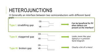


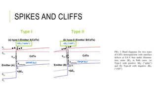


The document discusses lessons that can be learned from CdTe photovoltaics and applied to CZTS solar cells. Specifically, it examines how to engineer defect-tolerant heterojunction interfaces through three key factors: 1) the conduction band offset between materials, 2) emitter doping and thickness, and 3) the type of interface defects. Interface recombination can be reduced by creating a spike in the conduction band for type I heterojunctions or avoiding a cliff for type II heterojunctions. Defect-tolerant interfaces also depend on absorber inversion induced by emitter doping. However, comparisons between materials require consideration of interface mixing and surface reconstruction challenges.


![Human Reproduction [ Reproductive System ] Notes @irfanullah_mehar Irfanullah...](https://cdn.slidesharecdn.com/ss_thumbnails/humanreproductionreproductivesystemnotesirfanullahmeharirfanullahmeharjanantantra-260111172350-56e85778-thumbnail.jpg?width=640&height=640&fit=bounds)


